Wednesday, May 5, 2021

BASF and Umicore have entered a non-exclusive patent cross-license agreement for battery cathode active materials and their precursors

BASF and Umicore have entered into a non-exclusive patent cross-license agreement covering a broad range of cathode active materials (CAM) and their precursors (PCAM), including chemistries such as nickel cobalt manganese (NCM), nickel cobalt aluminum (NCA), nickel cobalt manganese aluminum (NCMA) and lithium rich, high manganese high energy NCM (HE NCM).

CAMs are critical for the performance, safety and cost of lithium-ion batteries used in modern electromobility and other applications. The interplay between PCAM and CAM and the development of these materials are crucial to maximize battery cell performance. For many years, BASF and Umicore have been investing intensively in product innovation for low, medium and high nickel PCAM and CAM resulting in each company owning sizeable and largely complementary patent portfolios.


BASF Research on high-performance battery materials at BASF’s laboratory in Ludwigshafen, Germany (above). Umicore 3D open battery cell (below).

Building on each other’s strong product technology expertise to support the technological needs of their customers, BASF and Umicore have entered into a landmark patent agreement allowing both partners to combine a wider range of IP-protected technologies related to features such as chemical composition, powder morphology and chemical stability. The agreement increases both parties’ ability to customize their materials to meet the increasingly diversified and complex customer requirements at the battery cell and application level. Furthermore, through this agreement both parties can increase even more their product development speed demonstrating their commitment to addressing the main challenges e-mobility is facing, such as energy density, safety and cost while enhancing transparency and reducing IP-risks for battery cell manufacturers and their customers.

The agreement covers more than 100 patent families filed in Europe, US, China, Korea and Japan. Both parties retain the right to enforce their own IP-rights against third parties in the future.

“This agreement with Umicore enables even faster, more sustainable and innovative battery materials development to serve our customers including battery cell manufacturers and automotive,” said Dr. Peter Schuhmacher, President of BASF Catalysts. “The continuous development of battery materials will accelerate the transformation towards full electrification and thus support the world’s efforts to fight climate change.”
Marc Grynberg, CEO of Umicore, commented: “This agreement with BASF is an important step in promoting cathode material innovation. It strengthens our technology positioning and further increases our ability to develop bespoke solutions which meet the most stringent performance and quality standards of our battery and automotive customers.”

Imec and AIXTRON Demonstrate 200 mm GaN Epitaxy on AIX G5+ C

Imec and AIXTRON Demonstrate 200 mm GaN Epitaxy on AIX G5+ C for 1200V Applications with Breakdown in Excess of 1800V

LEUVEN (Belgium), APRIL 29, 2021 — Imec, a world-leading research and innovation hub in nanoelectronics and digital technologies, and AIXTRON, the leading provider of deposition equipment for compound semiconductor materials, have demonstrated epitaxial growth of gallium-nitride (GaN) buffer layers qualified for 1200V applications on 200mm QST® substrates, with a hard breakdown exceeding 1800V. The manufacturability of 1200V-qualified buffer layers opens doors to highest voltage GaN-based power applications such as electric cars, previously only feasible with silicon-carbide (SiC)-based technology. The result comes after the successful qualification of AIXTRON’s G5+ C fully automated metal-organic chemical vapor deposition (MOCVD) reactor at imec, Belgium, for integrating the optimized material epi-stack.

AIX G5+ C reactor module with cassette-to-cassette wafer handler (www.aixtron.com)

Wide-bandgap materials gallium-nitride (GaN) and silicon-carbide (SiC) have proved their value as next-generation semiconductors for power-demanding applications where silicon (Si) falls short. SiC-based technology is the most mature, but it is also more expensive. Over the years tremendous progress has been made with GaN-based technology grown on for example 200mm Si wafers. At imec, qualified enhancement mode high-electron-mobility transistors (HEMTs) and Schottky diode power devices have been demonstrated for 100V, 200V and 650V operating voltage ranges, paving the way for high-volume manufacturing applications. However, achieving operating voltages higher than 650V has been challenged by the difficulty of growing thick-enough GaN buffer layers on 200mm wafers. Therefore, SiC so far remains the semiconductor of choice for 650-1200V applications – including for example electric cars and renewable energy.

For the first time, imec and AIXTRON have demonstrated epitaxial growth of GaN buffer layers qualified for 1200V applications on 200mm QST® (in SEMI standard thickness) substrates at 25°C and 150°C, with a hard breakdown exceeding 1800V. Denis Marcon, Senior Business Development Manager at imec: “GaN can now become the technology of choice for a whole range of operating voltages from 20V to 1200V. Being processable on larger wafers in high-throughput CMOS fabs, power technology based on GaN offers a significant cost advantage compared to the intrinsically expensive SiC-based technology.”

Key to achieving the high breakdown voltage is the careful engineering of the complex epitaxial material stack in combination with the use of 200mm QST® substrates, executed in scope of the IIAP program The CMOS-fab friendly QST® substrates from Qromis have a thermal expansion that closely matches the thermal expansion of the GaN/AlGaN epitaxial layers, paving the way for thicker buffer layers – and hence higher voltage operation.

Dr. Felix Grawert, CEO and President of AIXTRON “The successful development of imec’s 1200V GaN-on-QST® epi-technology into AIXTRON’s MOCVD reactor is a next step in our collaboration with imec. Earlier, after having installed AIXTRON G5+C at imec’s facilities, imec’s proprietary 200mm GaN-on-Si materials technology was qualified on our G5+ C high-volume manufacturing platform, targeting for example high-voltage power switching and RF applications and enabling our customer to achieve a rapid production ramp-up by pre-validated available epi-recipes. With this new achievement, we will be able to jointly tap into new markets.” Currently, lateral e-mode devices are being processed to prove device performance at 1200V, and efforts are ongoing to extend the technology towards even higher voltage applications. Next to this, imec is also exploring 8-inch GaN-on-QST® vertical GaN devices to further extend the voltage and current range of GaN-based technology.

EMD Electronics Creates Center of Excellence for Atomic Engineering by Combining Thin Films R&D Lab with Intermolecular

  • Unique capabilities with novel organo-metallic precursors and applications will enable customers to explore and test advanced materials for next-generation devices
  • Centralized innovation hub to speed up the delivery of material solutions to customers
San Jose, Calif., May 04, 2021 – EMD Electronics, a business of Merck KGaA, Darmstadt, Germany, today announced the creation of a Center of Excellence for atomic engineering at Intermolecular’s San Jose facility. The capabilities of EMD Electronic’s Thin-Films Applications R&D lab have been merged with Intermolecular’s advanced electronics capabilities to create a centralized innovation hub for our customers. This will enable seamless integration of testing and deposition of new materials for next-generation devices.


EMD Electronics "We've established a Center of Excellence for Atomic Engineering! Our  Thin Films Applications R&D lab has merged with Intermolecular's advanced electronics capabilities to create a centralized innovation hub for our customers. This will enable seamless integration of testing and deposition of new materials for next-generation semiconductors." (Quote and photo above from EMD Electronics LinkedIn Announcement LINK)

“Intermolecular’s 150,000 sqft facility in the heart of Silicon Valley is the perfect center to converge materials innovation and testing for our global customers,” said Anand Nambiar, Head of Semiconductor Materials business unit at EMD Electronics. “To continue scaling down to advance nodes and develop next-generation applications, a reliable supply of innovative materials is required. Our expertise in atomic engineering in combination with Intermolecular’s unique tools and processes, will enable our customers to test, validate, prototype and introduce new advanced technologies and materials faster in the market.”

“Ongoing miniaturization drives our customers to build their devices from the atoms up in complex 3D arrangements. Our advanced deposition materials allow them to create differentiation in their products,” said Casper van Oosten, Business Field Head and Managing Director for Intermolecular, Inc. “Until now, the value chain process to test and validate materials involved multiple steps and was time consuming. By combining capabilities, we now have access to the right team, tools and data and can provide our customers with a more seamless integration to prove new organometallic materials for electronic applications.”

On March 4, Merck KGaA, Darmstadt, Germany moved the Silicon Valley Innovation Hub to San Jose’s Intermolecular site creating a unique space for innovation and collaboration with start-ups at the intersection of life science, healthcare and electronic materials. The building boasts 30,000 square feet of cleanroom, chemical labs, offices, a collaboration area and event spaces. Intermolecular, Inc. (“Intermolecular”) is the trusted partner for materials innovation and a wholly-owned subsidiary of the EMD Electronics business of Merck KGaA, Darmstadt, Germany.

About EMD Electronics

EMD Electronics is the North America electronics business of Merck KGaA, Darmstadt, Germany. EMD Electronics’ portfolio covers a broad range of products and solutions, including high-tech materials and solutions for the semiconductor industry as well as liquid crystals and OLED materials for displays and effect pigments for coatings and cosmetics. Today, EMD Electronics has approximately 2,000 employees around the country with regional offices in Tempe (AZ) and Philadelphia (PA). For more information, please visit www.emd-electronics.com.

About Intermolecular

Intermolecular is a trusted partner for materials innovation and the Silicon Valley science hub of Merck KGaA, Darmstadt, Germany and its electronics business. Intermolecular explores, tests and develops advanced materials that are revolutionizing the next generation of electronics that make lives easier, entertaining and more productive. For more than 15 years, the team, methodologies and quality data have driven impactful outcomes, market opportunities and innovative product designs for customers.

About Merck KGaA, Darmstadt, Germany

Merck KGaA, Darmstadt, Germany, a leading science and technology company, operates across healthcare, life science and electronics. Around 58,000 employees work to make a positive difference to millions of people’s lives every day by creating more joyful and sustainable ways to live. From advancing gene editing technologies and discovering unique ways to treat the most challenging diseases to enabling the intelligence of devices – the company is everywhere. In 2020, Merck KGaA, Darmstadt, Germany, generated sales of € 17.5 billion in 66 countries.

The company holds the global rights to the name and trademark “Merck” internationally. The only exceptions are the United States and Canada, where the business sectors of Merck KGaA, Darmstadt, Germany operate as EMD Serono in healthcare, MilliporeSigma in life science, and EMD Electronics. Since its founding 1668, scientific exploration and responsible entrepreneurship have been key to the company’s technological and scientific advances. To this day, the founding family remains the majority owner of the publicly listed company.

Tuesday, May 4, 2021

CBS 60 Minutes - Chip shortage highlights U.S. dependence on fragile supply chain

Seventy-five percent of semiconductors, or microchips — the tiny operating brains in just about every modern device — are manufactured in Asia. Lesley Stahl talks with leading-edge chip manufacturers, TSMC and Intel, about the global chip shortage and the future of the industry.
  • Pat Gelsinger: 25 years ago, the United States produced 37% of the world's semiconductor manufacturing in the U.S. Today, that number has declined to just 12%
  • Within the world of global collaboration, there's intense competition. Days after Intel announced spending $20 billion on two new fabs, TSMC announced it would spend $100 billion over three years on R&D, upgrades, and a new fab in Phoenix, Arizona, Intel's backyard, where the Taiwanese company will produce the chips Apple needs but the Americans can't make.

Intel CEO Pat Gelsinger shows CBS correspondent Lesley Stahl a silicon wafer.

Monday, May 3, 2021

APTC from South Korea is developing CVD, ALD and oxide etcher systems as it expands its portfolio

Since 2002, APTC has engaged in the manufacturing of dry etcher systems for mass semiconductor production. Today, the company supplies 300mm plasma etching systems, 200mm plasma etching systems, plasma doping systems, and light-emitting-diode etching systems. Over the past 19 years, APTC has been an established supplier for SK Hynix in South Korea and its mass production subsidiaries in China. SK Hynix is the second-largest memory chipmaker and third-largest semiconductor company globally.

300 mm Leo Poly Etcher system from APTC

With its numerous patents, awards, original plasma source technology and market leadership as South Korea’s sole domestic supplier of poly etching equipment, APTC is gearing up for growth at home and overseas. Fully committed to research and development (R&D) in pursuit of quality and innovation, APTC has invested US$20 million in American engineering capabilities, maintaining an R&D office in the United States, where it aims to work with tier-one semiconductor companies.

Listed on the Korea Exchange under the leadership of its current CEO, the company has revitalized its business strategy with plans to explore new markets, new clients, and new technologies. The state-of-the-art plasma technology also has a number of applications in the next-generation dry etch sector and its related innovations.

In semiconductor manufacturing, chemical vapor deposition (CVD) is a method used to produce high-performance and high-quality solid materials such as thin film in a vacuum, while atomic layer deposition (ALD) is a vapor phase technique of laying thin films on a substrate. APTC is developing CVD, ALD, and oxide etcher systems as it expands its portfolio of offerings.

Source: New strategy, markets and innovation fuel APTC’s rise in semiconductor etcher systems (LINK)

Saturday, May 1, 2021

Jusung to spend 36.3 billion won to build new production facility

Fab ALD and CVD equipment firm Jusung Engineering will spend 36.3 billion won to build a new production facility in Gwangju, where the company is based, it said on Thursday. In addition, it is reported that Jusung recently sold SK Hynix 30 ALD systems.

Source: Jusung to spend 36.3 billion won to build new production facility


Nanexa AB started the first clinical study with ALD based PharmaShell® at the Karolinska University Hospital

Nanexa AB (publ) today announces that the company has started its first clinical study with PharmaShell®, a phase I study in Nanexa's product project NEX-18, at the Karolinska University Hospital.


The study aims to show that the company's NEX-18 product, a long-acting formulation of azacitidine (the active substance in the drug Vidaza), provides the desired safety and pharmacokinetic profile. In the study, two doses of NEX-18 will be studied. The study will be conducted at Karolinska University Hospital in Stockholm and Akademiska Sjukhuset in Uppsala.

“The start of this study is a very big milestone in Nanexa's development. It is with great enthusiasm that we now see that the study is getting started. We expect the study to be completed during the third quarter.”, said David Westberg, CEO of Nanexa.

The NEX-18 product is being developed to improve the treatment of MDS (Myelodysplastic Syndrome), a form of hematological cancer that mainly affects the elderly. This is done by utilizing the unique properties of the PharmaShell® concept to create a controlled release depot formulation. Today's treatment means that injections are given at hospitals seven days in a row each month. The goal of the NEX-18 project is to simplify treatment by only having to give one injection. In addition to greatly simplifying for patients, Nanexa sees that NEX-18 will provide significant cost savings compared to current treatment.

“With the results of this study, we intend to continue the clinical development with a phase II study to achieve clinical Proof of Concept. After that, the goal is to run NEX-18 further towards commercialization, either through a license partner or as an own project, whatever option is deemed to create most value for Nanexa”, said David Westberg.

ALD – The coating technology behind the drug delivery system PharmaShell®

The technology used by Nanexa to manufacture the shells that make up PharmaShell® is Atomic Layer Deposition (ALD). In ALD, reactive gases are used which, with atomic layer by atomic layer, build up a surface coating with high precision. ALD has been used in the electronics industry for decades and is thus well established for larger scale production and automation.

ALD can also be used at low temperatures, down to room temperature, unlike other surface coating techniques which usually use considerably higher deposition temperatures, thereby risking inactivating the drug. A further advantage of ALD is that the coating is carried out under dry conditions, which makes it possible to coat drugs that are quickly dissolved in water or other solvents.

By building up an atomic layer for atomic layer with ALD, the thickness of the coating can be controlled with extremely high precision. Drug particles of various sizes and shapes can be coated since the only thing required for coating to be formed is that the reaction gases can reach the surface.
About Nanexa AB (publ)

Nanexa AB is a nanotechnology drug delivery company focusing on the development of PharmaShell®, a new and groundbreaking drug delivery system with great potential in a number of medical indications. Within the framework of PharmaShell®, Nanexa has partnership agreements with among others, AstraZeneca.

Friday, April 30, 2021

The US Patent Office has approved AlixLabs’ patent application for nanofabrication by ALE Pitch Splitting (APS)

(30 April 2021, Lund Sweden). The US Patent Office has approved AlixLabs’ (AlixLabs AB) patent application for nanofabrication by ALE Pitch Splitting (APS).

The US Patent Office has issued a patent (US10930515) on February 23, 2021. The patent covers methods to split nanostructures in half by a single process step using Atomic Layer Etching (ALE). The method has the potential to have a big impact on the semiconductor industry by enabling sustainable scaling of electronic components and shrink chip designs further in a cost-effective way. The method is complementary for single exposure Immersion and Extreme UV (EUV) Lithography and corresponding multiple patterning technologies like self-aligned double and quadruple patterning (SADP resp. SAQP) as well as directed self-assembly (DSA).

In direct comparison to mentioned more complicated and expensive methods, APS may cut the need for certain fab equipment investments considerably, reduce manufacturing cost and energy consumption as well as reduce greenhouse gas emission during the patterning processing by up to 50%, allowing greener and affordable way forward for the semiconductor industry.

AlixLabs aims at applications for the manufacturing of leading-edge sub 5nm Logic Devices and Memory Chips that are used for everyday consumer electronic devices, 5G and AI.

The company’s CEO Dr. Jonas Sundqvist comments:

After founding the company in 2019 we now move into very exciting times. The team has been expanded with Dr. Mohammad Karimi as Principal Scientist and we have several applications and projects in the pipeline for broadening our patent protection and creating further opportunities for commercial agreements starting now. Currently, we are taking on the first round of private investments and will expand operations for both core activities in Lund, Sweden, at NanoLund and Lund Nano Lab, and the IDEON Science Park in Sweden. In addition, we are heading to the heart of the European semiconductor industry in Dresden Germany for a lab to fab transfer to 300 mm silicon wafer process verification to get ready for customer demonstrations of APS.

The company’s CTO Dr. Dmitry Suyatin comments:

This patent is built on a surprising discovery by the inventors, which took place at Lund Nano Lab during the Master project by Dr. Sabbir A. Khan who has recently received his PhD from the University of Copenhagen and now continues his postdoctoral work at Niels Bohr Institute in Copenhagen.

About AlixLabs AB:

AlixLabs (www.alixlabs.com) is an innovative startup enabling the semiconductor industry to scale down Logic and Memory components in a cost-effective manner by the use of ALE Pitch Splitting (APS).

Background Information:


Picture:


Thursday, April 29, 2021

Frontiers in Materials Manufacturing: Materials for Printed Hybrid Electronics

The U.S. Department of Energy’s Argonne National Laboratory scientists are hosting a webinar on May 19 that will explore the challenges and opportunities for materials in printable hybrid electronics.


These devices will transform how we view and use electronics in our daily life. Wearable health devices, sensors, and antennas will be cheaper, more versatile, and draw less power. But challenges remain, especially when creating and designing the right materials.

Angel Yanguas-Gil, Principal Materials Scientist, Argonne National Laboratory will talk about how the combination of novel materials (with and without ALD) and brain-inspired computing can enable smart sensors and edge computing based on printed electronics.

During this webinar, scientists and experts from IDTechEx, NextFlex and other organizations will describe the state-of-the-art for materials in this area. Experts will also explain the scientific advances that will lead to the next generation of printed electronics.

Hear from experts including:
  • Matthew Dyson, Technology Analyst, IDTechEx
  • Eric Forsythe, Program Manager, NextFlex Manufacturing Institute, Army Research Laboratory
  • Stijn Gillissen, Global Head Printed Electronics, Henkel
  • Mark Hersam, Walter P. Murphy Professor of Materials Science and Engineering, Northwestern University
  • Melbs LeMieux, Co-Founder and President, Electroninks
  • Matthew Tirrell, Dean of the Pritzker School of Molecular Engineering and Robert A. Millikan Distinguished Service Professor, University of Chicago; Senior Scientist, Argonne National Laboratory
  • Sihong Wang, Assistant Professor of Molecular Engineering, University of Chicago
  • Angel Yanguas-Gil, Principal Materials Scientist, Argonne National Laboratory


Kenneth Hörhammer joins Picosun as Vice President, Sales

ESPOO, Finland, 29th of April 2021 – Picosun Group has appointed Kenneth Hörhammer as Vice President, Sales, and a member of Picosun Group’s Leadership Team as of May 1, 2021.


"The potential for ALD is almost limitless, and Picosun is spearheading this technology globally." 


Kenneth Hörhammer has strong international business experience as well as passion and proven results in sales development and execution. Before joining Picosun, Kenneth Hörhammer has held multiple global business and sales leadership positions at Vaisala both in Finland and abroad in the past 17 years.

“I am excited to join this fantastic team and company. The potential for ALD is almost limitless, and Picosun is spearheading this technology globally. Picosun is a bright example of Finnish high-tech innovativeness, and I am thrilled to become an integral part of this international growth story,” states Kenneth Hörhammer.

“I warmly welcome Kenneth Hörhammer to join our team. The professional background and global experience he brings to our team enable us to significantly strengthen our global sales management, build a stronger sales organization and enforce customer satisfaction,” concludes Jussi Rautee, CEO of Picosun Group.

Friday, April 23, 2021

Beneq and E+R Group enter strategic partnership for roll-to-roll ALD

The revolutionary Genesis ALD platform enables next-generation battery manufacturers to scale up quickly

Beneq, a leading ALD equipment manufacturer, today announces a strategic partnership with E+R to design and commercialize innovative roll-to-roll ALD systems for R&D and volume production. The companies have together developed a revolutionary roll-to-roll ALD system.


The new ALD platform – named Genesis ALD – is targeted at various industrial R2R ALD applications, including:
  • Passivation of cathodes and anodes for various types of lithium-ion and solid-state batteries
  • Conductive layers and encapsulation for flexible solar cells
  • Moisture barriers for flexible electronics
“Bringing Beneq’s unique roll-to-roll ALD technology together with Emerson & Renwick’s deep experience in roll-to-roll vacuum and web handling is good news for the battery industry,” says Sami Sneck, Business Executive at Beneq.

“The partnership allows us to offer state-of-the-art atomic layer deposition technology for enhancing li-ion and other next-generation batteries, where we expect to see strong market demand. There is a lot of potential for this technology in other application areas too, but the market for those end-products is yet to mature,” says Sneck.

“We have worked very well with Beneq and both companies have a good grasp of the potential markets available,” says Andrew Jack, Sales Director at E+R Group. “ E+R offers a wide range of high-end R2R vacuum equipment. This collaboration makes it easier to integrate R2R ALD with other techniques where necessary.”

The partnership is effective immediately. For inquiries, visit www.beneq.com/en/contact-us.

Genesis ALD

World’s only commercially available roll-to-roll ALD system. Learn more.


Thursday, April 22, 2021

Highlights of Prof. Erwin Kessels’ Recent Webinar on “Plasma-Assisted Atomic Layer Deposition: From Basics to Applications” Organized by the American Vacuum Society (AVS)

On the 10th of February, 2021, Prof. Erwin Kessels from Eindhoven University of Technology, Netherlands, delivered a 4-hour long webinar, full of highly valuable content, on Plasma-Assisted (Enhanced) Atomic Layer Deposition (PAALD/PEALD). For those who missed this wonderful opportunity to have an insight into one of the most advanced deposition processes in the semiconductor chip production line today, Abhishekkumar Thakur, Associated Technology Analyst with BALD Engineering AB has come up with some interesting highlights and key takeaways from Prof. Kessels' webinar from when we took part:


February 10, Erwin Kessels will present an AVS Webinar: Plasma-Assisted Atomic Layer Deposition: From Basics to Applications. Learn more at https://avs.swoogo.com/webinar_pald

Interesting Highlights and Key Takeaways

1. The current deposition wafer fab equipment market size for ALD has grown as big as or even bigger than that for PVD (Physical Vapor Deposition), but still less than that for CVD (Chemical Vapor Deposition)

2. Semiconductor processing plasmas exist under non-equilibrium conditions, i.e., the electrons present in the plasma are heated by the applied electric field up to a temperature of 50,000 K (~5eV) as opposed to the relatively low gas temperature (300-500 K) due to the low pressures. This is the reason that PEALD becomes useful in the deposition of the high-quality thin-films on thermally fragile substrates/structures, e.g., plastic, foil, photoresist, etc.

3. Electron Energy Distribution Function (EEDF) together with the electron impact cross-section with the events occurring in the plasma (e.g. dissociation, excitation, ionization, etc.) determines the density of a particular species in the plasma (e.g. ions, radicals, etc.)

Ref: https://doi.org/10.1116/6.0000145

4. The thickness of the plasma sheath is typical ~0.1 to 10mm depending on the electron density, the electron temperature, and the potential difference between the plasma and the surface in contact with the plasma (the larger the potential difference is, the thicker the sheath is). The plasma sheath bends along the surface of the macroscopic objects and ions strike every surface of the object orthogonally. However, the plasma sheath can’t follow the surface of the microscopic features (e.g. microscopic trenches in a wafer), thus the ions bombard only the top and the bottom flat surfaces of the features.

5. Plasma source can also be a big source of Oxygen contamination when gets eroded by ion bombardment. It’s especially a big problem in the PEALD of nitrides in ICP systems. In this regard, the use of Alumina as a dielectric window in an ICP system can lead to less sputter yield than that from the use of Quartz as a dielectric window, thereby providing better quality nitride films. This is the reason why many companies have adopted Hollow Cathode Plasma source developed by Meaglow Ltd. in their systems.

6. Vacuum systems themselves can also be a source of Oxygen contamination, especially the ALD reactors because they typically don’t have very low base pressure; usually ~10-6 Torr after utilizing a turbo molecular pump. If the ALD cycle times are relatively long such that the reactive surfaces are exposed to the (“poor”) vacuum for a relatively long time, the Oxygen concentration in the deposited film increases. In other words, the faster the ALD process is, the less contaminated the deposited film is.


An example was given from ALD of HfN from Research of Saurabh Karwal from TU Eindhoven (To be published in 2021) studying the impact of oxygen incorporation by artificially extended cycle times.


7. Strong pumping does not only lead to a better vacuum and in turn less Oxygen contamination in the deposited film, but it also helps reduce the gas residence time inside the reactor minimizing the surface reaction by-products being cracked in the plasma and redepositing on the surface. Thus, a higher pumping speed results in a higher quality film growth.

8. Regarding the conformal growth of an ALD film: When S0*AR2 < 0.1, the film growth is reaction-limited, and extending the precursor/co-reactant dose (beyond the saturation dose) will not make any difference in the film conformality. It’s similar to the growth on a planar substrate. However, when S0*AR2 > 100, the film growth is diffusion-limited, and hence, the precursor/co-reactant dose, that needs to be applied to get a fully conformal growth in the trench, scales with the AR2. In the case of PEALD, the film growth can be recombination limited too, and it becomes even difficult to get a conformal film growth because of the co-reactant dose that needs to be applied to get a fully conformal growth in the trench scales exponentially with the AR. The conformality becomes further difficult to achieve when the surface recombination probability r of the radicals strengthens. Moreover, the conformality of the PEALD film depends heavily on the film material to be deposited because the surface recombination probability of the radicals heavily depends on the material, e.g., SiO2 films can go much deeper into the trench than Al2O3 or HfO2 films since the surface recombination probability of O radicals on SiO2 is much lower than that on Al2O3 or HfO2. The surface recombination probability also depends on the substrate temperature and the process pressure.

[S0 = Sticking probability with zero surface coverage, AR = Aspect Ratio of the trench]

9. PEALD film properties are strongly dependent on ion-energy dose = plasma exposure time*ion flux*mean ion energy. By applying substrate biasing, i.e., by employing mild ion bombardment, mass density, refractive index, crystalline properties, resistivity, void fraction, residual stress, surface roughness, thickness uniformity, chemical composition, topographic selectivity, etc. of the deposited film can be tuned.

10. Plasma can cause radiation damage in the PEALD films because plasma also comprises radiation in the vacuum ultraviolet (VUV) region (i.e. wavelengths below 200nm) generating VUV photons that can have energy up to even 10-40 eV. However, this certainly can’t disqualify plasma processing in the semiconductor industry because there are methods to avoid the adverse impact of VUV photons, e.g., working at higher process pressure as the VUV photons are easily absorbed by the gas.

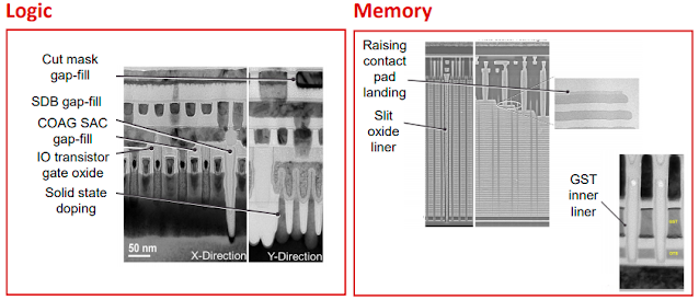
11. Some of the applications of PEALD in the Logic HVM include cut mask gap-fill, single diffusion break (SDB) gap-fill, contact over active gate (COAG) self-aligned contact (SAC) gap-fill, gate oxide for the IO transistors, solid-state doping, patterning hard-mask, etc. and in the Memory HVM include raising contact pad landing by depositing SiN, slide oxide line, GST X-point (phase-change) memory inner liner, etc. Topographically selective PEALD has been in use in 3D NAND production. The biggest PEALD market at present is that of self-aligned multiple patterning with SiO2 since 22 nm node. It’s important here to note that more than 50% of the PEALD layers are sacrificial and don’t show up in the device! PEALD of SiO2 has also been in the display market, e.g., in a barrier stack against moisture permeation in the curved plastic OLED displays in the Cadillac Escalade 2021. In addition to that, PEALD SiO2 has also found its application in the nanoscale encapsulation of perovskite nanocrystal luminescent films to enhance its stability against water, light, and heat.

Wednesday, April 21, 2021

ASM International and ALD opens up 2021 with a strong quarter in Logic & Foundry segment

ASM International N.V. (Euronext Amsterdam: ASM) today reports its first quarter 2021 operating results (unaudited) in accordance with IFRS.

  • New orders at €411 million were 8% above the level of last quarter.
  • Revenue for the first quarter of 2021 was €394 million and increased 14% compared to the previous quarter due to strong market demand.
  • The gross profit margin was 49.5% in Q1 2021 compared to 45.2% in the previous quarter, mainly due to a favorable mix.
  • The operating result was €125 million compared to €78 million in the previous quarter.
  • Normalized net earnings for the first quarter of 2021 were €125 million, €43 million higher compared to Q4 2020.
LINKS
Q12021 Presentation: LINK
Earings Call Transcript (Seeking Alpha): LINK
  • Gartner expects WFE to increase by 23% in 2021 (April 2021), up from +8% still predicted in December 2020
  • VLSI Research expects WFE to increase by 22% in 2021 (April ’21), up from a previous forecast of +12% last February

“2021 started very strong for ASM,” said Benjamin Loh, President and Chief Executive Officer of ASM International. “In the first quarter, we realized revenue of €394 million, well within our guidance of €380-400 million and up 14% from the level in Q4. The revenue level was again driven by continuous high demand in the logic/foundry segment. Our Q1 order intake, at €411 million, was up 8% from an already high level in Q4 and ahead of our guidance of €380-400 million, driven by solid demand in logic/foundry. Our gross margin was at a high level of 49.5%, caused by a favorable mix, while our operational cash flow showed a record high level in Q1. Based upon the strong cash position at the end of March, we plan to start a new €100 million share buyback program.”

Outlook

For Q2, on a currency comparable level, we expect revenue of €390-€410 million. Q2 bookings, on a currency comparable level, are expected to be in the range of €420-€440 million.

“Based upon the current market developments, the wafer fab equipment (WFE) market is expected to grow by a high-teens to low twenties percentage in 2021.”

Based upon the current market developments, the wafer fab equipment (WFE) market is expected to grow by a high-teens to low twenties percentage in 2021. 2021 is expected to develop in another year of solid growth for ASM. Based upon our current view, we expect our sales in the second half to be at least at the same level as in the first half.

ALD and New Market segment

"Moving to the longer-term outlook, ALD continues to be an important, long-term growth market for ASM. For 2020, we estimate the single wafer ALD market, to reach the size of US$1.5 billion in line with the expectations we put out several years ago. We are currently reviewing our focus and expect to present the new market for customers later in the year. However, it is clear to us that ALD will remain the fastest-growing segment of the deposition market, with substantial, double-digit growth potential in the coming years. ALD is a critical technology for our industry to develop the next generation's faster processes and memory devices that in turn will enable the growth of key markets such as in 5G and artificial intelligence." - Benjamin Loh

DRAM and High-k/Metal Gate adaption with ALD

ASM's recent most significant achievement in expanding our memory presence has been in ALD wins for high-k metal gate in the high-performance DRAM segment, with the leading memory players. It is a key technology that reduces device leakage and thereby supports increases in both energy efficiency and device performance. As reported earlier, ASM books their first meaningful sales for this application last year and expects it to support a healthy increase in our DRAM sales this year.

What has been launched today is primarily what is called the high-performance DRAM segment or sub-segment within the DRAM market and it has been adopted by all the DRAM manufacturers.

ASM ALD Market Share

According to the information given in the call, Gartner report ASM´s market share in the single wafer ALD market has grown from 57% to 60% during 2020 and Benjamin Loh agreed that that estimate is in the right direction. 


Tuesday, April 20, 2021

Spatial atomic layer depos­ition system FHR.Star.400x300-SALD delivered

FHR (Press Release) has suc­cess­fully delivered the FHR.Star.400x300-SALD. This is FHR’s first machine using spa­tial atomic layer depos­ition (spa­tial ALD). The sys­tem is cap­able of depos­it­ing films on both 200 mm wafers and tex­tiles or other 3D sub­strates of up to 400 x 300 x 10 mm³.


Spa­tial ALD allows for high speed and highly con­formal coat­ings on flat as well as micro-struc­tured sur­faces. Applic­a­tions are dielec­tric lay­ers for anti-reflect­ive coat­ings on lenses as well as coat­ings for elec­trical insu­la­tion or pro­tec­tion against mois­ture or oxy­gen applied to energy sys­tems, med­ical devices or func­tion­al­ized tex­tiles.


In its base con­fig­ur­a­tion, the FHR.Star.400x300-SALD is made for thermal ALD on up to eight wafers or four 3D sub­strates in par­al­lel. For Al2O3 on wafers, depos­ition rates of 5-10 nm/​min and thick­ness non-uni­form­it­ies <± 2.0% have been reached. A large blind flange allows to add other thin film tech­no­lo­gies or plasma treat­ment and the machine is already pre­pared to for in-situ ellip­so­metry and trans­mis­sion spec­tro­scopy for improved pro­cess con­trol. To fur­ther increase the pro­ductiv­ity, the FHR.Star.400x300-SALD can be included in a cluster setup with a cent­ral hand­ling robot cham­ber, load locks, pre-treat­ment cham­bers or other pro­cess cham­bers.


FHR, Marian Böh­ling (CSO): „ALD coat­ing tech­no­logy is val­ued for its unique con­form­al­ity and pre­ci­sion even on 3D sub­strates but claimed to be slow and there­fore often ignored. Our FHR.Star.400x300-SALD refutes this claim impress­ively and makes ALD avail­able as an excit­ing and prom­ising thin film tech­no­logy for a wide range of indus­trial applic­a­tions. Installed at a world-class thin film research insti­tute, this FHR.Star.400x300-SALD offers a low-threshold access for every­body inter­ested in using ALD for own products.“

FHR Anla­gen­bau GmbH - The Thin Film Com­pany was foun­ded in 1991 and offers tailor-made vacuum coat­ing sys­tems and sput­ter­ing tar­gets as well as coat­ing and equip­ment ser­vice from a single source.

The close cooper­a­tion with our cus­tom­ers starts with the pro­cess devel­op­ment and con­tin­ues with the devel­op­ment of pilot scale up to mass pro­duc­tion. Our port­fo­lio integ­rates the tech­no­lo­gies sput­ter­ing, evap­or­a­tion, PECVD and ALD into the equip­ment types cluster, inline, roll-to-roll and batch. Based in Ger­many and with sys­tems installed world­wide in vari­ous indus­tries such as semi­con­duct­ors, MEMS, elec­tron­ics, sensor tech­no­logy, optics, photo­vol­ta­ics, etc., we will jointly find vacuum coat­ing solu­tion for our cus­tom­ers.

Con­tact
FHR Anla­gen­bau GmbH
Mar­ket­ing & Com­mu­nic­a­tion
Phone: +49 35205 520-0
E-mail: mar­ket­ing@fhr.de

Saturday, April 17, 2021

Unraveling the different causes behind ferroelectricity in HfO2

Interplay between oxygen defects and dopants: effect on structure and performance of HfO2-based ferroelectrics

Monica Materano et al
Inorg. Chem. Front., 2021, Advance Article https://doi.org/10.1039/D1QI00167A

Abstract: Ten years after the first report on ferroelectricity in HfO2, researchers are still occupied unraveling the different causes behind this phenomenon. Among them, oxygen related defects seem to play a major role, affecting both crystalline phase formation and performance of HfO2-based devices. This review surveys the available literature and provides a broad picture on the topic, starting with an overview of existing oxygen-related defects, assessing the extensive calculations and experimental reports on phase stabilization in both undoped and doped HfO2 and concluding with a discussion of device reliability involving oxygen vacancies, first in more classical HfO2 applications such as MOSFET high-k metal gate and resistive switching devices and later in the three major groups of ferroelectric non-volatile memory devices.


Friday, April 16, 2021

ALD coating for delayed drug delivery via the lungs for the treatment of respiratory diseases by Astra Zeneca and TU Delft

The medical thin film coating segment is a mature and growing market for CVD & PVD coating equipment and ALD is an emerging segment. Applications are :
  • electronic implants (IC, BioMEMS, Pacemaker) 
  • prosthetic implants (spine, trauma, hip, knee, dental)
  • active pharmaceuticals ingredients for  delayed drug delivery

ALD has slowly but steadily moved into the field of medical and pharmaceuticals. Just as some examples Nanxa AB in Sweden and Applied Materials has a joint venture and Picosun in Finland and Veeco has very active business unit and offer ALD systems specifically for medical applications for several years. As well as several reports on applications such as dental, tissue engineering, smart lenses, and various electronic or prosthetic implants.

Here is a new application explored by Dutch TU Delft and British-Swedish Astra Zeneca using ALD coating for delayed drug delivery via the lungs for the treatment of respiratory diseases.

Controlled Pulmonary Delivery of Carrier-Free Budesonide Dry Powder by Atomic Layer Deposition
ACS Nano 2021, XXXX, XXX, XXX-XXX
Publication Date:March 26, 2021, https://doi.org/10.1021/acsnano.0c10040


Ideal controlled pulmonary drug delivery systems provide sustained release by retarding lung clearance mechanisms and efficient lung deposition to maintain therapeutic concentrations over prolonged time. Here, we use atomic layer deposition (ALD) to simultaneously tailor the release and aerosolization properties of inhaled drug particles without the need for lactose carrier. In particular, we deposit uniform nanoscale oxide ceramic films, such as Al2O3, TiO2, and SiO2, on micronized budesonide particles, a common active pharmaceutical ingredient for the treatment of respiratory diseases. In vitro dissolution and ex vivo isolated perfused rat lung tests demonstrate dramatically slowed release with increasing nanofilm thickness, regardless of the nature of the material. Ex situ transmission electron microscopy at various stages during dissolution unravels mostly intact nanofilms, suggesting that the release mechanism mainly involves the transport of dissolution media through the ALD films. Furthermore, in vitro aerosolization testing by fast screening impactor shows a ∼2-fold increase in fine particle fraction (FPF) for each ALD-coated budesonide formulation after 10 ALD process cycles, also applying very low patient inspiratory pressures. The higher FPFs after the ALD process are attributed to the reduction in the interparticle force arising from the ceramic surfaces, as evidenced by atomic force microscopy measurements. Finally, cell viability, cytokine release, and tissue morphology analyses verify a safe and efficacious use of ALD-coated budesonide particles at the cellular level. Therefore, surface nanoengineering by ALD is highly promising in providing the next generation of inhaled formulations with tailored characteristics of drug release and lung deposition, thereby enhancing controlled pulmonary delivery opportunities.

Thursday, April 15, 2021

BENEQ P800 coating batches of 300 mm showerhead plates for advanced semiconductor wafer processing equipment

How it is done - Here a cool video of a BENEQ P800 coating 300 mm showerhead plates for some advanced semiconductor wafer processing equipment.


Wednesday, April 14, 2021

Kurt J Lesker installs an ALD150LE system at the University of Minnesota Nano Centre

Kurt J. Lesker Company installs an ALD150LE system at the University of Minnesota Nano Centre. a state-of-the-art facility for interdisciplinary research in nanoscience and applied nanotechnology. The team there will be using the system for the deposition of a range of different films such as alumina (Al2O3), hafnium oxide (HfO2), titanium dioxide (TiO2), and zirconium dioxide (ZrO2). Read more about the facility here: https://www.mnc.umn.edu/


The Kurt J Lesker ALD test engineer, Tom Yurechko, snapped this great pic of the recent installation of our ALD 150LE at the University of Minnesota Nano Centre.


Characterization of Annealing and Dopant Activation Processes Using Differential Hall Effect Metrology (DHEM) by Active Layer Parametrics (ALP) Inc.

ALP’s Differential Hall Effect Metrology (DHEM) technique is the only technique that directly measures active dopant concentration, mobility, and resistivity depth profiles through semiconductor layers at sub-nm depth resolution (www.alpinc.net).


Above, cross-sectional TEM images of the P ion-implanted samples after annealing and corresponding depth profiles from DHEM.

ALP´s latest work employing this innovative technology and ALPro(TM) electrical profiling tools are summarized in a new invited paper titled “Characterization of Annealing and Dopant Activation Processes Using Differential Hall Effect Metrology (DHEM)”, which will be presented at the 239th ECS Meeting (May 30 to June 3 2021).

They showcase data developed jointly with Imec, Belgium, and Taiwan Semiconductor Research Institute (TSRI, Hsinchu) in the paper. You can read the abstract at (https://ecs.confex.com/ecs/239/meetingapp.cgi/Paper/147952). If you are interested in reading the full paper, please contact Dr. Joshi below for a preprint.

Abhijeet 'AJ' Joshi, PhD
CTO/Co-Founder
Active Layer Parametrics (ALP) Inc.
info@alpinc.net

Tuesday, April 13, 2021

Picosun increases efficiency for LED and OLED production

ESPOO, Finland, 13th of April 2021 – Picosun Group has proved to significantly increase the production efficiency of its LED and OLED customers with the PICOSUN® P-300BV ALD system. Recent tests show that a reduced ALD process cycle time and an increased number of wafers deposited with the same film thickness resulted in almost 100% better throughput. A throughput of over 20 000 wafers per month can be reached with a wafer batch of 100 wafers*. At the same time, the process quality in terms of film thickness uniformity has remained on an excellent level (<1% 1sigma) when measured within wafer, wafer to wafer as well as batch to batch.


“Picosun ALD solutions have become the standard in high volume ALD manufacturing. PICOSUN® P-300BV ALD system is designed especially for production of LEDs and OLEDs. With our experience and deep know-how in ALD we are continuously striving to minimize the total cost of ownership and ensure future-proofness for our customers”, states Juhana Kostamo, Vice President, Industrial Business Area of Picosun Group.

Global LED and OLED manufacturers trust in ALD in their production to achieve better device performance and longer product lifetimes. This is a result of thin, conformal, uniform and pinhole-free material layers deposited by ALD for passivation and moisture protection as well as for creating buffer and interface layers.

* 4” 100 wafers, >20000 WPM, <1% 1sigma WiW, <1% 1sigma WtW, <1% 1sigma BtB (120 nm TMA + H2O @ 200 oC)

Read more about PICOSUN® P-300BV at picosun.com/product/p-300bv/

Monday, April 12, 2021

Announcing ALD Russia 2021 Saint Petersburg, Russia 27–30 September 2021.

The 3rd International Workshop ‘Atomic Layer Deposition Russia 2021’ (ALD Russia 2021) will be held in Saint Petersburg, Russia 27–30 September 2021.

Conference Web: http://technolog.edu.ru/aldrussia/general-information-en.html


The 3rd International Workshop ‘Atomic Layer Deposition Russia 2021’ (ALD Russia 2021) will be held at the Saint-Petersburg State Institute of Technology from 27 to 30 September 2021. That will be the 3rd such event in the series that started in Moscow in 2015 and continued in Saint Petersburg in 2017.

The workshop will mark the 90th anniversary of the birth of Stanislav Ivanovich Koltsov (1931–2003), whose pioneering studies in 1960s laid the foundation of molecular layering, the method of synthesis of surface compounds and thin films widely known today as atomic layer deposition (ALD).

All scholars interested in ALD are welcome to attend the event and submit their latest results on any aspect of ALD, including its chemical foundations, new materials and processes, industrial applications and instrumentation.

The topic of the workshop is the current state of research in the field of atomic layer deposition and commercialisation of its results.


Saint Petersburg State Institute of Technology (Technical University)

Spatial Atomic Layer Deposition (SALD): Essential for today's and future battery production

SALD is a carve-out of the brainport Eindhoven-based OEM company SoLayTec, which develops and sells advanced spatial ALD machines specifically for mass-produced solar cells. Because there were a lot of requests for applications other than solar cells, the company SALD was founded in 2019. In the relatively short time in which the company has existed, it has already succeeded in implementing the complex technology in a compact machine that serves for research purposes and small-scale production of spatial ALD layers.

The full story can be found here published by Brainport, NL: LINK


Background: In 2008 TNO scientists developed a brilliant solution for this: Spatial ALD. With this new technology, TNO was able to increase the production speed 5 to 10 times, while the coating quality remained the same. This led to the establishment of SoLayTec, which developed and sold advanced Spatial ALD machines for the mass production of solar panels. This makes SoLayTec the only company with large-scale production experience within the emerging world of Spatial ALD. The in-depth expertise in Spatial ALD technology, combined with the unique ability to transfer it from lab to fab, offers great opportunities in today's growth markets. That is why a new company has been set up alongside SoLayTec, with the ambition to be at the forefront of promising new applications of Spatial ALD. The name chosen is the worldwide abbreviation for this innovative technology: SALD.

Friday, April 9, 2021

BENEQ P800 Upgrade - Proven Batch ALD for High Volume Production

BENEQ has freshened up its true ALD workhorse the P800 Batch reactor, which probably has the biggest load size in the industry.


PDF Product description for download: LINK


Thursday, April 8, 2021

Pegasus Chemicals announce a new supply site in The EU in Sweden

UK ALD and CVD Precursor supplier Pegasus Chemicals announce a new supply site in Europe in Värmdö, Sweden Pegasus Chemicals AB thru a long-term collaboration with Fab Support AB - the biggest supplier of CVD and ALD precursor in North Europe. The location is very close to BALD Engineering HQ also in Värmdö! Welcome to Sweden and Värmdö in the Stockholm Archipelago!


Why China denied Applied Materials take over of Hitachi Kokusai

According to a recent analysis by Robert Castellano (Seeking Alpha/The Information Network LINK), Hitachi Kokusai holds a strong position in tube/non-tube LPCVD and oxidation/diffusion semiconductor equipment. For some time Applied Material has planned the acquisition of Kokusai that would have increased its global market share, for silicon wafer processing equipment by adding a big segment that it does not have in its product portfolio - LPCVD, Diffusion, and ALD Furnaces. According to the market assessment, Hitachi Kokusai holds a leading market share in this segment over No. 2. Tokyo Electron. 

Castellano brings up the interesting observation that "China blocked Applied Materials' acquisition of Kokusai while permitting the Marvell-Inphi deal the same week". Basically meaning that there are more than just US-China Trade issues behind the decision. He concludes that "China is developing a home-grown equipment industry infrastructure, and the deal would impede on that effort." and follows up by breaking up the segments and global competitive situation as below.

Summary by Castellano of China OEM active in LPCVD, Diffusion, and ALD segments vs. the global leaders

China’s NAURA makes oxidation and diffusion furnaces and its products have captured a significant share (40-50%) of YMTC’s thermal process equipment purchases, per our channel checks. In RTP, major players include Applied Materials, Tokyo Electron, and Mattson Technology.

NAURA is developing etchers and deposition equipment for 7nm and 5nm nodes. NAURA has a large product offering, and its customers consist of SMIC, Hua Hong, YMTC, and GTA Semiconductors.

NAURA also makes thermal furnaces and has a 45% share of China’s memory maker YMTC purchases. Whereas NAURA sold 8 etch systems and 6 CVD and ALD deposition systems to Chinese semiconductor companies, the company sold 34 furnaces in 2019 as well as 16 cleaning systems.

Shenyang Piotech also supplies PECVD and ALD deposition equipment. Piotech received orders for 4 PECVD (for SiN, SiO2) systems from YMTC, and is also receiving repeat orders from Hua Hong, and SMIC.


The size of the semiconductor equipment market and the small share China's equipment suppliers currently enjoy compared to foreign suppliers (source: The Information Network LINK)

ALD/CVD Metal Precursors US$640M Market Booming to US$910M in 2024

San Diego, CA, April 1, 2021: TECHCET—the electronic materials advisory firm providing business and technology information—announces that the global market for atomic layer deposition (ALD) and chemical vapor deposition (CVD) metal precursors for semiconductor manufacturing in 2020 was worth ~US$640M. Driven by advanced logic and 3D-NAND memory chip fabrication needs, demand for ALD and CVD metal precursors is forecast to see a 2020-2024 compound annual growth rate (CAGR) of ~10% as shown in the Figure (below) from the most recent quarterly update to TECHCET's Critical Materials Report (CMR) on CVD, ALD, and SOD Precursors.


All ALD/CVD metal precursors are in healthy demand since ALD is critical for fabs running 22-45nm nodes as well as for fabs at the leading edge. In particular, cobalt (Co) and hafnium (Hf) precursors saw 18-20% year-over-year (YoY) growth in 2020, and are forecasted to see strong demand through 2024.

Critical Materials Reports™ and Market Briefings: https://lnkd.in/gH6UN8T

For more information: https://lnkd.in/g332mfz

Wednesday, April 7, 2021

Ascensus acquires a global leader in high-purity specialty chemicals and CVD/ALD precursors Strem Chemicals, Inc.

Bellevue, WA, April 7, 2021 – Wind Point Partners (“Wind Point”) and Ascensus Specialties LLC (“Ascensus”) today announced that Ascensus has completed the acquisition of Strem Chemicals, Inc. (“Strem” or the “Company”). Strem is a global leader in high-purity, research-grade catalysts, ligands, organometallics, metal carbonyls and CVD/ALD precursors.


Based in Newburyport, Massachusetts, Strem sells and manufactures specialty chemicals for the most demanding, high-purity end markets of life sciences, microelectronics and other specialties markets. Founded in 1964 by Michael Strem, the Company’s products serve as critical components for manufacturers, researchers and academics. In addition, Strem provides custom synthesis and cGMP manufacturing services for high-potency APIs (active pharmaceutical ingredients).

Headquartered in Bellevue, Washington, Ascensus is the world leader in borohydride, borane, and specialty alcoholates production. Wind Point built Ascensus through the acquisitions of former Dow Chemical and BASF specialty chemicals businesses. Ascensus’ specialty chemicals are essential reagents for life sciences, microelectronics and other specialties customers across North America, Europe and Asia.

Mike Huff, CEO of Ascensus, stated, “We are extremely excited to have Strem join the Ascensus family. Strem has a world-class team and a renowned reputation that has been methodically fostered for over half a century under the leadership of Michael Strem and Ephraim Honig. We will look to further support the team’s highly technical R&D culture, differentiated product offering and value-added customer relationships. Together, Ascensus and Strem will be a global specialty chemicals leader serving the demanding, high-growth life sciences and specialties markets.”

Alex Washington, Wind Point Managing Director, added, “Strem represents an excellent addition to the Ascensus platform. The combined business will have capabilities to offer solutions ranging from lab to large scale commercial production. Strem’s industry-leading technical competency is a meaningful addition to Ascensus’ existing capabilities, and Ascensus looks forward to working with Ephraim and the Strem team to amplify new product and application development efforts.”

Ephraim S. Honig, former CEO of Strem, will be joining the Ascensus leadership team as Chief Science and Innovation Officer and will oversee the combined businesses’ Research and Development function. Mr. Honig noted, “We are excited to become part of the Ascensus family and begin the next chapter for our employees, customers and partners. Ascensus and Strem have highly complementary chemistry capabilities and end market applications. We look forward to accelerating our investment in R&D capabilities to drive innovation and new chemistries on behalf of our customers.”

Michael Strem, Founder & President of Strem Chemicals, commented, “We thoughtfully chose Ascensus as the partner for the next phase of Strem’s growth. Our employees’ interests and well-being have been my top priority, and the strong cultural fit will provide opportunities for our team. The additional resources and global reach of Ascensus will deliver Strem’s strong capabilities to an even broader audience of customers."

Reed Smith LLP served as legal counsel to Wind Point and Ascensus, and KPMG LLP provided advisory services in connection with the transaction. Honigman LLP served as legal counsel and Grace Matthews, Inc. served as financial advisor to Strem.

Tuesday, April 6, 2021

Abstract submission April 23 (EXTENDED) - 240th ECS Meeting Topic Close-up: Atomic Layer Deposition Applications

TECHCET LLC CA & BALD Engineering AB to give a Keynote at 240th ECS Meeting Symposium G01- Atomic Layer Deposition Applications 17:

Status & Challenges in today's Atomic Layer Processing market
Jonas Sundqvist, TECHCET LLC CA, San Diego USA and BALD Engineering Värmdö, Sweden

Symposium focus: The organizers of symposium G01, “Atomic Layer Deposition Applications 17,” encourage abstract submissions on the following (and closely related) topics:
  • Semiconductor CMOS applications: development and integration of ALD (atomic layer deposition) high-k oxides and metal electrodes with conventional and high-mobility channel materials;
  • Volatile and non-volatile memory applications: extendibility, Flash, MIM (metal-insulator-metal), MIS (metal-insulator-semiconductor), RF (radio-frequency) capacitors, etc.;
  • Interconnects and contacts: integration of ALD films with Cu and low-k materials;
  • Fundamentals of ALD processing: reaction mechanisms, in situ measurement, modelling, theory;
  • New precursors and delivery systems;
  • Optical and photonic applications;
  • Coating of nanoporous materials by ALD;
  • MLD (molecular level deposition) and hybrid ALD/MLD;
  • ALD for energy conversion applications such as fuel cells, photovoltaics, etc.;
  • ALD for energy storage applications;
  • Productivity enhancement, scale-up and commercialization of ALD equipment and processes for rigid and flexible substrates including roll-to-roll deposition;
  • Area-selective ALD;
  • Atomic Layer Etching (‘reverse ALD’) and related topics aiming at self-limited etching, such as atomic layer cleaning, etc.
Keynote speakers
Stacey Bent, Stanford University, U.S.
Jonas Sundqvist, TECHCET LLC CA, San Diego USA and BALD Engineering Värmdö, Sweden

Invited speakers
  • Barry Arkles, Gelest, U.S.
  • Karsten Arts, Technische Universiteit Eindhoven, The Netherlands
  • Parag Banerjee, University of Central Florida, U.S.
  • Necmi Biyikli, University of Connecticut, U.S.
  • Jane Chang, University of California, Los Angeles, U.S.
  • Lin Chen, Fudan University, China
  • Hao-Chung Kuo, National Yang Ming Chiao Tung University, Taiwan
  • Noémi Leick, National Renewable Energy Lab, U.S.
  • Cathérine Marichy, Université de Lyon, France
  • Xiangbo Meng, University of Arkansas, U.S.
  • Mattia Pasquali, University of Leuven and Interuniversity Microelectronics Centre (IMEC), Belgium
  • Sayeef Salahuddin, University of California, Berkeley, U.S.
  • Henrik Sønsteby, Universitetet i Oslo, Norway
  • Shuhui Sun, Institut National de la Recherche Scientifique, Université du Québec, Canada
  • Angel Yanguas-Gil, Argonne National Laboratory, U.S.
Tutorials
Ola Nilsen, Universitetet i Oslo, Norway
Steven George, University of Colorado Boulder, U.S.

Please visit the meeting website for further information, including travel and visa updates.

Symposium G01 organizers
F. Roozeboom, Technische Universiteit Eindhoven and TNO-Holst Centre, The Netherlands
S. De Gendt, IMEC and Catholic University Leuven, Belgium
J. Dendooven, Ghent University, Belgium
W. Elam, Argonne National Laboratory, U.S.
O. van der Straten, IBM Research, U.S.
A. Illiberi, ASM Europe, Belgium
G. Sundaram, Veeco, U.S.
R. Chen, Huazhong University of Science and Technology, China
O. Leonte, Berkeley Polymer Technology, U.S.
T. Lill, Lam Research, U.S.
M. Young, University of Missouri, U.S.