Tuesday, June 16, 2020

Intermolecular Announces Breakthrough Four-Element ALD Chalcogenide-based OTS for 3D Memory Arrays

San Jose, Calif., June 16, 2020 – Intermolecular, Inc. (“Intermolecular”), the trusted partner for materials innovation and a wholly-owned subsidiary of Merck KGaA, Darmstadt, Germany, today announced the industry’s first quaternary atomic layer deposition (ALD) GeAsSeTe[1] OTS device for 3D vertical memory arrays. This breakthrough combination of materials will enable a 3D vertical NVM memory architecture for customers to design chips for high density, high performance computing applications at affordable costs.

“The Intermolecular team has deep expertise in testing, evaluating and discovering materials and innovating devices to solve leading edge customer problems,” said Casper van Oosten, Managing Director, Intermolecular. “Until now, building non-volatile memory in a high-density 3D architecture has been challenging because of the inability to stack tens of layers in a 3D structure, limiting memory density and consequently increasing the cost. This new material combination allows realization of these architectures, paving the way for neuromorphic computing, AI and other new semiconductor designs that are needed for faster and more affordable digital applications, from gaming to data centers.”

ALD Calcogenide NV-Memories Webinar

Register below for a 15 minute on-demand webinar to see how you can accelerate your materials innovation. In this webinar, Valerio Adinolfi, senior scientist at Intermolecular, Inc., will discuss ALD Chalcogenide for non-volatile memories. The webinar will discuss:

  • Why we want to use Chalcogenides for NVMs, presenting the two fundamental elements composing a memory array, OTS selector and face change memories
  • Discover why we really want to use ALD opposed to other deposition techniques
  • Explore what are the material space of interest and then closely look at the film characterization and what those materials look like
  • Evaluate some devices and their performance

About Intermolecular

Intermolecular is a trusted partner for materials innovation and the Silicon Valley science hub of Merck KGaA, Darmstadt, Germany and its Performance Materials business. Intermolecular explores, tests and develops advanced materials that are revolutionizing the next generation of electronics that make lives easier, entertaining and more productive. For more than 15 years, the team, methodologies and quality data have driven impactful outcomes, market opportunities and innovative product designs for customers.


[1] GeAsSeTe= Germanium, Arsenic, Selenium, Tellurium

Ruhr-Universität Bochum and Carleton University Ottawa discover new promising cobalt molecule for CVD and ALD

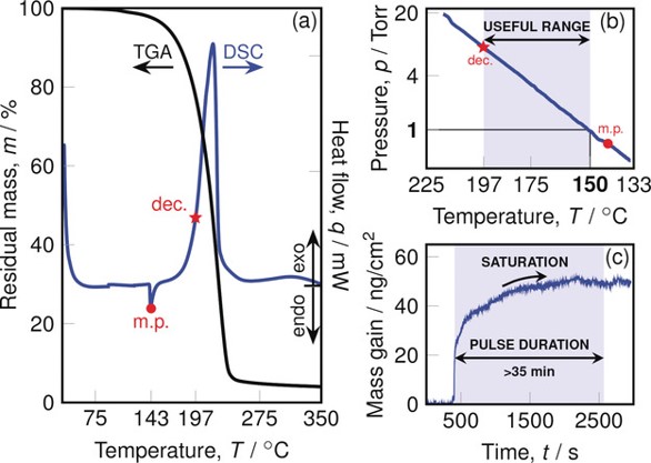
[Press release, Uni Bocum, Germany LINK] Searching for small but stable cobalt compounds, a team has discovered a complex that is relevant for material research and exhibits properties that have not been reported for almost 50 years for a compound alike.

A research team from Ruhr-Universität Bochum (RUB) and Carleton University in Ottawa has manufactured a novel, highly versatile cobalt compound. The molecules of the compound are stable, extremely compact and have a low molecular weight so that they can be evaporated for the production of thin films. Accordingly, they are of interest for applications such as battery or accumulator production. Because of their special geometry, the compound also has a very unusual spin configuration of ½. A cobalt compound like that was last described in 1972. The team published their report in the journal Angewandte Chemie International Edition from 5 May 2020.


A Rare Low‐Spin CoIV Bis(β‐silyldiamide) with High Thermal Stability: Steric Enforcement of a Doublet Configuration. Published under Creative Commons Angew. Chem. Int. Ed., First published: 05 May 2020, DOI: (10.1002/anie.202001518)

The geometry makes the difference

“The few known cobalt(IV) compounds exhibit high thermal instability and are very sensitive towards air and moisture exposure. This impedes their implementation as model systems for broad reactivity studies or as precursors in material synthesis,” explains lead author David Zanders from the Inorganic Materials Chemistry research group in Bochum, headed by Professor Anjana Devi. In his ongoing binational PhD project, which has been agreed upon by Ruhr University and Carleton University by a Cotutelle agreement, David Zanders and his Canadian colleagues Professor Seán Barry and Goran Bačić discovered a cobalt(IV) compound that does not only possess the aforementioned properties but also exhibits an unusually high stability.

Based on theoretical studies, the researchers demonstrated that a nearly orthogonal embedding of the central cobalt atom in a tetrahedrally arranged environment of connected atoms – so-called ligands – is the key to stabilising the compound. This specific geometric arrangement within the molecules of the new compound also enforces the unusual electron spin of the central cobalt atom. “Under these extraordinary circumstances, the spin can only be ½,” points out David Zanders. A cobalt compound with this spin state and similar geometry has not been described for almost 50 years.

Following a series of experiments, the team also showed that the compound has a high volatility and can be evaporated at temperatures of up to 200 degrees Celsius with virtually no decomposition, which is unusual for cobalt(IV).

Promising candidate for ultra-thin layers

Individual molecules of the compound dock onto surfaces in a controllable manner after evaporation. “Thus, the most fundamental requirement of a potential precursor for atomic layer deposition has been fulfilled,” asserts Seán Barry. “This technique has increasingly gained in importance in industrial material and device manufacturing, and our cobalt(IV) compound is the first of its kind that is fit for this purpose.” “Our discovery is even more exciting as the high-valent oxides and sulfides of cobalt are considered to have great potential for modern battery systems or microelectronics,” adds Anjana Devi. Following frequent charging and discharging, electrodes in rechargeable batteries become more and more unstable, which is why researchers are looking for more stable and, consequently, more durable materials for them. At the same time, they also focus on using new manufacturing techniques.

“This binational collaboration, which was initiated by David Zanders, has pooled the creativity and complementary expertise of chemical engineers from Bochum and Ottawa. All this has produced unexpected results and was certainly the key to success,” concludes Anjana Devi.

Original publication

David Zanders, Goran Bačić, Dominique Leckie, Domilola O. Odegbesan, Jeremy Rawson, Jaseon D. Masuda, Anjana Devi, Seàn T. Barry: A rare low‐spin Co(IV) Bis(β‐silyldiamide) with high thermal stability: Steric enforcement of a doublet configuration, in: Angewandte Chemie International Edition, 2020, DOI: 10.1002/anie.202001518

Monday, June 15, 2020

ALD in The Netherlands

The Dutch Vacuum Society – or Nederlandse Vacuümvereniging (NEVAC) – publishes the so-called “NEVAC blad”, a magazine that appears three times a year. The issue for June 2020 just appeared and it is a special issue completely devoted to atomic layer deposition (ALD).

Background information at AtomicLimits: LINK


The front cover of the Special Issue on ALD as published by the Dutch Vacuum Society in the so-called “NEVAC blad”. This issue can be downloaded here.

The 2020 TECHCET Critical Materials Report on CVD, ALD and SOD Metal, High-k and Advanced Dielectric Precursors is out!

The 2020 TECHCET Critical Materials Report on CVD, ALD and SOD Metal, High-k and Advanced Dielectric Precursors is now being sent to customers:
  • Provides market and technical trend information on organic and inorganic precursors, addressing CVD, ALD applications including high κ metal-oxides, barrier layers, metal interconnects, and capping layers, among others.
  • Provides focused information for supply-chain managers, process integration and R&D directors, as well as business development and financial analysts
  • Covers information about key suppliers, issues/trends in the material supply chain, estimates on supplier market share, and forecast for the material segments

Web Link: https://techcet.com/shop/

TECHCET Reports can be Included with CMC Associate Membership, and include Quarterly Updates for most CMR, emailed Analyst’s Alerts of breaking news, and phone consultation with the analyst – Click Here for Membership Info!


EFDS ALD for Industry – postponed – new date: December 02 – 03, 2020

4th Workshop and Tutorial
including industrial Exhibition and Tour of Trumpf Hüttinger GmbH & Co. KG
Web: https://www.efds.org/event/ald2020/
PROGRAM [PDF]
REGISTRATION EXHIBITION [PDF]
TOPICS:
♦ Semiconductor ♦ MEMS and Sensors ♦ Display ♦ Lightning ♦ Barriers ♦ Photovoltaics ♦ Battery ♦ Powder Coating ♦ Medical Applications ♦ Decorative Coatings


CONTENT

A topical workshop with focus on industrialization and commercialization of ALD for current and emerging markets

Atomic Layer Deposition (ALD) is used to deposit ultraconformal thin films with sub-nm film thickness control. The method is unique in the sense that it employs sequential self-limiting surface reactions for growth in the monolayer thickness regime. Today, ALD is a key technology in leading edge semiconductor technology and the field of application in other industries is increasing rapidly. According to market estimates the equipment market alone is currently at an annual revenue of US$ 1.8-1.9 billion (2018) and it is expected to double in the next 4-5 years. In a European context ALD was invented independently twice in Europe (Russia & Finland) and since the last 15 years Germany has grown to become one of the strongest European markets for ALD in R&D, chemicals, equipment and end users.

This year we will organize the 4th Workshop „ALD For Industry“ in South Germany (Freiburg), much closer to the other ALD hubs in continental Europe in France, The Netherlands, Belgium, Italy and Switzerland. ALD for Industry provides the opportunity to get in contact with industrial and academic partners, to learn more about fundamentals of ALD technology and to get informed about recent progress in the field. The Event will focus on the current markets for ALD and addresses the applications in Semiconductor industry, MEMS & Sensors, Battery Technology, Medical, Display, Lightning, Barriers and Photovoltaics.
PARTICIPATION
Ticket Tutorial & Workshop – 790 EUR
Ticket Workshop only – 590 EUR
Ticket Tutorial only – 390 EUR
Student Ticket Tutorial & Workshop – 395 EUR
Student Ticket Tutorial only – 180 EUR
Student Ticket Workshop only – 290 EUR
A certificate is necessary! Please send it via E-mail to info@efds.org.

EVENT LOCATION
ETAGE Tagungscenter an der Messe Freiburg
Emmy-Noether-Straße 2
79110 Freiburg
Tel.: +49 761 3881-3515
etage@fwtm.de
www.etage-freiburg.de
direction

Meaglow delivers large area plasma sources to Okyay Tech

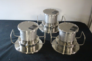
Meaglow has sent 3 of its 4″ diameter large area hollow cathode sources to the equipment manufacturer Okyay Tech, www.okyaytechald.com. This Meaglow design represents a change in the plasma source paradigm of using small area high intensity plasma sources and then diluting the active species over a large area. Instead, these hollow cathode sources have about the same diameter as the substrate, and a very high plasma density over that whole area.


Meaglow has also produced 8″ and 12″ diameter versions of this large area design. Check out the Meaglow website for our other hollow cathode plasma products, www.meaglow.com

Friday, June 5, 2020

Thermal ALD IGZO Properties for LTPO TFTs by NCD

 
LTPS TFTs have been applied to most of the display for smart phones which consume most of the power for their operating because they have high electron mobility showing fast response time even if they have higher power consumption than that of IGZO TFTs,

Recently applications of LTPO (Low Temperature Polycrystalline Oxide) TFTs have been increasing to save the powder consumption of mobile and wearable devices. LTPO TFTs are the device combining LTPS TFTs with fast speed and Oxide TFTs with low leakage current. That is, switching uses Oxide TFTs because of being on/off the light fast and operating uses LTPS TFTs due to changing display rapidly with control of the mount of light.

A lot of smart device manufacturers including Apple are using or will use LTPO displays for their latest smart watches because their power consumption can decrease ~40%. Also, many manufacturers like Samsung and Apple have actively been developing their high-end smart phones equipped with the LTPO displays to make the power usage optimized.


General LTPO Structure and Properties

IGZO thin films used for Oxide TFTs have typically been processed by sputtering, but this method continuously has been showing lots of issues such as their bad thickness and composition uniformity, degradation of the physical and electrical properties due to plasma damage and the stability problem of targets. However using thermal ALD-IGZO, it is possible to deposit high quality thin films because of no plasma damage in process, low process temperature, and atomic scale controllability of thickness and composition.


Thermal ALD IGZO Properties

It is possible to get exact target atomic compositions of IGZO thin films by controlling the ratios of ALD cycle of respective sources in thermal ALD. Therefore this method could show the superior device properties to that by sputtering because it enables to control easily and exactly the most suitable atomic composition for the respective device structure of customers.

NCD has been developing high throughput batch IGZO-ALD system with its creative technology enabled to adapt the target atomic composition for respective devices. NCD could provide the competitiveness of excellent quality and the high productivity for LTPO TFTs including IGZO thin films using Lucida GD Series ALD which could process many and large area substrates at once.


NCD’s LucidaTM GD Series ALD

Source: http://www.ncdtech.co.kr/2018/bbs/board.php?bo_table=eng_board_05&wr_id=51

Tuesday, June 2, 2020

AlixLabs signs agreement to use the lab facilities of NanoLund

AlixLabs signs agreement to use the lab facilities of Sweden’s largest research environment for nanoscience and nanotechnology. At the same time moves in to Ideon Scinece Park in Lund, Sweden.

NanoLund, founded in 1988, is the Center for Nanoscience at Lund University and a Strategic Research Area funded by the Swedish government. Encompassing 55 research groups in the faculties of engineering, science and medicine, more than 130 PhD students.

https://www.nano.lu.se/

AlixLabs (Link)

Wednesday, May 27, 2020

Picosun has new representative in Australia and New Zealand: Australian Vacuum Services

Picosun has new representative in Australia and New Zealand: Australian Vacuum Services


Australian Vacuum Services Pty Ltd     

Email info@australianvacuumservices.com

Phone: +61 (0) 2 8626 6495 / Mobile +61 (0) 4 2361 3086

Web: https://www.australianvacuumservices.com

3/25 Jenner Street | Baulkham Hills | NSW 2153 | Australia                  

ABN 38640001921


Picosun Group’s Strong Growth Continues In 2020 +18,4 % in order intake and accelerating further in 1Q/2020

Picosun Group, the supplier of AGILE ALD (Atomic Layer Deposition) thin film coating technology for global industries, reports strong growth during fiscal year 2018-2019, as a result of Group's strategy to focus on industrial customers. The growth has continued in the first quarter of 2020.

During the fiscal year 1st October 2018 - 31st December 2019, Picosun Group's order intake was 35,9 M€ and turnover 34,2 M€. EBIT was 377 k€. The growth from the previous corresponding 15 months period was +18,4 % in order intake, and +5,5 % in turnover.

Picosun invested over 19 % of the turnover in R&D activities during the last fiscal year. The main R&D activities related to new product developments in line with the new Group strategy. During the period Picosun Group launched many improvements to existing products and services. The most important product launch was PICOSUN Morpher ALD production platform for e.g. MEMS, LED, 5G and power electronics markets, which was launched in July 2019 with positive response from the customers.

Picosun Morpher

Picosun Group has continued its strong growth in the first quarter of 2020, resulting in 10,7 M€ order intake, growth of +64,1% compared to Q1/2019. Turnover grew +36,3 % in the same period. EBIT was 1,2 M€. Despite uncertainty caused by the ongoing coronavirus pandemic Picosun Group expects the growth to continue in the fiscal year 2020, compared to the corresponding period in 2019.

Picosun held its Annual General Meeting on 26th May 2020. Mr. Kustaa Poutiainen continues as the Chairman of the Board. Other Board members nominated by the Annual General Meeting are Dr. Tuomo Suntola, Mr. Juha Mikkola and Mr. Hannu Turunen.

“Despite of the challenges caused by the global COVID-19 pandemic, Picosun's business is continuing strong. Our strategy implementation continues well and has led to positive growth especially in new product sales in the first quarter of this year. We have also hired new personnel and hiring will continue when the corona situation eases off. To support our growth, we are planning to accelerate our investments in product and business development as well as in our facilities and factories. Picosun's success is made of the hard work, dedication and team spirit of our personnel with unmatched expertise in ALD and solid commitment to our customers,” states Mr. Jussi Rautee, CEO of Picosun Group.

Get in touch with AlixLabs - save cost for future leading edge nodes in Semi

For more than 15 years now (since 2004, Samsung 90 nm DRAM) Atomic Layer Deposition (ALD) processing is keeping the advanced chips manufacturable, ensures performance and scaling, and pushing cost down for the consumer. Guess what - now we want to do the same by applying Atomic Layer Etching (ALE) into the leading edge Logic and Memory nanopatterning process flow - helping lithography keeping the overall cost down for you the consumer.

We at AlixLabs invite you to come and chat with us to learn more!


Cost analysis after break down of the Samsung Galaxy S20 Ultra. Credit: TechInsight

Samsung has now introduced of EUV lithography into their 7LPP process

Amazing - Samsung has now introduced of EUV lithography into their 7LPP process used in the Exynos 9825. In a direct comparison, it shows the increased density achieved compared to TSMC’s N7 7.5T 3/3-fin layout

In addition, Samsung has introduced a Self Aligned Diffusion Break (SA DB) that likely reduces performance variation caused by the local layout effect of PMOS transistor.

Source: TechInsight https://www.techinsights.com/blog/techinsights-confirms-samsungs-true-7lpp-process-samsung-exynos-990


With a 27nm fin pitch, this disruptive innovation enables a smaller standard cell height of 270nm while maintaining high drive current with a 3/3-fin layout for both NMOS and PMOS transistors. Credit: TechInsight

Monday, May 25, 2020

AlixLabs ramps up activities and employs Dr. Mohammad Karimi as Principal Scientist

After successfully securing additional soft funding from VINOVA, AlixLabs AB ramps up activities in Lund, Sweden,  and employs Dr. Mohammad Karimi as Principal Scientist. Mohammad Karimi received his PhD in Physics from Lund University in 2020, where he worked on design, nano-fabrication and characterization of novel optoelectronic devices based on semiconductor nanowires. Dr. Karimi has authored and co-authored more than 20 journal publications and conference presentations in the field of solid-state physics and III-V semiconductor devices.

Mohammad Karimi Research Portal and publications at Lund University (LINK)

Dr. Mohammad Karimi as Principal Scientist, AlixLabs AB

Atomic Layer Etching for Nano Device Fabrication at AlixLabs

We provide an ALE-based method of manufacturing nanostructures with a characteristic size below 20 nm.

This is a new method of nanostructure fabrication using the atomic layer etching process, which is inherently a damage-free etch process. The recently discovered etching process selectivity to inclined surfaces, allows to use walls of tapered structures as a mask. The inclined surfaces can be readily fabricated by e.g. dry etching or epitaxial growth, and will provide masking during the atomic layer etching process.

The key Tool for ALE development - An Inductively coupled plasma reactive ion etching (ICP-RIE) system Apex SLR from Advanced Vacuum Systems AB. The system is designed for controlled nanoscale etching of Si, SiO2, Si3N4, W, Mo and polymers (resists) with fluorine-based chemistry. Unprotected surfaces of the following materials are not allowed: glasses, noble metals (Au, Ag, Pt, Cu, Pd), heavy metals (Cd, Pb, Zn) and certain types of polymers (e.g. silicones). In total, 8 process gases are presently available: SF6, CHF3, CF4, C4F8, Ar, O2, H2, N2. LINK

The inclined surfaces can be readily fabricated by e.g. dry etching or epitaxial growth, and will provide masking during the atomic layer etching process. This process therefore provides access to fabrication of extremely small structures in a very precise and efficient way.

AlixLabs is a user at Lund Nanlo Lab, Lund University, Sweden

Lund Nano Lab (LNL) is an open research facility that is available to both academic research groups, start-up and company users. Our world-class clean room facility is equipped with state-of-the-art semiconductor processing and metrology equipment.

  • ISO 5 and ISO 7 cleanroom facility for cutting edge nano- and micro-fabrication
  • 24/7 access for accredited academic research and company users
  • Fabrication and analysis of structures on the micro- and nanometer-scale
  • Wide range of equipment for Growth, Lithography, Deposition, Etch and Characterisation
  • Centre of excellence for Epitaxial growth of III-V materials
  • Industrial product development and prototype testing
  • Staffed by expert equipment and process experts available to provide user training

Lund Nano Lab is one of the main resources within NanoLund and provides support to research groups in strategically important areas of research such as:

  • Nanowire growth and material science
  • Fundamental and device physics, electronics and photonics
  • Nano-bio and life science
  • Exploratory nanotechnology
  • Growth and physics of new materials
  • Nanowire-based photovoltaics
  • Processing of nanoelectronic devices and circuits


Thursday, May 21, 2020

A GLOBAL DIGITAL CONFERENCE ON PARTICLE ATOMIC LAYER DEPOSITION [PALD]

Forge Nano and over 20 speakers are ready for the First Annual PALD Summit LIVE May 21st, a FREE virtual event. Please sign in today for the LIVE Q&A schedule with all our speakers! Then come back and view the content until June 1st.

Web: LINK


Reuters: Samsung Electronics builds sixth domestic contract chip-making line

Samsung breaks the ground for building its 6th domestic production line in Pyeongtaek city to expand its 5 nm chip-production capacity, using EUV technology: Samsung has planned to expand its production of logic chips for mobile phones and computers as it looks to cut reliance on the volatile memory chip sector. The new production line is targeted to be operational by 2H21. Last year, Samsung announced to invest 133 trillion won ($107.97 billion) in non-memory chips through 2030, comprising 73 trillion won for domestic R&D and 60 trillion won for production infrastructure.

Source: Reuters LINK

----------
By Abhishekkumar Thakur

PALD2020 Sundqvist - Roating Drum ALD and LPCVD

The Americans forgot that we have a holiday today and in Germany celebrate something called Männertag (see link below). For all you Europeans that may have fallen asleep after midnight or Germans that had one too many beers - here my presentation upfront at the PALD Summit:


Roll-to-roll ALD for lithium-ion batteries by Beneq R2R

In this talk with Dr. Tommi Kääriäinen of Beneq they discuss how ALD can help solve performance and safety issues for ever-evolving lithium-ion battery products. Specifically they compare roll-to-roll ALD, a tool design pioneered by Beneq, with particle ALD technology.


Don´t miss to register and tune in to Forge Nanos PALD Summit today!


Tuesday, May 19, 2020

Hafnium, Zirconium: Australian Strategic Materials a step closer to completing commercial pilot plan

Recent semiconductor materials related trade issues between Japan and South Korea have led South Korea to secure alternative sourcing of photoresists and metals for their semiconductor industry. This includes essential minerals for hafnium and zirconium ALD precursors that are used in the manufacturing of DRAM and Foundry logic at SK Hynix and Samsung fabs.

Besides the tension with Japan, China's dominance in the supply of zirconium chemicals and materials has highlighted the additional risk in the critical materials supply change for its important semiconductor and high tech industries.

One such action has been setting up a pilot plant in South Korea for hafnium and zirconium metal in joint development with Australias Alkane and its subsidiary Australian Strategic Materials (ASM). The joint undertaking has now moved to the next phase for a commercial operation of a pilot plant as reported by Alkaine below.

Australian Strategic Materials a step closer to completing commercial pilot plan

Australian Strategic Materials (ASM), a wholly owned subsidiary of Alkane Resources is getting closer to completing the construction of a commercial pilot plant facility in South Korea that will enable critical metal oxides, including zirconium and hafnium, to be converted into metals in clean, carbon-free way.

As the Covid-19 pandemic continues to highlight weaknesses in critical minerals supply chains globally, ASM has confirmed in Alkane Resources' quarterly recently it has received interest in both potential future supply and partnership from a number of parties in South Korea and elsewhere. ...

Read more.


Read more about previous blog about the Alkane Dubbo project in New South Wales, Austrailia:

The Dubbo Project - The High-k mine in Dubbo, NSW Australia

Hafnium product breakthrough consolidates Dubbo Project business case

China’s water crisis stems the flow of zirconium and rare earths for global industries

Alkane Resources reports that zirconium oxychloride (ZOC) prices are up 40% since January 2017


Monday, May 18, 2020

SEMICON West will be a virtual event July 20-23

The microelectronics annual conference, and the flagship event for the semiconductor industry, was due to be held at the Moscone Center, San Francisco, California, but due to the coronavirus (Covid-19) pandemic it has now moved to a virtual format.


Visitors will hear from, and interact with, visionaries and executives from across the microelectronics supply chain and its markets.
Presentations will feature emerging applications that demand the industry’s design and manufacturing expertise. Virtual exhibit booths throughout the detailed, interactive exhibit hall provide the opportunity to network and gather insights just like on a physical show floor.
Attendees can stop by SMART technology pavilions and exhibitors’ booths to view video content, download informative product information, and converse with supplier representatives.
“This will be the deepest, most extensive online global industry event this year,” said David Anderson, President of SEMI Americas and host for the gathering.
“As a virtual conference, SEMICON West 2020 allows us to offer our customers – large and small – A-list speakers and a full exhibition experience, with all the content, interactions and networking opportunities of a physical show – without the associated costs and time of travel.”
Attendees can also join technical sessions, participate in one-on-one or group meetings, and interact with colleagues and industry representatives in networking areas.
Registration opens May 18, 2020; a notification form and detailed information on the event are available at www.semiconwest.org.

ACM Research Enters Dry Processing Market with Launch of CVD/ALD Ultra Furnace

  • ACM’s First Furnace Product Targets LPCVD Initially, Oxidation, Annealing and ALD in Future
  • ACM Research intends to target customers in China initially, before expanding the offering of the Ultra Furnace into Korea and Taiwan later.
  • ACM delivered the first Ultra Furnace tool to a key logic customer’s manufacturing facility in China in early 2020. This tool targets LPCVD, and has been installed in a production environment to begin qualification.

FREMONT, Calif., April 28, 2020 (GLOBE NEWSWIRE) -- ACM Research, Inc. (“ACM” or the “Company”) (NASDAQ:ACMR), a leading supplier of wafer cleaning technologies for advanced semiconductor devices, today unveiled the Ultra Furnace, its first system developed for multiple dry processing applications. Initially optimized to deliver high performance for low-pressure chemical vapor deposition (LPCVD), the Ultra Furnace also leverages the same platform to be used for oxidation and annealing processes, as well as for atomic layer deposition (ALD). This achievement represents a two-year collaboration between ACM’s R&D teams located in China and Korea.


“Advanced technology nodes present ongoing challenges that require innovation from the capital equipment suppliers. This demanding environment provides significant opportunities for ACM,” explained Dr. David Wang, CEO of ACM Research. “Continuous innovation is in our DNA. We saw a market need that could benefit from our technology, and expanded our reach into a new market segment. The addition of the Ultra Furnace to ACM’s established portfolio of wet processing tools, expands our opportunity by providing an integrated solution to our customers’ advanced products.”

“The Ultra Furnace product is the result of collaboration between our talented experts in China and Korea to develop differentiated technology,” stated YY Kim, CEO of ACM Research Korea. “ACM’s team in Korea was established to complement the talents of our world-class Shanghai team, accelerate our time to market, and provide outstanding technical support to our local customers.”

Deposition processes utilize process gases at a high temperature to react with each other on a silicon wafer, forming a silicon oxide or nitride layer on the wafers. The Ultra Furnace system is intended for batch processing of up to 100 12-inch (300mm) wafers. The innovative system design combines newly developed hardware that improves durability, with the company’s proven software technology and a proprietary control system and algorithm. This enables the tool to provide stable control of pressure, gas flow rate and temperature.

While the Ultra Furnace system targets LPCVD processes, with a few changes to the components and layout, each tool can address other target applications. About 85 percent of the hardware configuration remains unchanged, so the alterations for the new application can be achieved efficiently.

ACM Research intends to target customers in China initially, before expanding the offering of the Ultra Furnace into Korea and Taiwan later. ACM delivered the first Ultra Furnace tool to a key logic customer’s manufacturing facility in China in early 2020. This tool targets LPCVD, and has been installed in a production environment to begin qualification.