Friday, April 17, 2020

Volatile ALD & CVD Magnesium precursors for non-volitile memory and flexible display applications


The escalating struggle with further scaling of integrated circuit chips, on account of certain feature sizes in advanced chips gradually hitting atomic dimensions, has compelled the semiconductor industry to become more welcoming to new materials as a possible solution to continued PPAC (Power-Performance-Area-Cost) improvement. Traditionally not so popular in the semiconductor industry, Magnesium (Mg) is being explored for use in various related applications due to the fact that it forms semiconductor compounds with oxygen, sulfur, selenium, and tellurium.

For example, Magnesium Oxide (MgO) is a semiconductor with a wide band-gap and semi-insulating properties. A very thin semi-insulating MgO layer between two metallic ferromagnetic layers is used as a “magnetic tunnel junction”. Magnetic tunneling junctions (MTJs) based on the CoFeB/MgO/CoFeB layer have received great attention as a promising candidate for future spin logic devices. Among various applications of MTJs, spin-transfer-torque magnetic random access memory (STT-MRAM) is emerging as a strong candidate as a next-generation nonvolatile memory due to its simple integration scheme, low voltage operation, and high speed. To fulfill certain critical requirements of 3D MTJ based sub-20 nm, high-density STT-MRAM, Samsung Advanced Institute of Technology (SAIT), Korea, has recently investigated both thermal and plasma-enhanced ALD for depositing a MgO tunnel barrier using bis(cyclopentadienyl)magnesium precursor under the scope of the Industrial Strategic Technology Development Program (10041926, Development of high-density plasma technologies for the thin-film deposition of nanoscale semiconductors and flexible-display processing) funded by the Ministry of Knowledge Economy (MKE, Korea). (Link)


Figure 1. TEM images of (a) Thermal ALD MgO, (b) PE-ALD MgO grown at 300 °C on a CoFeB layer

Recently, Panasonic Corporation, Japan, together with the National Institute of Material Science, Japan, reported ALD based Magnesium Phosphate (MgPO) thin-films as magnesium-ion conducting solid-state electrolytes that are considered to be promising candidates for future energy storage and conversion devices. The deposition was carried out at lower deposition temperatures, ranging from 125 to 300 °C, using bis(ethylcyclopentadienyl)magnesium. (Link)

Apart from semiconductor and energy storage applications, Mg is also an interesting candidate for astronomical and optical applications. For example, recent NASA missions that make observations in the ultraviolet, such as the Hubble Space Telescope and the Galaxy Evolution Explorer, employed primary mirrors coated with aluminum and further protected by thin films of Magnesium Fluoride (MgF2). Therefore, the Jet Propulsion Laboratory, California Institute of Technology, under a contract with NASA, reported ALD of MgF2 using bis(ethylcyclopentadienyl)magnesium supplied by Strem Chemicals, Inc. (Link)
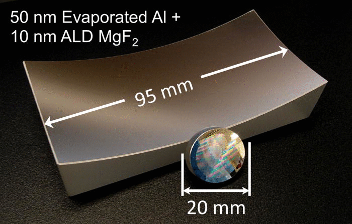


Figure 2. Photograph of a concave mirror and convex diffraction grating for a next-generation UV instrument prototype coated with electron beam evaporated aluminum and a protective coating of 10 nm ALD MgF2 deposited at 150 °C.

Strem Chemicals, Inc., a leading fine chemicals supplier, headquartered in Newburyport, Massachusetts, USA, offers the most preferred precursors worldwide for ALD of Mg-based compounds, i.e, bis(ethylcyclopentadienyl)magnesium [Mg(CpEt)2] (catalog number 12-0510). The colorless to pale yellow liquid phase precursor with a density of 0.95 g/cm3 at 20 °C and vapor pressure of 0.0315 Torr is also sold by Strem Chemicals as pre-packed in cylinders:

§  98-4006: Bis(ethylcyclopentadienyl)magnesium, min. 98%, 12-0510, contained in 50 ml Swagelok® cylinder (96-1070) for CVD/ALD

§  98-4010: Bis(ethylcyclopentadienyl)magnesium, min. 98%, 12-0510, contained in high-temp 50 ml Swagelok® cylinder (96-1071) for CVD/ALD
 
About Strem Chemicals: Strem is an employee-owned fine chemicals supplier, manufacturing and marketing high-quality specialty chemicals for more than half-a-century. They provide custom synthesis and FDA inspected current good manufacturing practice (cGMP) services to its clients from academia as well as industry and also to government R&D labs. What distinguishes Strem from the other chemical suppliers are its ISO 9001 Quality Management System (QMS) standard and documenting procedures including for example “Color and Form” for every product as listed in the product details as a quality indicator for researchers. This helps Strem deliver precursors with a minimum metals purity of  99%, with some  some metal precursors attaining as high as 99.9999% metal’s purity. Strem offers over 5,000 specialty products in the area of metals, inorganics, organometallics, and nanomaterials. Strem’s product range includes:


Products Mentioned in this Blog:
12-0510: Bis(ethylcyclopentadienyl)magnesium, min. 98% (114460-02-5)
98-4006: Bis(ethylcyclopentadienyl)magnesium, min. 98%, 12-0510, contained in 50 ml Swagelok® cylinder (96-1070) for CVD/ALD
98-4010: Bis(ethylcyclopentadienyl)magnesium, min. 98%, 12-0510, contained in high-temp 50 ml Swagelok® cylinder (96-1071) for CVD/ALD


Related Product Lines & Resources:


----------
Promotional blog written and researched by Abhishekkumar Thakur and Jonas Sundqvist, BALD Engineering AB
 

Friday, April 10, 2020

AVS ALD/ALE2020 has been cancelled due to the Coronavirus pandemic

What a pain for us all, and especially for the organizers, because of the ongoing Coronavirus pandemic, it is unfortunate to report that the AVS-ALD2020 conference Gent, Belgium has been canceled.

AVS ALD/ALE 2020 web page and announcement: https://ald2020.avs.org/

According to information from the organizers, most likely, an online event will be organized with "virtual" plenary sessions and a possibility to upload a digital version of the presentation/poster. AVS is currently looking into this.

So 2020 turns out to be a challenging year for us all, if you want to get results or ALD products out there, please feel free to contribute to this blog. So if you have just published a paper, have a new ALD chamber on the market or a funky precursor - send it to me, and I will post it here ready for sharing in social media - it is for free!

Stay positive! Stay safe eveyrone! ALD - Let´s get it rolling!
Jonas 


Monday, April 6, 2020

White Paper: Atomic Layer Deposition for Quantum Devices

As the transistor gave rise to the information age, quantum technology has the potential to be the next great leap forward. Quantum technology is the application of quantum physics for real-world applications, such as quantum computing, sensing, navigation and communication.

Conventional methods for depositing superconductors include sputtering, pulsed laser deposition (PLD), and chemical vapour deposition (CVD). However, these methods can suffer from drawbacks including a lack of thickness control, poor uniformity and high impurity content.

Atomic layer deposition (ALD) is much more beneficial for thin-film deposition due to its ability to produce films with high purity, precise thickness control, conformal coating in high aspect ratio structures, and uniformity over large-area substrates.
 
 Download: LINK

Thursday, April 2, 2020

TSMC hit by 3nm delay fears over Covid-19 Lock-downs

TSMC is on schedule with its 5 nm process plan, but its 3 nm trial production may get delayed: The world's largest contract chipmaker is planning to launch mass production of its 3 nm process sometime in 2022, and media reported Monday that installation of production equipment in its 3 nm wafer fab in Tainan will be delayed to October from June this year, which will delay its trial production set for 2021. The COVID-19 escalation has hit Europe, and [Netherlands-based] ASML Holding, which is TSMC's major production equipment supplier, has been affected by a lockdown. It is understandable that the progress of TSMC's new technology has been affected.

Below a comparison of the Covid-19 daily new confirmed deaths, which is the only comparable parameter to use due to different testing capabilities and frequencies, in time and nation to nation. As can be seen the situation in Asian is under control after the gotten hit by the first wave of the Coronavirus. The European situation is stabilizing: Italy, Netherlands, Germany France, others look similar and are flattening the curve. In The USA situation is escalating. Many nations in Europe are forecasting a lift of Lockdown in May but are very careful, as an example Germany will decide in 19 April how to proceed according to Chancellor Dr. Angela Merkel.

BALD Engineering AB continues to monitor the Covid-19 situation due to lockdowns that affect the  the semiconductor industry – Stay Safe!

Google Finance (2020-04-02, 10:39 CET)

Sources:

Taiwan shares edge lower, TSMC hit by 3nm delay fears

Our World of data: https://ourworldindata.org/coronavirus

-----------
By Abhishekkumar Thakur, Jonas Sundqvist

Tuesday, March 31, 2020

Electronics Gas Market to reach $8.0B by 2024 despite expected COVID-19 impacts

San Diego, CA, March 30, 2019: TECHCET announced that the semiconductor fabrication gases market is forecasted as net positive in revenue growth for Q1, despite COVID-19. Although economic uncertainties for the remainder of the year may slow growth, current indications from the materials supply-chain look like "business as usual."

"Suppliers say that orders are strong," summarizes TECHCET President and CEO Lita Shon-Roy. "However, concerns exist that fabs may start to stock-pile materials to mitigate the possibility of interruption, especially from US suppliers that are now in the throes of the COVID-19 spread."

One recent positive for chip fabs is helium availability, where non-semiconductor demand is expected to ease. Given the COVID19 situation, medical and recreational (party balloons) helium demand will decline, allowing for the current shortage in the semiconductor supply-chain to mitigate sooner than expected. Major new sources like Gazprom, Arzew, and Qatar are scheduled to finally come online later this year.

TECHCET is also tracking potential disruptions in raw materials for critical gases—e.g. germanium for GeH4 and GeF4, fluorspar for HF, tungsten for WF6—has been minimal, because many Chinese suppliers had prepared safety stock for the Lunar New Year break.

Air Liquide, Air Products, Linde, Messer, and SK Materials have all announced increases in global production of gases. The market for both bulk- and specialty-gases is forecasted to grow from US$5.4B in 2019 to US$8.0B by 2024, as shown in the figure below. However, uncertainties exist for 2020 where demand may soften as a result of a prolonged impact of COVID19 on global economies.

TECHCET’s Critical Materials Report™ on Electronic Gases includes market landscape analysis and company profiles of Air Liquide, Linde, TNSC-Matheson, Versum Materials, Air Products, Showa Denko, SK Materials, Air Water, Hyosung, Peric, Kanto Denka Kogyo, and more. To purchase Report go to: https://techcet.com/product/gases/ 

Monday, March 30, 2020

Photonics for optical data transmission with Picosun’s Erbium ALD solutions

ESPOO, Finland, 30th March 2020 – Picosun Group reports excellent results in development of state-of-the-art photonics with its ALD (Atomic Layer Deposition) equipment and solutions.


Photonic devices such as waveguide amplifiers and lasers are central components in optical data transmission, a key technology realizing our modern, connected, information-driven society.

Silicon-integrated photonics take the technology one step further, enabling a whole new generation of microelectronics where optical solutions overcome some of the key challenges of conventional technologies.

Erbium-doped waveguide amplifiers and lasers are the most potential candidates for signal generation and amplification for telecommunication wavelengths. To reach the maximum performance of these devices, the amount and spatial distribution of dopant erbium atoms in the host material must be carefully optimized and controlled. This is where ALD shows its unique strength and beauty.

At Aalto University, Finland, Picosun’s customer Prof. Zhipei Sun’s group at the Finnish national infrastructure Micronova, and his international collaborators, have now used Picosun’s ALD technology to manufacture erbium-based silicon-integrated waveguide amplifiers with world-record performance(*).

“Silicon-integrated photonics, already employed by the leading companies in the field, are the future of microelectronics. We are very pleased of the performance of our PICOSUN® ALD equipment and the excellent quality of the Er:Al2O3 waveguide amplifiers manufactured with it. Customer support and consultancy from Picosun have always been there when we need it. ALD process is CMOS-compatible, further facilitating the integration of our waveguides into commercial chip production,” states Dr. John Rönn, the leading author of the results, from the Department of Electronics and Nanoengineering at Aalto University.

”ALD has been enabling disruptive future technologies since its invention. Picosun is happy to work with the leading experts in the field, such as our esteemed customers at the Aalto University. Our ALD solutions provide them the means to realize their groundbreaking work to develop yet more advanced communications and data transmission technologies for more connected, open, and integrated global society,” continues Mr. Edwin Wu, CEO of Picosun Asia Pte. Ltd

(*) The results were published in the journals ACS Photonics 3, 2040-2048 (2016) and Nature Communications 10, 432 (2019).

Covid-19 Update - European/US situation benchmarked with South Korea

Here is the latest plot that I make on the Covid-19 situation (Monday morning 2020-03-29 data) plotted as casualties per 1 million inhabitants for a number of countries in Europe + USA and benchmarking with South Korea. You can follow these and the dicussionon LinkedIn.

Soon there will be a podcast interview in Swedish English radio available on Spotify (LINK)


Saturday, March 28, 2020

Call for abstracts, ALD Applications ECS PRiME October 4-9, 2020 | Honolulu, Hawaii

PRiME 2020 Topic Close-up: Atomic Layer Deposition Applications 16
Symposium focus: This symposium contains cutting edge research results on applications in Atomic Layer Processing and will focus on a variety of applications of ALD and other atomic layer-by-layer processing (like etching and cleaning). 


The organizers would like to invite contributions to the following topics:
  • Semiconductor CMOS applications: development and integration of ALD high-k oxides and metal electrodes with conventional and high-mobility channel materials;
  • Volatile and non-volatile memory applications: extendibility, Flash, MIM, MIS, RF capacitors, etc.;
  • Interconnects and contacts: integration of ALD films with Cu and low-k materials;
  • Fundamentals of ALD processing: reaction mechanisms, in-situ measurement, modeling, theory;
  • New precursors and delivery systems;
  • Optical and photonic applications;
  • Coating of nanoporous materials by ALD;
  • MLD and hybrid ALD/MLD;
  • ALD for energy conversion applications such as fuel cells, photovoltaics, etc.;
  • ALD for energy storage applications;
  • Productivity enhancement, scale-up, and commercialization of ALD equipment and processes for rigid and flexible substrates, including roll-to-roll deposition;
  • Area-selective ALD;
  • Atomic Layer Etching (‘reverse ALD’) and related topics aiming at self-limited etching, such as atomic layer cleaning, etc.
Confirmed invited speakers:
  • Area-selective ALD processes for dielectrics, Sumit Agarwal, Colorado School of Mines, USA
  • Reactions on metal surface and diketone induced by gas cluster ions during Atomic Layer Etching, Noriaki Toyoda, Hyogo University, Japan
  • Molecular Layer Etching, Jeffrey Elam, Argonne National Laboratory, USA
  • Ga2O3 phase control and heterojunctions using PE-ALEpitaxy, Virginia Wheeler, US Naval Research Labs, USA
  • ALD for battery technologies, Arrelaine Dameron, Forge Nano, USA
  • ALD materials for solar fuels, Paul McIntyre, Stanford University, USA
  • Investigations into molecular layer deposition of conjugated amine polymers, Matthias Young, Univ. of Missouri, Columbia, USA
  • Functional Metal Oxides in Perovskite Solar Cells, Yu Duan, Jilin University, Changchun, China
  • In-situ and combinatorial techniques for spatial ALD, Kevin Musselman, University of Waterloo, Canada
  • Benefits of Spatial ALD compared to batch and single-wafer ALD methods, David Omeara, TEL Technology Center, America, USA
  • Surface thermolysis of ALD precursors and its implications for deposition, Xinwei Wang, Peking University, China
  • Recent developments in Materials characterization for the CMOS industry, Paul van der Heide, Imec, Belgium
  • MLD of metal-organic thin films with tuneable conductance for neuromorphic computing applications, Mikko Nisula, University of Ghent, Belgium
  • ALD of Phase Change and Threshold Switching Materials for Next-Generation Nonvolatile Memory Devices, Karl A. Littau, Intermolecular-EMD Group, USA
  • Coatings of (TiO2) Nanotube Layers, Jan Macak, University of Pardubice, Czech Republic
  • Recent development of various In-precursors and InOx related oxide semiconductor TFTs via ALD, Jin-Seong Park, Han Yang University, Korea

Deadline for submitting abstracts:
April 17, 2020

Thursday, March 26, 2020

NCD supplied two Lucida M300 ALD systems for R&D to KANC

NCD has recently supplied 2 Lucida M300PL ALD systems to KANC. Lucida M300PL-O is the equipment for oxide deposition with Ozone and Plasma process, and Lucida M300PL-M is that for metal deposition with Plasma process.

These wafer process equipment have the specification below

1) System: Lucida M300PL-O, Lucida M300PL-M

2) Substrate: Wafer 300mm

3) Deposition Materials:

- Lucida M300PL-O: Al2O3, TiO2, ZrO2, ZnO, HfO2, Ta2O5

- Lucida M300PL-M: Co. Ru, W, Ir, TiN, TaN

KANC, which is the most prestigious institute of Korea on nanotechnology, is using Lucida M300PL to investigate cutting edge semiconductor development and promising applications in MEMS and IoT. So it will be expected that these systems will contribute very much to the development of high-end nanotechnology.

NCD will do best to be the best ALD equipment company with continuous R&D efforts. 


< Lucida M300PL ALD >

Wednesday, March 25, 2020

ALD - Let´s get it rolling

First of all, an apology to all readers of the BALD Engineering ALD News Blog. There have been less than usual activities on the blog for the last couple of weeks. Recently I decided to quit my good safe job at Fraunhofer to start working as an ALD consultant and Blogger full time under BALD Engineering AB (LINK) and first and fore and most for TECHCET LLC CA (LINK). 

In February, I practiced my new life during our 2 week family winter holiday in Colombia and took some beautiful pictures from my different home offices on that fantastic trip.
 
Home Office at Playa Blanca, Isla Baru, Colombia
 
More recently, however, the Corona crisis hit us all, and I think everyone has gone through a time to adapt to a different type of life under these circumstances, and my romantic picture of the home office has changed a bit for now.

The first thing that hit me was postponing workshops and conferences, and I think many of you were looking forward to the ALD events in 2020. Here is a status overview of events I am either involved in or planned to join.

AVS ASD 2020 in Stanford, USA - will be moved (LINK)

EFDS ALD for Industry 2020 in Freiburg Germany - is moved to 2-3 December (LINK)

Novel High-k Workshop 2020 in Dresden, Germany - cancelled (LINK)
 
The Critical Materials Conference CMC2020 in Hillsboro, USA  - is moved to (LINK)

AVS ALD/ALE 2020 in Ghent Belgium - still scheduled to take place pending the situation (LINK)

Please let me know which 2020 events in addition to these that should be tracked here!

ALD - Let´s get it rolling

With this as a background, I decided that I need to get things moving again and that is why I now offer all of you who planned to participate in any of these or other ALD events 2020 to send me research news and /or promotional material fro your research or commercial products that you would like to get out there to the ALD community published here at this blog and shared in social media. 

Please send the material to me, and we will format it for the blog format and push it out to the ALD community - it is for free!

Two blogs (Strem and Beneq) are already in the pipeline, and I hope to see more from you - Stay Safe!

Contact: jonas.sundqvist@baldengineering.com


Typical back yard Hostel Home Office. Medellin, Colombia.

Hostel at the Caribbean, Always good coffee in Colombia!
 

Picosun reinforces local operations to ensure customer satisfaction during the COVID-19 epidemic

ESPOO, Finland, 23rd March 2020 – Picosun Group’s first priorities are customer satisfaction and health and wellbeing of the Group’s employees and customers. Picosun takes extremely seriously the global threat posed by the COVID-19 novel coronavirus epidemic and follows the rules set by governments and WHO. As the epidemic restricts global traveling, the importance of local offices and subsidiaries close to the customers is of utmost importance.


The last years have been the time of rapid growth and expansion for Picosun. Strong emphasis has been put on new recruitments especially on the service and support sector. Trained and qualified staff of service engineers are on call at the Group’s US locations in Texas, Arizona, and California and Asian locations in Japan, China, Taiwan, and Singapore. Dedicated sales and support personnel in Germany and France are available for the Group’s European customers. Local process support is also available on each continent.

At Picosun’s Finnish headquarters and local offices employees are encouraged to remote work from home whenever possible. Meetings are arranged virtually via video links and online platforms and inviting external visitors to the company’s premises is minimized to bare necessities. Cleaning of the premises and other hygiene measures have been intensified. All recruitment interviews are conducted remotely.

Despite of the challenging times, Picosun’s customer projects and deliveries continue. Process support and applications consultancy is always available from our Ph.D. level experts, and our Helpdesk serves 24/7 at support@picosun.com. Delivered PICOSUN® ALD system installations and commissioning, as well as customer support on-site, are taken care of by local Picosun offices with their trained and experienced staff.

“All of us here at Picosun wish good health and safety to everybody in this difficult and unexpected situation. In times like this, collaboration is the key to success and speedy recovery. Our business continues and we will put all our effort in sustaining the high level of quality that is the trademark of Picosun. We will further intensify our efforts to bring the benefits of ALD to medical industry. ALD is the very technology that enables our modern, mobile, data-driven and interconnected global society. Now is the time when this society can truly work together for better future,” says Jussi Rautee, CEO of the Picosun Group.

For more information regarding your projects or deliveries, please contact your respective Picosun sales or support contact person. For quotations for our ALD equipment and solutions, or process demo, please contact sales@picosun.com or coating@picosun.com, respectively.

As several expos and conferences the Group is sponsoring or exhibiting at have been postponed, please see the new dates in our event calendar on our website. Picosun is looking forward to meeting you all again later this year in good health and spirits!

Wednesday, March 4, 2020

Lam’s new Sense.i Etch platform delivers industry-leading output and innovative sensor technology

  • Lam Research (NASDAQ:LRCX) introduces the Sense.i tool, which etches finer 3D details on silicon wafers for chips.
  • The Sense.i platform enables the critical etch capabilities required to continue advancing uniformity and etch profile control for maximizing yield and lowering wafer costs
  • 3D features can help Lam customers like Samsung and SK Hynix put more memory capacity into small areas such as smartphones.
FREMONT, Calif., March 03, 2020 (LINK) -- Lam Research Corp. (Nasdaq: LRCX) today announced the launch of a completely transformed plasma etch technology and system solution, designed to provide chipmakers with advanced functionality and extendibility required for future innovation. Lam’s groundbreaking Sense.i™ platform offers unparalleled system intelligence in a compact, high-density architecture to deliver process performance at the highest productivity, supporting logic and memory device roadmaps through the coming decade.

youtube.com


With core technology evolved from Lam’s industry-leading Kiyo® and Flex® process modules, the Sense.i platform enables the critical etch capabilities required to continue advancing uniformity and etch profile control for maximizing yield and lowering wafer costs. As dimensions shrink and aspect ratios increase, the Sense.i platform is designed to support future technology inflections.

Powered by Lam’s Equipment Intelligence® technology, the self-aware Sense.i platform enables semiconductor manufacturers to capture and analyze data, identify patterns and trends, and specify actions for improvement. Sense.i also features autonomous calibration and maintenance capabilities that reduce downtime and labor costs, and delivers machine learning algorithms that allow the tool to self-adapt to minimize process variations and maximize wafer output.

The Sense.i platform has a revolutionary space-saving architecture that will help customers meet their future wafer output targets by producing more than a 50% improvement in etch output density. As semiconductor manufacturers develop smarter, faster, and denser chips, processes are rapidly growing in complexity and number of steps. This requires a greater number of process chambers in a fab and reduces total output for a given floor space. The Sense.i platform’s smaller footprint benefits either a new fab build or a fab undergoing a node-to-node technology conversion.

“Lam is introducing the most innovative etch product that has been developed in the last 20 years,” said Vahid Vahedi, senior vice president and general manager of the Etch product group at Lam Research (LRCX). “Sense.i extends our technology roadmap to meet our customers’ next-generation requirements while solving the critical cost scaling challenges they’re facing in their business. With more than four million wafers processed on Lam etch systems every month, Lam has an installed-base that provides extraordinary learning to innovate, design, and produce the best tools for semiconductor manufacturing.”

Thursday, February 27, 2020

Picosun delivers multiple production ALD systems to Asia for solid state lighting device manufacturing

ESPOO, Finland, 26th February 2020 (LINK) – Picosun Group, Finland-based, global provider of advanced Atomic Layer Deposition (ALD) thin film coating solutions, has been chosen by a major Asian customer to deliver significant ALD production capacity for manufacturing of solid state lighting devices. 

The PICOSUN® P-300BV ALD system is specially designed for production of LEDs, discrete devices, and MEMS devices such as print heads, sensors, and microphones.
 
Solid state illumination technologies are the future of lighting. Running on much lower power than other lighting devices and lasting much longer, they save both resources and environment. As small, compact and light-weight they are also simple to use in remote locations such as rural areas in developing countries, thus providing safe and easily powered lighting for example for children to study or health care stations to operate.

Picosun wants to introduce ALD to applications where it can improve both people’s quality of life and the state of the environment. Indeed, ALD is an ideal technology to enable various sustainable solutions, not only in lighting but in various other industries. In many cases, replacing thick, lower quality coatings with ultra-thin but superior quality ALD films leads to both material and energy savings and longer end product lifetime. Picosun’s equipment design, refined to top-notch performance through decades of cumulative experience in the field, ensures that no matter what industry, an optimal coating solution can always be found from the company’s portfolio.

“ALD films enhance the performance and lengthen the lifetime of solid state lighting devices. Our PICOSUN® P-300BV ALD system is specifically designed for these applications. It combines fast batch production capacity with vacuum loading for the highest ALD film quality and purity. We are happy to be chosen as the ALD technology provider for our esteemed customer. A facility of multiple P-300BV ALD tools that shall be installed in their premises will significantly strengthen our position in this market. For the end users, our ALD solutions enable flexible, power-saving and environmentally friendly lighting solutions with superb brightness and long life,” says Mr. Edwin Wu, CEO of Picosun Asia Pte. Ltd.