Friday, January 24, 2020

Program release - EFDS ALD for Industry 2020 in Freiburg, Germany (March 31-April 1)

A topical workshop with a focus on industrialization and commercialization of ALD for current and emerging markets

Atomic Layer Deposition (ALD) is used to deposit ultraconformal thin films with sub-nm film thickness control. The method is unique in the sense that it employs sequential self-limiting surface reactions for growth in the monolayer thickness regime. Today, ALD is a critical technology in leading-edge semiconductor technology, and the field of application in other industries is increasing rapidly. According to the market estimates, the equipment market alone is currently at an annual revenue of US$ 1.8-1.9 billion (2018), and it is expected to double in the next 4-5 years. In a European context, ALD was invented independently twice in Europe (Russia & Finland), and since the last 15 years, Germany has grown to become one of the strongest European markets for ALD in R&D, chemicals, equipment, and end-users.
Keynote: Prof. Henrik Pedersen, Linköping University
Tutorials by : Bochum University, Lund University, Uppsala University, Oxford Instruments, TECHCET / Fraunhofer IKTS 
Presentations by: Air Liquide, BASF, CEA Leti, Encapsulix, Picosun, Veeco, Sentech, Beneq, Fraunhofer IPMS-CNT, Positive Coating, ATLANT 3D Nanosystems, Fraunhofer FMD 
This year we will organize the 4th Workshop „ALD For Industry“ in South Germany (Freiburg), much closer to the other ALD hubs in continental Europe in France, The Netherlands, Belgium, Italy, and Switzerland. ALD for Industry provides the opportunity to get in contact with industrial and academic partners to learn more about the fundamentals of ALD technology and to get informed about recent progress in the field. The Event will focus on the current markets for ALD and addresses the applications in the Semiconductor industry, MEMS & Sensors, Battery Technology, Medical, Display, Lightning, Barriers, and Photovoltaics.
Program and Information: LINK

ALD Industrial Exhibition (more in the pipeline):


Russian researchers obtain atomically thin molybdenum disulfide (2D) films on large-area substrates by ALD

[Press release: LINK] Researchers from the Moscow Institute of Physics and Technology have managed to grow atomically thin films of molybdenum disulfide spanning up to several tens of square centimeters. It was demonstrated that the material’s structure can be modified by varying the synthesis temperature. The films, which are of interest to electronics and optoelectronics, were obtained at 900-1,000 degrees Celsius. The findings were published in the journal ACS Applied Nano Materials.


An atomic layer deposition reactor from Picosun used for obtaining ultrathin molybdenum oxide films, which were subsequently sulfurized to 2D molybdenum disulfide. Image courtesy of the Atomic Layer Deposition Lab, MIPT

Two-dimensional materials are attracting considerable interest due to their unique properties stemming from their structure and quantum mechanical restrictions. The family of 2D materials includes metals, semimetals, semiconductors, and insulators. Graphene, which is perhaps the most famous 2D material, is a monolayer of carbon atoms. It has the highest charge-carrier mobility recorded to date. However, graphene has no band gap under standard conditions, and that limits its applications.


Scaled perovskite solar modules pass three critical stability tests

[Press release: LINK] Eindhoven (Netherlands), Genk (Belgium) January 23, 2020 – Solliance partners TNO, imec and the Eindhoven University of Technology, demonstrated encapsulated perovskite solar modules fabricated using industrial processes that withstand three established lifetime tests, i.e. the light soak test, the damp-heat test and the thermal cycling test. It is for the first time this milestone is passed with scaled perovskite solar modules prepared by research organizations.


Perovskite solar cells and modules, are nowadays widely acknowledged for their high efficiency values of up to 25.2% for the current latest record lab solar cell. Perovskite solar cells and modules combine high efficiency with low cost processability and are based on low cost and abundant materials. Furthermore, perovskite solar modules can be either rigid or flexible as well as opaque or semi-transparent. This allows a wide range of applications.

One can think of perovskite modules integrated in windows, roof tiles, facades, roads, noise barriers, car roofs – it is envisioned that these perovskite solar modules can be seamlessly integrated in an aesthetical manner with high social acceptance on any surface which receives light. Additionally, tandem solar modules consisting of a semitransparent perovskite module stacked on top of a conventional CIGS or silicon solar module can boost the overall efficiency to new record values.

Monday, January 20, 2020

Forge Nano Webinar - Lab Scale ALD on powders with PROMETHEUS

Forge Nano has started to provide free ALD Webinars given live as well as playback thru their website: LINK

FREE ALD Webinar - Lab Scale ALD on powders with PROMETHEUS
  • Join the ALD experts at Forge Nano for a free webinar on Jan. 30th @ 10:00am MST.
  • Join us as our experts demonstrate our Lab-Scale ALD tool- PROMETHEUS.
  • Get an up-close and personal look at the features and functionality of PROMETHEUS.


PROMETHEUS is a Lab-Scale, Particle ALD research tool like no other. Featuring a simple to use interface, ergonomic and intuitive design, and various reactor sizes and configurations.

Previous Webinar - ALD Basics – ALD on powders (LINK)


Friday, January 17, 2020

The 5th International Conference on ALD Applications & 1st Asian ALD Conference (2020 China ALD

Following the successes of the previous four International Conferences on ALD Applications and China ALD Conferences since 2010, the 5th International Conference on ALD Applications & 1st Asian ALD Conference (2020 China ALD) will be a three-day meeting, dedicated to the fundamentals and applications of Atomic Layer Deposition (ALD) technology in various fields. It will be held in Wuhan, China, from October 12 to 14, 2020. This conference will feature plenary sessions, oral sessions, poster sessions and industrial exhibitions.

The ALD technique has been widely used and explored in numerous fields such as microelectronics, photoelectronics, optical coating, functional nanomaterials, MEMS/NEMS, energy storage, biotechnology, catalysis technology, and etc.

Conference web: http://www.c-ald.com/

Program Chair

Rong Chen (Huazhong University of Science and Technology, China)

Program Co-Chairs

Chang Liu (Wuhan University, China)

Soo-Hyun Kim (Yeungnam University, South Korea) 


Thursday, January 16, 2020

ASM International announces Q4 2019 orders substantially above guidance

ASM International N.V. (Euronext Amsterdam: ASM) today announces that order intake in the fourth quarter of 2019 was substantially above previous guidance.
Reflecting stronger than expected market conditions, order intake in Q4 2019 came in slightly above €370 million, substantially above the range of €290-310 million that ASMI guided for with the publication of the Q3 2019 results on October 30, 2019. Based on preliminary numbers, sales in Q4 2019 slightly exceeded the high end of the guidance of €310-330 million.

Both Q4 orders and preliminary sales mentioned above, as well as previous Q4 guidance,, do not include the earlier announced proceeds of US$61 million (approximately €56 million) related to the settlement of the arbitration proceeding with Kokusai Electric Corporation.

ASMI will report fourth quarter and full-year 2019 financial results on February 25, 2020.

Wednesday, January 15, 2020

Nature-Inspired Self-Cleaning Surfaces: Mechanisms, Modelling, and Manufacturing

Here is a new paper by Ruud van Ommen and co-workers on Nature-Inspired Self-Cleaning Surfaces

Nature-Inspired Self-Cleaning Surfaces: Mechanisms, Modelling, and Manufacturing

Cunming Yu, Srdjan Sasic Kai Liu, Samir Salamehd, Robin H.A. Ras, J. Ruud van Ommen

https://doi.org/10.1016/j.cherd.2019.11.038

Nature-inspired self-cleaning surfaces have attracted considerable attention from both fundamental research and practical applications. This review adopts a chemical-engineering point of view and focuses on mechanisms, modelling, and manufacturing (M3) of nature-inspired self-cleaning surfaces. We will introduce six nature-inspired self-cleaning mechanisms: The Lotus-effect, superhydrophobic-induced droplet jumping, superhydrophobic-induced unidirectional movement of water droplet, underwater-superoleophobic-based self-cleaning, slippery-based self-cleaning, and dry self-cleaning. These mechanisms of nature self-cleaning examples are popular and well-known as well as have been widely applied or exhibited potential applications in our daily life and industrial productions. The mathematical and numerical modelling of the identified self-cleaning mechanisms will be carefully introduced, which will contribute to the rational design and reproducible construction of these functional self-cleaning surfaces. Finally, we will discuss how these materials can be produced, with a focus on scalable manufacturing. We hope this review will strengthen the understanding on nature-inspired self-cleaning surfaces and stimulate interdisciplinary collaboration of material science, biology and engineering.

Metal mask coating by ALD for reliable plasma process in PECVD

The PECVD method with metal masks has, in general, been used to deposit inorganic layers like SiNx and SiO2 for manufacturing LCD and OLED displays.

However, this plasma process has severe problems like plasma arcing or particle generation due to instability of electrical isolation between the metal mask and the showerhead as an RF electrode. Therefore it is required to deposit dielectric materials such as Al2O3, Y2O3, TiO2, MgO, ZrO2, etc. on the metal mask to prevent plasma damage.

Typically, the dielectric layer is coated by a sputtering method, also known as physical vapor deposition (PVD). However, this method is difficult to coat the metal mask uniformly with large area and complex structure as well as it has the disadvantage of requiring a thick deposition of several µm and multiple processes.

To obtain excellent electrical isolation properties of metal masks in the PECVD process, the atomic layer deposition (ALD) of Al2O3 thin film might be the best solution which enables getting uniform deposition on them with large area and complex structure. 

ALD Al2O3 layers could give them remarkable electric isolation and great protection, even if the thickness is less than one ㎛. When 50nm ~ 200nm layers of Al2O3 deposited by NCD large-area demo tool on metal masks were applied to the PECVD process, there was no issues like plasma arcing or damage. 

Images of metal mask coated by ALD with Al2O3 a) before (b) after

In fact, even though ALD Al2O3 has lots of advantages, the end customer has to consider of low throughput using general large-area ALD equipment. However, NCD’s Lucida GD Series for large-area ALD applications might be the most suitable equipment with superb productivity to provide superior protective layers to the metal masks from plasma issues in the PECVD process.

NCD has steadily developed large area and high throughput ALD equipment and technology. The applications for display, solar cell, and semiconductor fields have been already commercialized, and also NCD has worked hard to find use in special markets like excellent plasma protective coating on metal masks. NCD will aggressively respond to the development and then supply of ALD equipment, which customers would need for various industries in the future.


LucidaTM ALD system for metal mask coating.

Saturday, January 11, 2020

ALD 2020 Innovator Awardee Mikko Ritala from University of Helsinki, Finland

The ALD Innovator award “For Original Work and Leadership in ALD” will be presented on Monday prior to the Plenary Lectures. (LINK)
 

Mikko Ritala
University of Helsinki, Finland


Biography: Mikko Ritala (born 1968 in Nokia, Finland) is a professor of inorganic materials chemistry at University of Helsinki. He received his M.Sc. degree in 1991 from University of Turku, and Ph.D. degree in 1994 from University of Helsinki, both in inorganic chemistry. During 1995 – 2003 he worked at University of Helsinki, first as a postdoctoral researcher and then as an academy research fellow, both posts granted by Academy of Finland. In 2003 he was nominated to his current position.

After starting in 1991, Mikko Ritala has spent nearly 30 years in ALD research. His main research topic in ALD is development of new processes and precursors for thin films for microelectronics and other applications. Real time reaction mechanism studies form an important part of this research. Another research area is preparation of nanostructured materials by for example templating with ALD and electrodeposition, and electrospinning and electroblowing of nanofibres. Mikko Ritala has supervised 30 PhDs, published 500 papers (h-index = 70) and holds several key patents. In 2007 he was nominated as ISI Highly Cited Author in the field of materials science, and in 2010 he received Alfred Kordelin Foundation award. He has given numerous invited talks in international conferences. He started the American Vacuum Society’s short course on Atomic Layer Deposition and has given tutorials on the same topic also in other occasions. Mikko Ritala has participated in organization of numerous international conferences, including the AVS ALD conference series from its very beginning. He chaired the ALD 2004 meeting in Helsinki that combined the AVS-ALD and Baltic ALD (BALD) conferences, and he is prepared to repeat the same in 2024.

A comparasion of Hafnium and Zirconium ALD precursor comparison

Here is a very nice review paper from Uwe Schröder and co-workers at NaMLab in Dresden on comparing Hafnium and Zirconium ALD precursors published in the past decades and the selection for mixed HfO2 and ZrO2 ALD high-k and ferroelectric applications.

HfxZr1 − xO2 thin films for semiconductor applications: An Hf- and Zr-ALD precursor comparison editors-pick

Journal of Vacuum Science & Technology A 38, 022402 (2020); https://doi.org/10.1116/1.5134135
Monica Materano, Claudia Richter, Thomas Mikolajick, and Uwe Schroeder
In the last few years, hafnium oxide (HfO2), zirconium oxide (ZrO2), and their intermixed system (HfxZr1 − xO2) have aroused more and more interest due to their outstanding properties in the frame of semiconductor applications. Different mixtures of these two sister materials, i.e., different Hf:Zr ratios in HfxZr1 − xO2 layers, as well as different crystal arrangements come with a wide set of structural and electrical properties, making this system extremely versatile. Starting from an amorphous layer, the different crystalline phases are easier to be targeted through subsequent thermal treatment. A correct understanding of the deposition process could help in obtaining films showing the addressed material properties for the selected application. In this paper, a comparison of Hf- and Zr-atomic layer deposition precursors is conducted, with the goal of depositing an almost amorphous HfxZr1 − xO2 layer. Material composition is tuned experimentally in order to address the properties that are relevant for the semiconductor industry. The observed trends are examined, and guidelines for applications are suggested. 

Growth per cycle for the most common HfO2 metal precursors as a function of deposition temperature. Except for the Hf[N(CH3)(C2H5)]4 precursor used in this work, the data have been extracted from other sources. (Reference for HfI4-O2 is wrong, should read ref. 28.)

Wednesday, January 8, 2020

Beneq R2 the new ALD reactor for advanced research

Meet the Beneq R2. Start doing advanced ALD research from Day One. Easily expand beyond thermal ALD to plasma, batch processing, powder ALD and reduced flow. Hear the story behind the product. To learn more, go to www.beneq.com/r2.


Monday, January 6, 2020

Introductory and advanced courses on ALD and ALE in Eindhoven

Reminder - ALD Academy event coming up next week (January 14/15) in Eindhoven: Introductory and advanced courses on ALD and ALE - there is still room for a some last-minute registrations. Lecturers are Adrie Mackus, Harm Knoops, Gregory Parsons and Erwin Kessels.
 
 
  • Introductory ALD course: A concise course in which the method of atomic layer deposition (ALD) will be introduced and in which several key aspects of ALD will be addressed. This course is intended for newcomers in the field of ALD or for those that want to brush up their knowledge of ALD. This part of the course will be given by Erwin Kessels and Greg Parsons.
  • Advanced ALD course: This is an interactive course on ALD in which more advanced aspects of ALD will be discussed. Especially conceptual and practical aspects will be addressed which one encounters when exploring new ALD processes, materials and applications. This course is intended for those having experience in ALD but who would like to learn more about additional possibilities and opportunities that ALD can provide. This part of the course will be given by Adrie Mackus, Harm Knoops, Greg Parsons and Erwin Kessels.
  • ALE course: This is a new course that starts at the introductory level presenting the method of atomic layer etching (ALE) and then go to a more advanced level. It will describe several ALE approaches and review the ALE processes developed. Also the state-of-the-art of the technology will be presented in terms of practical aspects for those interested in the method. This part of the course will be given by Erwin Kessels, Harm Knoops, Adrie Mackus, and Greg Parsons.
 Event page: LINK


Saturday, January 4, 2020

Samsung's 3 nm Gate-All-Around FET prototype

Samsung has succeeded in making the first strides towards the 3 nm process, as reported by the Korean Maeil Economy this week. According to the report, Samsung's goal is to become the world's number one semiconductor manufacturer by 2030.

Samsung's work on the 3 nm process is based on the Gate All Around (GAAFET) technology rather than FinFET. This supposedly reduces the total silicon size by 35% while using about 50% less power and allows for the same amount of power consumption and 33% performance increase over the 5 nm FinFET process.


Gate-All-Around FETs - Picture credit: Samsung

Source: Toms Hardware (LINK)

----------
By AbhishekkumarThakur

EUV - The Extreme Physics Pushing Moore’s Law to the Next Level

Have a look into the EUV tool with ASML engineers describing the whole technology and their devotion to make it really happening when many geniuses in the industry refused to believe in the possibility.

  
The Extreme Physics Pushing Moore’s Law to the Next Level (Youtube.com)
----------
By Abhishekkumar Thakur

ASM International received TSMC’s Excellent Performance Award for ALD and Epitaxy products

ASM International N.V. (LINK) has received TSMC’s “Excellent Performance Award”, one of seven equipment suppliers to win this recognition in 2019. The award was presented to ASM by Mr. J.K. Wang, Senior Vice President Advanced Fab Operations, at the TSMC Supply Chain Management Forum on Dec 5, 2019, in Taiwan.

The award was received by ASM in recognition of its technology collaboration with TSMC. During the presentation, TSMC explained three points that contributed to the award to ASM. 

1) Outstanding development support.
2) Continuous efforts in productivity improvement.
3) Excellent delivery support on production ramp.

“On behalf of ASM and all of our employees, I thank TSMC for their recognition through this esteemed award,” said Chuck del Prado, CEO and President of ASM International. “Our partnership with TSMC is of strategic importance to ASM. We continuously focus on advancing our leading edge technology, including ALD and Epitaxy products and processes in support of our technology collaborations with TSMC."
 

ASM product portfolio for semiconducttor high volume manufacturing includes ewafer processing equipment for processes such as Atomic Layer Deposition (ALD), Plasma Enhanced ALD (PEALD), Epitaxy, Plasma Enhanced Chemical Vapor Deposition (PECVD), Low Pressure Chemical Vapor Deposition (LPCVD) and Oxidation/Diffusion. (source & credit www.asm.com)

Thursday, January 2, 2020

Picosun’s ALD technology enables 3D silicon-integrated microcapacitors with unprecedented performance

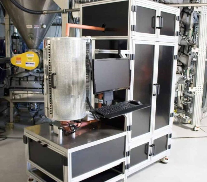
ESPOO, Finland, 2nd January 2020 (LINK) – Picosun Group, global provider of leading AGILE ALD® (Atomic Layer Deposition) thin film coating solutions, reports record performance of silicon-integrated, three-dimensional deep trench microcapacitors manufactured using its ALD technology.

Increasing efficiency and performance demands of portable and wearable electronics, along with their shrinking size in accordance with the Moore’s law, set new challenges to the power management of these devices as well. A solution is further integration of the devices’ key components into so-called SiP (systems-in-package) or SoC (systems-on-chip) architectures, where everything, including the energy storage such as batteries or capacitors, is packed close to each other into one compact, microscale-miniaturized assembly. This calls for novel techniques to increase the performance and shrink the size of the energy storage unit as well. Three-dimensional, high aspect ratio and large surface area deep trench microcapacitors where ultra-thin, alternating layers of conducting and insulating materials form the energy storing structure, provide a potential solution.


Figures above: Main technological steps of 3D microcapacitor fabrication. 1: patterning of a square lattice of holes on the silicon surface; 2: high aspect ratio trenching of silicon by electrochemical micromachining (ECM); 3: atomic layer deposition (ALD) of conformal metal-insulator-metal (MIM) stack; 4: aluminium deposition and contact patterning (*).

Picosun’s ALD technology has now realized unprecedented performance of these 3D microcapacitors. PICOSUN® ALD equipment were used to deposit film stacks of conductive TiN and insulating dielectric Al2O3 and HfAlO3 layers into high aspect ratio (up to 100) trenches etched into silicon. Up to 1 µF/mm2 areal capacitance was obtained, which is the new record for this capacitor type. Also power and energy densities, 566 W/cm2 and 1.7 µWh/cm2, were excellent and surpassing the values achieved with the most of the other capacitor technologies. The ALD microcapacitors showed also outstanding voltage and temperature stability, up to 16 V and 100 oC, over 100 hours continuous operation (*).


Figures above: b) SEM cross-section of an array of cylindrical trenches with a pitch of 4 μm, diameter of 2 μm and aspect ratio of 100, conformally coated with an ALD stack consisting of 40 nm of TiN, 40 nm of Al2O3, and 40 nm of TiN. Insets show a detail of the MIM stack at the top and bottom of a single trench; d) high-resolution TEM image of an MIM stack consisting of 40 nm of TiN, 40 nm of Al2O3, and 40 nm of TiN taken at the bottom of ALD-coated trenches with aspect ratio of 100; e) TEM-EDX elemental maps of Ti (yellow), N 14 (cyan), Al (red), and O (green) of the MIM stack in (d) (*).

These excellent performance indicators pave the way to industrial applications of this capacitor technology. This is further facilitated by ALD’s mature position in modern semiconductor industries, where the technology is already integrated into practically all advanced microchip component manufacturing lines.

“We exploited the room available on the bottom of silicon wafers, of which only a few micrometers of silicon are used for electronic components in integrated circuits, to fabricate silicon-integrated 3D microcapacitors with unprecedented areal capacitance. The electrochemical micromachining technology, developed at the University of Pisa over the past decade, enabled etching of high density trenches with aspect ratios up to 100 in silicon, a value otherwise not achievable with deep reactive ion etching. This posed the basis for increasing the areal capacitance of our 3D microcapacitors upon conformal coating with an ALD metal-insulator-metal stack,” says Prof. Giuseppe Barillaro, group leader at the Information Engineering Department of the University of Pisa, Italy.

“The suberb results achieved with our 3D silicon-integrated microcapacitors show again how imperative ALD technology is to modern microelectronics. We are happy that we can offer our unmatched expertise and decades of cumulative know-how in the field to develop novel solutions for the challenges the industry is facing, when the requirements for system performance and integration level increase inversely to the system size. The environmental aspect is also obvious, when smaller, more compact devices manufactured in the same line mean also smaller consumption of materials and energy,” says Juhana Kostamo, deputy CEO of Picosun Group.
(*) “Three-dimensional silicon-integrated capacitor with unprecedented areal capacitance for on-chip energy storage”, Lucanos M. Strambinib,1, Alessandro Paghia,1, Stefano Mariania, Anjali Soodc, Jesse Kalliomäkic, Päivi Järvinenc, Fabrizio Toiad, Mario Scuratid, Marco Morellid, Alessio Lampertie, Giuseppe Barillaroa,b,, accepted for publication in Nano Energy, https://doi.org/10.1016/j.nanoen.2019.104281.
a Dipartimento di Ingegneria dell’Informazione, Università di Pisa, via G. Caruso 16, 57122, Pisa, Italy
b Istituto di Elettronica e di Ingegneria dell’Informazione e delle Telecomunicazioni, Consiglio nazionale delle Ricerche, via G. Caruso 16, 57122, Pisa, Italy
c Picosun Oy, Tietotie 3, Espoo, FI-02150, Finland
d ST Microelectronics, via Olivetti 1, Agrate Brianza, Italy
e IMM-CNR, Unit of Agrate Brianza, Via C. Olivetti 2, 20864, Agrate Brianza, MB, Italy
(Funding from the ECSEL Joint Undertaking through the R2POWER300 project, grant no. 653933)

Wednesday, December 18, 2019

2020 CMC Conference New Session on Advanced Packaging Materials - CHIPS & EMIB for SiP


San Diego, CA, December 17: The Critical Materials Council (CMC) of semiconductor fabricators and TECHCET announce a new addition to the 2020 CMC Conference

Advanced Packaging Materials. Scheduled for April 23-24 in Hillsboro, Oregon, the 5th CMC Conference, will explore actionable technical and value-chain trends of critical materials for global semiconductor fabs and feature keynotes from leaders in semiconductor technology and materials. The conference keynote address this year will be:

"Critical Materials Pushing the Limits for Semiconductor Manufacturing"
by Bruce Tufts, Vice President of Technology and Director of Fab Materials Organization, Intel Corp.

Sessions will cover: 
I. Global Value-chain Issues, Including Economics and Regulations,
II. Immediate Challenges of Materials & Manufacturing,
III. Emerging Materials in R&D and Pilot Fabrication, and
  New this year is a fourth session,
IV. Advanced Packaging Materials

Lead by Session Chairman Jim Hannah, Product Development and Applications Manager of SEH, the Advanced Packaging Materials Session will address, system level performance scaling issues and the increased reliance on packaging. As explained by Mr. Hannah, “We see the lines starting to blur between packaging and the back-end wiring on-chip. The CMC Conference will cover both current challenges and future requirements of packaging materials needed to support this middle-ground."

A keynote address on “The Future of Silicon as a Packaging Material" for this new session will be provided by Dr. Subramanian Iyer, principle of UCLA’s Center for Heterogeneous Integration and Performance Scaling (CHIPS) consortium, IEEE Fellow, IBM Fellow, IIT Distinguished Alumnus, and UCLA Distinguished Chancellor's Professor of both Electrical and Computer Engineering and Materials Science and Engineering.


Dr. Lauren Link, Intel's Technical Program Manager, Substrate Business Group, will present on materials to enable Embedded Multi-die Interconnect Bridge (EMIB) connections between silicon chiplets in advanced Heterogeneous Integration (HI) System-in-Package (SiP) products.

CMC member companies will be attending the public CMC Conference, which follows the annual members-only CMC meeting to be sponsored by Intel and held April 21-22. Conference attendees will include industry experts handling supply-chains, business-development, R&D, and product management, as well as academics and analysts. Business drives our world, but technology enables the profitable manufacturing of semiconductor devices and facilitates the introduction of new materials.

To submit a paper for consideration, send a 1-page abstract focusing on critical materials supply dynamics by January 15, 2020 to

For more information and registration:


 For more information on CMCFabs or CMC Associate Memberships, please contact Diane Scott at dscott@techcet.com. For information on sponsoring the CMC Conference please contact Yvonne Brown at ybrown@techcet.com, +1-480-382-8336 x1.

CMC Fab members include:


Copyright 2019 TECHCET CA LLC all rights reserved