Thursday, January 10, 2019

Semiconductor Materials Market will be +3% to $50.4B in 2019

TECHCET-the electronic materials advisory services firm providing business and 
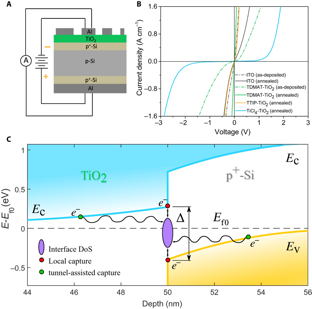
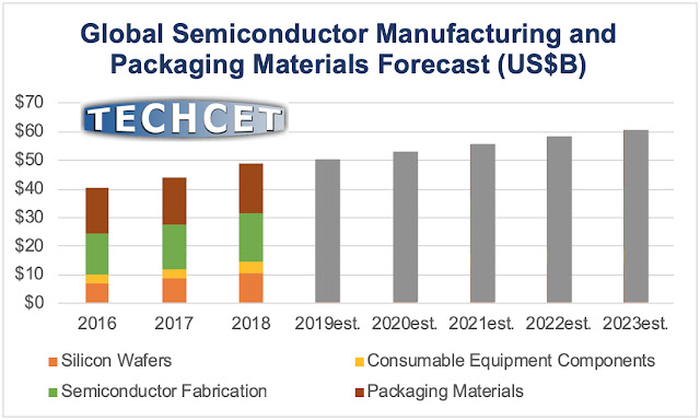
technology information- announced that global revenues for semiconductor manufacturing and packaging materials are expected to grow 3.1% year-over-year (YoY) in 2019 to US$50.4B, of which 58% represents semiconductor fab materials. Steadily increasing demand for memory chips in 2018 lifted total materials market revenues to US$48.9B in 2018, while the compound annual growth rate (CAGR) through 2023 is forecast at 4.3% as detailed in the latest TECHCET Critical Materials Reports (CMR) and shown in the attached figure.


Global trade issues in 2018 run the risk of devolving into real trade wars, if governments and companies do not negotiate business terms from a place a mutual respect. "Wars can only have winners and losers," reminded Lita Shon-Roy, TECHCET President and CEO. "While issues can have win-win resolutions after mutually-respectful negotiations." 


At the 2018 Critical Materials Council (CMC) Seminar, held last October in Ningbo, China in coordination with China's IC Materials Technology Innovation Alliance (ICMtia), representatives of global chip-makers including Intel, GlobalFoundries, and Texas Instruments discussed ways to ensure electronic materials supply-chain robustness in an era of short-sighted protectionist tariffs. All three companies have high-volume manufacturing (HVM) fabs in mainland China along with the US, and all need to source a wide range of specialty materials from global suppliers.

During private face-to-face meetings between CMC fab members in Ningbo, held just after the public CMC Seminar, ON Semiconductor shared that they have a plan prepared to deal with tariffs goings into effect at different levels. Established HVM chip fabs must keep sourcing specialty materials regardless of political whims, because our modern world relies on a steady supply of semiconductor devices to maintain our communications, entertainment, health-care, and transportation infrastructures.

Critical Materials Reports™ and Market Briefings: https://techcet.com/shop/

ABOUT TECHCET: TECHCET CA LLC is an advisory services firm focused on process materials supply-chains, electronic materials business, and materials market analysis for the semiconductor, display, solar/PV, and LED industries. Since 2000, the company has been responsible for producing the SEMATECH Critical Material Reports™, covering silicon wafers, semiconductor gases, wet chemicals, CMP consumables, Photoresists, and ALD/CVD Precursors. The Critical Materials Council (CMC) of semiconductor fabricators is a business unit of TECHCET, and includes materials supplier Associate Members. For additional information about reports, market briefings, CMC membership, or custom consulting please contact info(at)cmcfabs.org, +1-480-332-8336, or go to http://www.techcet.com or http://www.cmcfabs.org.

Call for Abstracts - AVS ALD 2019 and ALE 2019!


Call for Abstracts
Deadline February 15, 2019

The AVS 19th International Conference on Atomic Layer Deposition (ALD 2019) featuring the 6th International Atomic Layer Etching Workshop (ALE 2019) will be a three-day meeting dedicated to the science and technology of atomic layer controlled deposition of thin films and now topics related to atomic layer etching. The conference will take place Sunday, July 21-Wednesday, July 24, 2019, at the Hyatt Regency Bellevue in Bellevue, Washington (East Seattle).

As in past conferences, the meeting will be preceded (Sunday, July 21) by one day of tutorials and a welcome reception. Sessions will take place (Monday-Wednesday, July 22-24) along with an industry tradeshow. All presentations will be audio-recorded and provided to attendees following the conference (posters will be included as PDFs). Anticipated attendance is 800+.


Key Deadlines:
Abstract Submission Deadline: February 15, 2019
Author Acceptance Notifications: April 8, 2019
Early Registration Deadline: June 1, 2019
Hotel Reservation Deadline: June 27, 2019
JVST Special Issue Deadline: November 1, 2019


ALD Program Chairs

Program Chair:
Sumit Agarwal
(Colorado School of Mines, USA)

Program Co-Chair:
Dennis Hausmann
(Lam Research, USA)
ALE Program Chairs

Program Chair:
Craig Huffman
(Micron, USA)

Program Co-Chair:
Gottlieb Oehrlein
(University of Maryland, USA)


Wednesday, January 9, 2019

Australian-Californian team present ALD TiO2 for high-efficiency monolithic perovskite/Si tandem cells

Here is quite promising results on fabricating ALD  TiO2 high-efficiency monolithic perovskite/Si tandem cells in a joint collaboration between California Institute of Technology, USA, and The Australian National University, Canberra, and Flinders University, Adelaide,in Australia.

In situ recombination junction between p-Si and TiO2 enables high-efficiency monolithic perovskite/Si tandem cells

Heping Shen, Stefan T. Omelchenko, Daniel A. Jacobs, Sisir Yalamanchili, Yimao Wan, Di Yan, Pheng Phang, The Duong, Yiliang Wu, Yanting Yin, Christian Samundsett, Jun Peng, Nandi Wu, Thomas P. White, Gunther G. Andersson, Nathan S. Lewis and Kylie R. Catchpole

Science Advances 14 Dec 2018: Vol. 4, no. 12, eaau9711, DOI: 10.1126/sciadv.aau9711 

Distributed under a Creative Commons Attribution NonCommercial License 4.0 (CC BY-NC).

[Abstract] Increasing the power conversion efficiency of silicon (Si) photovoltaics is a key enabler for continued reductions in the cost of solar electricity. Here, we describe a two-terminal perovskite/Si tandem design that increases the Si cell’s output in the simplest possible manner: by placing a perovskite cell directly on top of the Si bottom cell. The advantageous omission of a conventional interlayer eliminates both optical losses and processing steps and is enabled by the low contact resistivity attainable between n-type TiO2 and Si, established here using atomic layer deposition. We fabricated proof-of-concept perovskite/Si tandems on both homojunction and passivating contact heterojunction Si cells to demonstrate the broad applicability of the interlayer-free concept. Stabilized efficiencies of 22.9 and 24.1% were obtained for the homojunction and passivating contact heterojunction tandems, respectively, which could be readily improved by reducing optical losses elsewhere in the device. This work highlights the potential of emerging perovskite photovoltaics to enable low-cost, high-efficiency tandem devices through straightforward integration with commercially relevant Si solar cells.

Schematic illustration and morphological characterizations of the interlayer-free monolithic perovskite/Si tandem solar cell : (A) Schematic of the interlayer-free monolithic perovskite/crystalline-silicon (c-Si) tandem solar cell (not to scale). Initial tests were carried out on homojunction Si cells with Spiro-OMeTAD (Spiro) as the top perovskite contact; however, our best performance was obtained with polysilicon (poly-Si) bottom cells and PTAA {poly[bis(4-phenyl)(2,4,6-trimethylphenyl)amine]} as the top hole-selective layer. (B) Cross-sectional SEM image of the tandem device based on a Si homojunction subcell from the top surface to the p+-Si layer [Spiro-OMeTAD is used as a hole transport material (HTM)]. The antireflection layer was not included because of the large thickness of ~1 mm. (C) Scanning transmission electron microscopy (STEM) bright-field (BF) image, and (D) high-resolution STEM BF image of the TiO2/p+-Si interface.

The TiO2 layers prepared using different ALD precursors and ALD systems yielded markedly mutually different J-V characteristics in our TiO2/p+-Si test structures (below). 
  • Ohmic, highly conductive behavior between TiO2 and p+-Si was observed in samples with TiO2 prepared using tetrakisdimethylamidotitanium (TDMAT) as the ALD precursor (green solid line)
  • Very low conductivity (ρ > 10 ohm·cm2) in the low-bias region was obtained when using titanium tetrachloride (TiCl4) instead (blue solid line) 
  • Titanium tetraisopropoxide (TTIP) resulted in intermediate performance, displaying conductive but distinctly nonlinear J-V behavior (yellow solid line).
The ALD processing was conducted in two different ALD reactors:
  • TDMAT process : Ultratech Fiji 200 Plasma ALD system (now Veeco CNT)
  • TiCl4 process : BENEQ TFS200
  • TTIP process : BENEQ TFS200

Contact behavior and simulated band diagram of TiO2/p+-Si interfaces. (A) Schematic of the structure used for measuring contact resistivity. (B) Comparison of the J-V behavior of ITO/p+-Si and various TiO2/p+-Si structures before and after annealing at 400°C in air. TiCl4-ALD TiO2 listed here is deposited with a reactor chamber temperature of 75°C. (C) Simulated band diagram of the TiO2/p+-Si at equilibrium assuming n-type doping of 5 × 1018 cm−3 on TiO2 and 1019 cm−3 for p+-Si (appropriate for our test structure with TDMAT TiO2; see table S3). The unknown interfacial energy gap Δ is shown here for illustrative purposes as 600 meV, which falls within the range of reported measurements (31). Both mechanisms of direct- and tunneling-assisted capture by interfacial density of states (DoS) are shown.

The Australian-Californian team conclude :
  • Successful demonstration of two proof-of-concept 2-T perovskite/Si tandem devices that function without a conventional interlayer between their subcells.
  • fabrication of an nc-Si tunnel junction interconnect is relatively straightforward for HIT cells, these layers introduce a small but potentially important amount of parasitic loss in the region of ~550 to 700 nm (16), where the nc-Si is absorbing and the perovskite top cell’s absorption is simultaneously incomplete.
  • The publication of a similar scheme using SnO2 (40) instead of TiO2 while this paper was under review demonstrates the wide applicability of the interlayer-free concept. Jointly, our work highlights the potential of emerging perovskite photovoltaics to enable low-cost, high-efficiency tandem devices through straightforward integration with commercially relevant and emerging Si solar cells.

Tuesday, January 8, 2019

Review form IEDM2018 - The World After Copper

Here is a very good review form IEDM2018 - The World After Copper by Paul McLellan

Thank you for sharing this one Henrik Pedersen! Indeed, Ru is coming!

IEDM: The World After Copper

I remember Gary Patton, the CTO of GLOBALFOUNDRIES, telling me once that research seemed to have flipped, and whereas he used to have most people working on transistors and interconnect was an afterthought, now it was the other way around. Just scaling the existing copper interconnect to get to the next generation was no longer enough.

At IEDM in December, there was a special session called Interconnects to Enable Continued Scaling. There were invited presentations by:
  • Arm and Georgia Tech
  • IBM
  • imec
  • UT Austin and GLOBALFOUNDRIES
  • Stanford
  • Applied Materials
Continue reading LINK 

LG Display’s 65-inch rollable OLED TV will go to production

ALD moisture barriers for flexible and shaped electronics, displays and solar cells have been researched, developed and scaled up for production for some time now. Besides rounded display edges of smart phones and gizmo's that have been shown at trade shows and other events there has not yet been that many potential high volume markets out there.
 
 
LG Display’s 65-inch rollable OLED TV as presented at CES2019 (youtube.com)
 
It’s been a year since LG Display’s 65-inch rollable TV prototype was demonstrated at CES, and now LG Electronics is bringing it to market as the company’s flagship 4K OLED TV for 2019. The finished Signature OLED TV R that consumers will be able to buy sometime this spring — for an astronomical, premium price — is quite similar to that prototype, but LG has refined the base station and added a 100-watt Dolby Atmos speaker for powerful built-in audio.This is a TV that’s there when you want it and disappears when you don’t. 
 
 
Youtube: LG Display’s 65-inch rollable OLED TV is only a prototype, so there’s no price or release date, but it’s still very cool. The Verge Senior editor Vlad Savov got a first look at the TV at CES 2018.
 
Not everyone loves having a big, black rectangle as the focal point of their living room, and plenty of people don’t own a TV at all. This TV disappears completely whenever you’re not watching. It drops slowly and very steadily into the base and, with the push of a button, will rise back up in 10 seconds or so. It all happens rather quietly, too.There’s also a mode — LG calls it “Line Mode” — where the display will drop down so that only about one-fourth of the panel is showing. You’ll still have on-screen music controls and the option to control your smart home gadgets in this mode. 
 
LG also includes some mood-setters like a crackling fireplace or rain sounds. Support for Alexa voice controls are being added this year in addition to the existing Google Assistant integration in LG’s webOS software; you just hold down the Prime Video button on the remote to bring up Alexa. And LG is also one of the companies that’s adding Apple’s AirPlay 2 for easy media playback or device mirroring. You can play music on the Atmos speaker system even when the TV is fully rolled up, which is great. Port selection is on par with other premium LG sets, and they’re all located at the back of the base. LG is making the move to HDMI 2.1 with its 2019 series, so that’s a big plus in terms of future proofing this very expensive TV.

Source: The Verge (LINK)

---------------------
By Abhishekkumar Thakur and Jonas Sundqvist

Monday, January 7, 2019

Picosun to showcase ALD for Medical applications at MDM West

ALD is steaming ahead into new fields and applications boyond the semiconductro industry. Meet Picosun at MDM West, the largest medtech event in North Americ.


Related Blog posts:

Nanexas PharmaShell® patent approved in the United States
Nanexa order a third Picosun ALD System to meet production demand for PharmaShell®
Picosun’s ALD nanolaminates extend the lifetime of biomedical microimplants
Picosun launches new PicoMEDICAL™ solutions specially targeted for healthcare industries
Groundbreaking micromedicine with Picosun’s ALD solutions

Versum Materials report 1,000 CHEMGUARD® GEN III Systems sold

[Versum Materials Newsletter, LINK] An important milestone for the Versum Materials DS&S was realized recently with the sale and commissioning of the onethousandth (1,000) CHEMGUARD® Gen III high-purity, liquid delivery system since its introduction in 2016. The 1,000-plus units are now running in the latest high-volume semiconductor fabs globally with more than 200 molecules now approved for delivery. Built on a legacy of more than 30 years of supplying advanced materials and delivery systems to the worldwide semiconductor and electronics industries, Versum Material’s DS&S team continues to design and build safer, more reliable delivery equipment for high-purity gas and liquid distribution.
 
 
CHEMGUARD 500 is specifically designed for very low vapor pressure precursors. The patented, automa􀆟c solvent purge ensures molecule purity on some of the lowest vapor pressure molecules used in semiconductor manufacturing. A small sample of the molecules approved in a CG500 are: TDMAT, TDEAT, TAETO, TBTDET, TDEAH, TEMAH, TEMAHf, TEMAZr and TPOSL. (From the CHEMGUARD GEN III 500 DATA SHEET)

“The CHEMGUARD Gen III system has been very well received by Versum Materials major customers, especially with its built-in redundancies,” said Jeff Chung, DS&S Asia Sales Manager.

Said David Eshelman, CHEMGUARD Product Manager, “The CHEMGUARD product family was introduced in 1999 under the Schumacher brand. Our customers’ original requests for improved safety and uptime helped to create the CHEMGUARD systems.”

Eshelman further explained that those requirements still exist today, but with each node, the molecules and processes used have become much more technically challenging. “The specific needs of today’s specialty, flammable or highly energetic molecules have been addressed by the unique CHEMGUARD Gen III model designs.”

Capitalizing on its materials and delivery systems expertise, Versum Materials recently created an experienced, multidisciplined team to review new molecules as they ramp and gain market acceptance. The team evaluates the molecule safety and process needs and helps speed the time-to-market for new molecules and processes by having a delivery solution ready when technology ramps.

“When our team says ‘Go,’ we know that a molecule is CHEMGUARD-ready,” said Eshelman. “The next node is right around the corner. We want the market to know that the established CHEMGUARD system continues to advance to meet the demands of a changing marketplace.”

CHEMGUARD GEN III CONTROLLER RETROFIT DATA SHEET (http://bit.ly/2PO164F)
CHEMGUARD GEN III 500 DATA SHEET (http://bit.ly/2zlnFU8)
CHEMGUARD GEN III 100 – 400 DATA SHEET (http://bit.ly/2QhjOBd)

Saturday, January 5, 2019

EuroCVD 22 & Baltic ALD 16 | 24-28 June 2019, Luxembourg Abstract submission deadline: 21 January 2019

The EuroCVD 22-Baltic ALD 16 Conference will take place in Luxembourg on 24-28 June 2019. The conference will offer a high quality scientific program with invited and contributed lectures in key development areas based on chemical processing from the gas phase.


The submission of contributions is open up to the 21st of January 2019.

Submit your abstract

Friday, January 4, 2019

Nanexas PharmaShell® patent approved in the United States

The US Patent Office has approved Nanexa's patent application for the PharmaShell® drug delivery platform.

Nanexa AB is a nanotechnology drug delivery company focusing on the development of PharmaShell®, which is a new and groundbreaking drug delivery system that is expected to have great potential in a number of medical indications. Within the framework of PharmaShell®, Nanexa has partnership agreements with among others, AstraZeneca.

The US Patent Office has approved Nanexa's patent application on January 1, 2019. The now-approved patent covers the product PharmaShell® as well as the method of its manufacture and formulation of PharmaShell® coated drugs. The approved patent has patent number US 10166198.

CEO David Westberg comments:

It is with great satisfaction that I can now conclude that the PharmaShell® patent is approved in the United States. We have always felt secure in our patent situation, but it still means a lot to get it confirmed by the US Patent Office. The US is our largest market and now that we have an approved patent, we can have a more interesting position in discussions with potential partners.

Source : Nanexa (in Swedish, LINK)

Nanexa order a third Picosun ALD System to meet production demand for PharmaShell®

[Picosun, LINK] ESPOO, Finland, 4th January 2019 – Picosun Group, a leading, global supplier of ALD (Atomic Layer Deposition) thin film coating technology, and Nanexa AB, a nanotechnology company focused on nano-enabled drug delivery solutions, solidify their collaboration in pharmaceutical ALD.


Picosun is now delivering their third ALD system to Nanexa’s facilities in Sweden, where it will be utilized in production expansion of nano-functionalized pharmaceuticals for drug delivery. Stock-listed Nanexa AB has two patents pending for their technology platform PharmaShell®. With this technology, ALD-functionalized pharmaceuticals can stay effective in the body for long periods of time and have a tailored release profile that minimizes side effects and eliminates the need for constant re-dosing. Picosun has been aiding Nanexa in their undertaking to develop their technology to an industrially mature state by supplying ALD tool solutions and consultancy.

Picosun provides various ALD solutions specially optimized to meet the needs of the medical industries where quality, reliability, efficiency, patient safety and minimized side effects are of utmost importance.

“We are very pleased to order our third PICOSUN™ ALD system. We have reached a point where the demand from our commercial partner to invest in our technology platform PharmaShell® is rapidly increasing. To be able to meet this demand we are now procuring a new ALD tool to extend our production capacity for efficient delivery of materials to our customers,” says David Westberg, CEO of Nanexa.

“We are happy to provide yet more PICOSUN™ ALD equipment to our long-time partner Nanexa, where our technology is used in manufacturing state-of-the-art medicines to combat some of the most difficult diseases. Our aim is to utilize ALD to enable solutions that benefit the whole humanity, which is why we are especially glad that healthcare industries are now seizing the potential of ALD on so many fronts,” continues Dr. Jani Kivioja, CTO of Picosun.

Thursday, January 3, 2019

Innovation and IP filing in Atomic Layer Deposition has moved from Memory to Logic

By studying the filing of IP world wide one can clearly see the trend how innovation in Atomic Layer Deposition (ALD) has moved from Memory to Logic. During the introduction of ALD (2003 to 2006) in high volume manufacturing of DRAM on 300 mm wafers most IP was filed by Samsung, Micron and SK Hynix. 10 years later (2013-2018) the IP filing lead has been taken over by Logic MPU manufacturers TSMC, Intel and Globalfoundries.

The patent application assignee from the past 25 years.

ASM International received a supplier excellence award from TSMC

[ASM International, LINK] ASM International N.V. (Euronext Amsterdam: ASM) has received a supplier excellence award as one of five equipment suppliers from TSMC for the performance and support of ASM's CVD equipment and technology during 2018. The award was presented to ASM by Dr. C.C. Wei, TSMC's Chief Executive Officer, at the TSMC Supply Chain Management Forum on December 6, 2018 in Taiwan.

The award was received by ASM in recognition of its CVD technology and performance in production at TSMC fabs. During the presentation, TSMC explained three points that contributed to the award to ASM.

1) Close engagement with TSMC and precursor suppliers to innovate process solutions.

2) Continued effort on cost and productivity improvement.

3) Exceptional manpower arrangement for delivery.


"We are very honored to receive this prestigious award from TSMC. On behalf of ASM, I would like to thank TSMC for this recognition," said Chuck del Prado, CEO and President of ASM International. "ASM strives to continuously advance our technology solutions and our partnership with TSMC is of strategic importance to ASM. We are very pleased that TSMC has benefited from the performance of our ALD and Epitaxy deposition tools in its production fabs."

TSMC is the world's largest semiconductor manufacturing foundry. TSMC holds the Supply Chain Management Forum annually to show appreciation for the support and contributions of their suppliers and to recognize outstanding equipment and materials suppliers.

Call Abstracts - Nano-Optics International School Feb 2019

Nano-Optics International School. Feb 2019. Call Abstracts. Early Bird Registration.

Venue: International Iberian Nanotechnology Laboratory (INL),Braga, Portugal

http://nano-optics-school-2019.org/


The 2nd Edition of IUVSTA NANO OPTICS School ha been organized to provide the rare opportunity to learn from and interact with some of the top experts in the field, both from academia and from companies. Ph.D. and master students are encouraged to attend the School and present their research work. Strong interaction between lecturers and students will be promoted during the entire school. Sessions on “Science Communication” and on “Project Management” oriented for students and young researchers are included in the programme. A guided visit to the INL laboratory http://inl.int/ is included in the programme.

COST Action MP1402 - HERALD
Hooking together European research in Atomic Layer Deposition

Wednesday, January 2, 2019

IEDM 2018 Imec on Interconnect Metals Beyond Copper

At IEDM in December 2018 Imec presented recent results from their interconnect program “Interconnect metals beyond copper – reliability challenges and opportunities”, which was recently covered by Scotten Jones (SemiWiki).
 

The electrical current in interconnect lines haven’t scaled down as fast as the lines' cross sectional area, which has enhanced the current density in the lines. Initial wide aluminum (Al) interconnects were first replaced by narrower aluminum-copper (AlCu) alloys and eventually by Cu to reduce the interconnects line resistance. Now even Cu needs to be replaced by alternate materials for the narrowest lines due to the following limits:

  • Higher resistivity with shrinking line width – below 20nm exponential increase in line resistance.
  • Via resistance also goes up strongly due to the liner.
  • Thinner lines see more grains from electroplating – around 10nm line can’t meet electromigration.
Imec commenced their work on alternative materials for M0 and M1 interconnects by screening based on the two metrics—resistivity multiplied by electron mean free path and melting point. The work reflects Rhodium and Iridium as the best candidate materials for the lowest interconnects that can be reasonably integrated. Ruthenium (Ru) and Cobalt (Co) exhibit similar performance. These materials can be deposited using ALD, CVD or electroplating. Co needs a thin adhesion layer but not a barrier layer. Ru also doesn’t require any seed or barrier layer. Imec is still working on reliability tests of these materials.

Meanwhile, TSMC has been using Co capping on Cu interconnects since 16 nm due to improved electromigration. Co (TSMC) and Ru (Intel) seed layers were introduced. Intel has introduced Co contacts at 10 nm and TSMC at 7 nm. Intel has also introduced Co interconnects for metals 0 and 1 at 10 nm.

Source: SemiWiki, Scotten Jones : LINK
 
----------
By Abhishekkumar Thakur