Friday, November 9, 2018

Coverage, Composition and Band Gap Analysis of ALD-Grown Ultra Thin Films

[AZO Network News E-mail] Analyzing and developing ultra-thin film materials requires multiple data points typically from multiple instruments and techniques. Find out how one surface analysis instrument provides a complete picture of an ALD-grown ultra-thin film with information on composition and thickness, surface coverage and band gap measurements.


The Thermo Scientific™ Nexsa XPS System is not only a fully automated and intuitively programmed device, but has the advantage of being able to offer multi-technique analysis as well. This has made it a still more efficient and useful machine than its predecessor, the highly successful Thermo Scientific™ K-Alpha XPS system.

The Nexsa makes coincident analysis possible because it uses multiple methods, namely, UV photoelectron spectroscopy (UPS), ion scattering spectroscopy (ISS), reflected energy loss spectroscopy (REELS) and Raman spectroscopy. Taking advantage of this capability, the Nexsa was used to investigate various properties of a set of samples of HfO2. Each sample was made up of a thin layer of HfO2 laid down using a graded number of atomic layer deposition (ALD) cycles. Initially, the mass of Hf laid down on the substrate was measured quantitatively using XPS, as well as the thickness of the layers of HfO2 and SiO2. ISS and REELS were then used to carry out further analysis to obtain surface coverage and band gap readings respectively.

Full article : LINK

Introductory lecture on ALD available as "Panopto" lecture capture, and slides in SlideShare

Introductory lecture on ALD available as "Panopto" lecture capture, and slides in SlideShare by Prof. Riikka Puurunen, Aalto University, Finland.

SlideShare : LINK

Panopto Open Teaching Video : LINK

RASIRC : Effective Silicon and Metal Nitride Deposition at Reduced Temperature

[RASIRC Technical Brief] Silicon and metal nitrides are extensively used in the semiconductor industry in logic and memory chip manufacturing. PEALD approaches have found success in this area but carry significant risk of poor step coverage and surface damage in 3D and HAR structures. When non-line-of-sight deposition is required, thermal ALD is the preferred solution along with co-reactants that can deposit high quality films at temperatures below 430°C.
Source: RASIRC Technical Brief (LINK)

Imec to present Highest-Density 3DS Stacked FinFETs at IEDM 2018

Here is an interesting paper to be presented by Imec at the upcoming IEDM 2018 in San Fransisco. Imec has managed to stack the complete FinFET front end module on top of a "standard" bulk silicon FinFET Module demonstrating also good threshold voltage tuning, reliability and low-temperature performance. 

So just imagine if this would be used in high volume manufacturing - it would mean that all those ALD processes used in patterning and for the high-k metal gate module, spacers, local interconnect etc. etc. would come twice meaning a 2X need for ALD process chambers. And lets say you can run this twice - is there any reasons why you can´t run it yet another time? Woah!

Also as a note, Imec is here using a LaSiOx layer an a dipole inserted in the HKMG stack - presumably it is an ALD process since it will have to conformally coat this fins and ensure precise thickness control and uniformity.

So just enjoy seeing double - it is Friday!

Paper #7.1, “First Demonstration of 3D Stacked FinFETs at a 45nm Fin Pitch and 110nm Gate Pitch Technology on 300mm Wafers,” A. Vandooren et al, Imec

Highest-Density 3DS Stacked FinFETs: Imec researchers will report on 3D stacked FinFETs that have the tightest pitches ever reported in such a stacked architecture – 45nm fin pitch and 110nm gate pitch. The 3D architecture makes use of a sequential integration process yielding tight alignment between very thin top and bottom Si layers. The junction-less devices in the top layer were fabricated and transferred using low-temperature (≤525ºC) processes to avoid performance degradation, and a 170nm dielectric was used to bond the two wafers. The top layer is so thin that the bottom layer could be patterned right through it by means of 193nm immersion lithography, which connects the two via local interconnect. The researchers evaluated various gate stacks, ultimately choosing TiN/TiAl/TiN/HfO2 with a LaSiOx dipole inserted into the stack. The combination demonstrated good threshold voltage tuning, reliability and low-temperature performance.

At left above is a cross-sectional electron microscope image of the fabricated 3D stacked FinFETs along fins and across gates, showing the tight alignment achieved by the top processed layers (Gate Li1, Li2) toward the bottom layers. At right is a cross-sectional image of the final devices across fins with the gates covering the fins.


“First Demonstration of 3D Stacked FinFETs at a 45nm Fin Pitch and 110nm Gate Pitch Technology on 300mm Wafers,” A. Vandooren et al, Imec (IEDM 2018 Press kit)

Source: IEDM Press kit (LINK)

Tuesday, November 6, 2018

Beneq to present new automated wafer batch ALD platform at Semicon Europa

Beneq is presenting their new automated wafer batch ALD platform Beneq C2 at Semicon Europa in Munich November 13 to 16, 2108.

[From Beneq News Letter] Come and visit us in Semicon Europa and hear all about the latest version of our award-winning Beneq C2 automated wafer batch ALD platform with a special focus on emerging ALD markets, such as moisture barriers, passivation, insulators, anti-corrosion coatings for Power Si & WBG, RF GaAs, GaN and Si, MEMS sensors and actuators, Image sensors, LED and OLED.

Book a meeting with the Beneq team in Semicon Europa
 

La 4ème édition du colloque RAFALD aura lieu du mardi 6 au jeudi 8 novembre 2018 à Lyon.

La 4ème édition du colloque RAFALD aura lieu du mardi 6 au jeudi 8 novembre 2018 à Lyon.

1ère édition de l'école d'automne de l'ALD le mardi 6 novembre matin

Ce workshop dédié à la technologie ALD (Dépôt de Couches Atomiques - Atomic Layer Deposition) a pour but de fédérer une communauté française (industrielle et académique) pour initier la création d’un réseau national.

Pour cela nous organisons un colloque annuel réunissant tous les acteurs français actuels de l'ALD (universitaires et industriels) et également les techniciens, ingénieurs, doctorants, chercheurs et enseignants chercheurs potentiellement intéressés par l'ALD.

Ce colloque regroupe à la fois des sessions de formation et également des exposés scientifiques oraux et par affiches.
Public visé : Laboratoires académiques, industriels
Domaines visés : microélectronique, énergie, textile, biologie, nanotechnologies.
Niveau : Tous niveaux.

La LINK


Review Article - ALD for oxide semiconductor thin film transistors

Review Article: Atomic layer deposition for oxide semiconductor thin film transistors: Advances in research and development

Jiazhen Sheng, Jung-Hoon Lee, Wan-Ho Choi, TaeHyun Hong, MinJung Kim, and Jin-Seong Park
Journal of Vacuum Science & Technology A 36, 060801 (2018)


Sunday, November 4, 2018

Foundry investment in 5nm has started according to ASM

Here are some take aways form the ASM International Earnings Call for Q3/2018 [Full transcript by Seeking Alpa, LINK]. Interestingly there was no talk about "The end of Moore´s Law" at all. On the contrary ASM see that Foundry investment in 5nm has started and will increase in 2019 and incearsed number of additional new ALD applications will be deployed.

For ASM the equipment sales were led by their ALD business, but they also recorded healthy sales levels in our other product lines. By industry segment, revenue in the quarter was led by foundry, followed by memory and then logic. Within memory the larger part of sales was related to DRAM investments, while NAND sales decreased compared to the second quarter. 
 
"The structural outlook for the ALD market remains strong. ALD continues to be a key enabler of Moore's Law. An increasing number of ALD steps will be needed to help create the smaller geometries, new materials, and more complex device architectures that are on our customers' roadmap." 
 
- Chuck del Prado, President and CEO of ASMI.
  • Spending in the advanced logic segment is clearly higher in 2018 compared to last year.
  • Foundry spending is lower this year and is driven by further 7-nanometer investments as well as the first investments in 5-nanometer. 
  • Investments for the 5-nanometer node are likely to further increase in the course of next year.
  • ASM expectation is that the 5-nanometer foundry node is going to be an important transition for the company, with good opportunities to expand with multiple new ALD applications/layers. 
  • The DRAM segment is to show solid growth for the wafer equipment market in in 2018. For ASM, DRAM is also one of the drivers behind higher sales this year. ASM remain strongly focused on broadening our position in DRAM to new ALD solutions.
  • 3D NAND spending is coming down significantly in the second half of this year. Also, for the full year of 2018 NAND spending is expected to be lower.
  • A recovery in investments in the NAND segment will likely be driven by the transition to the next device generations of 90-plus layers. These next device generations are expected to need an increased number of advanced single wafer ALD applications.

LIST invites you to the EuroCVD 22 – Baltic ALD 16 | 2019 conference in Luxembourg on 24-28 June 2019

AP Systems to supply Thin Film Encapsulation to Samsung Display QD-OLED line

DIGITimes China reports [LINK] that Samsung Display is building a large-scale quantum dot organic light-emitting diode (QD-OLED) panel pilot production line. The line is scheduled to be finished in December 2018 and will be activated after 6 months (mid 2019). According to the report the supply ration from Korean equipment manufacturers has increased significantly for this line.

As an example the the report claims that AP Systems beat Applied Materials to supply the Thin Film Encapsulation (TFE) equipment. AP Systems has previously supplied TFE equipment for the 8th generation RGB OLED TV panel production line (V1) of Samsung Display. In the past Samsung Display has used TFE equipment supplied by Applied Materials in the 6th generation flexible OLED production line, but has now switched and for its AP Systems in this 8th generation QD-OLED test production line.

Also according to the report, the PECVD equipment will be supplied by Wonik IPS from Korea whereas the blue OLED material evaporation equipment will be supplied by Canon Tokki (Japan) and the red and green QD material inkjet printing machine will come from Kateeva (USA).
The KORONA™ TFE System running PEALD with "Multi-linear Nozzle" technology and ICP antenna design technology (high density/low damage plasma).
For TFE AP Systems are using a Plasma enhanced Atomic Layer Deposition (PEALD) technology on their KORONA™ TFE System. The system is capable of depositing a film structure that acts as a sealant to prevent oxygen and moisture penetration into OLED device. Based on a 1000Å, SiNx/SiOx multi-layer structure the Water Vapor Permeability is less than 5e-5 g/m2/day.
According to AP Systems they can also apply the film as a flexible sealant to realize flexible, rollable, and foldable displays. 


Thursday, November 1, 2018

Welcome To The World's First Open ALD Blog Platform: BALD Engineering Guest Blog

Are you willing to get recognition and attention in the ALD community? Do you hold ALD news, articles, presentations, podcasts, videos, conference/workshop/tutorial invitation or promotion in your pocket that you want to share with the ALD community?


Then, here is the world's best ALD platform: BALD Engineering Guest Blog. No matter at what stage you are in your career; this is for you if ALD or ALE is your cup of tea. Write your own blog and share your own content or interesting news on the BALD Engineering Guest Blog; also, feel free to promote it in your social media network.

Content Guidelines:

- Up to 1000 words, including html-links.
- Up to 3 images (without copyright violation).
- References as links or as DOI number for journal references.
Keep the most relevant and attention grabbing image at first as it will be the thumbnail picture for your post while sharing in your social media platforms (LinkedIn, Twitter).

Blog ending includes:

--------------------------------------
Guest blog by [first name] [last name], [affiliation] (optional)
Location: [city], [country]
Web page: (optional)
LinkedIn link: (optional)
Twitter link: (optional)

You can also submit:

Videos through YouTube stream or Twitter tweet or LinkedIn embedded feeds.

How to Submit:

Click on jonas.sundqvist@baldengineering.com to directly write or copy+paste the content or attach content file (up to 10 MB in size).

Feedback:

This is the first version of the open guest blog. Therefore, we are constantly looking forward to get feedback and suggestions to make it even handier for the users and to widespread it further. Please write your comments to us on feedback@baldengineering.com or through any social media.


Wednesday, October 31, 2018

JVSTA Call for Paper - Atomic Layer Deposition and Atomic Layer Etching

Manuscript Deadline: November 1, 2018

This special topic collection is planned in collaboration with ALD 2018 and the ALE 2018 Workshop to be held in Incheon, South Korea during July 29—August 1, 2018. The Special Topic Collection will feature sections dedicated to the science and technology of atomic layer controlled deposition and to the science and technology of controlled etching of thin films. While a significant number of articles will be based on material presented at ALD 2018 and the ALE 2018 Workshop, research articles on ALD and ALE but not presented at this conference are also welcome. The special topic collection will be open to all articles on the science and technology of ALD and ALE.


Authors are encouraged to use the JVST templates. Online, you will have an opportunity to tell us that your paper is a part of the Special Topic Collection by choosing either the “ALD Special Topic Collection” or the “ALE Special Topic Collection.”

Tuesday, October 30, 2018

Estimating rising demand for Ru thin-films in the next generation chips

STREM Chemicals offers one of the most promising ruthenium amidinate precursors for growing Ru ALD or CVD films

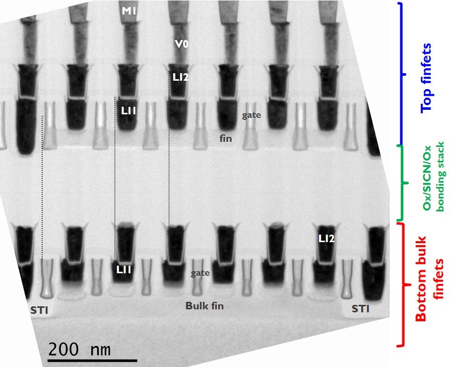
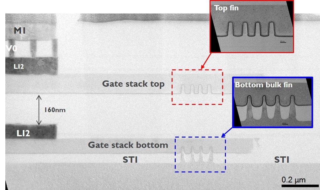
The saturation of Moore’s curve while following systematic downscaling of logic and memory devices has given rise to the biggest challenges involving contacts and interconnects in the chip. The transistors (FinFETs at leading nodes) are getting better and better at smaller dimensions. On the contrary, the shrinking interconnects and contacts at each technology node cause the unwanted resistance-capacitance (RC) delay to increase. Therefore, the chipmakers are exploring new materials to replace conventional tungsten and copper for contacts and interconnects, respectively (see figure below, LINK). At 10 nm, Intel switched over to cobalt for contacts and some, but not all, interconnect layers. Ru is also being explored hugely since Co has some trade-offs as well as higher line resistance (VLSI 2017, Globalfoundries). In fact, there was also news in the market regarding use of Ru implemented in Intel’s 10 nm technology node (TechInsight 2018).
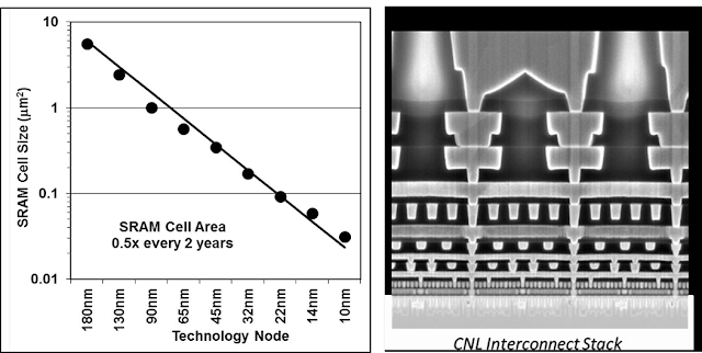
Intel 10nm mid end of line cobalt and copper 12 layer metallization as presented at IEDM December 2017 pre-announcement (LINK, Press kit).

Ru is also an excellent candidate for the electrode capacitor in DRAM applications and gate electrode material in CMOS transistor applications because of its high melting point, high oxidation resistance, and low resistivity. Ruthenium’s lower resistivity and ease of dry etching give it a significant advantage over other noble metals like iridium and platinum. Ru seed-layer deposited as a conformal via liner significantly improves copper adhesion and hinders oxygen diffusion in interconnects and through-silicon-via (TSV) applications. Moreover, ruthenium oxide is conductive and therefore, oxygen diffusion from adjacent materials or processes does not hinder the device performance. Recent research reports the use of ruthenium-based materials as an electrode in ferroelectric applications as well.

Thus, as the main bottleneck of next generation ICs, interconnects and contacts are nowadays the major driving factors of the market of high quality specialty chemicals for the performance or function specific materials or molecules. The physical and chemical properties of a single molecule or a formulated mixture of molecules as well as its chemical composition influence the end product performance extensively. Therefore, unlike the other sub-sectors of the chemical industry, the companies manufacturing and marketing specialty chemicals provide more often than not targeted customer service to innovative individual technical solutions for their customers. 

Since 1964, Strem Chemicals, Inc. has been serving its clients from academic, industrial and government research and development laboratories as well as commercial scale businesses in the pharmaceutical, microelectronic and chemical / petrochemical industries. Strem (Headquarters: Newburyport, Massachusetts, USA) is a high purity specialty chemicals’ manufacturer and supplier. Strem also provides custom synthesis (including high pressure synthesis) and current good manufacturing practice (cGMP) services. With ISO 9001 certification for Quality Management System (QMS) standard and documentation, most of the Strem’s products are reliably of high purity, typically 99%, with some at 99.9999% metals purity. Strem utilizes a comprehensive range of analytical techniques tailored to each product to insure quality because the researchers typically rely on the supplier's quality procedures and documentation, which may kill a great research idea if poorly conducted. All of Strem's catalogs, since inception, have listed “Color and Form” for every product as primary indicators of quality.

More than fifty years of experience in manufacturing inorganic and organometallic chemicals has enabled Stem to expand its product offering of MOCVD, CVD, and ALD precursors. They are continually adding new products for this dynamic and exciting field. Strem’s product range includes:


Most of the available Ru ALD or CVD precursors have issues concerning low vapor pressure and high impurity levels, such as carbon and oxygen, which get incorporated in the films. In addition to that, long incubation times impacting throughput and process controllability, poor film adherence, and non-uniformity in high-aspect ratio structures are some critical limitations of the field. However, ruthenium amidinate precursors such as Bis(N,N’-di-t-butylacetamidinato)ruthenium(II) dicarbonyl (catalog number 44-0056) and others are some of the most promising precursors finding a home in Strem’s product catalog for growing ALD and CVD films. Each amidinate ligand chelates the metal center through two metal-nitrogen bonds. These relatively weak M-N bonds and strong byproduct N-H bonds lead to lower ALD growth temperatures. However, the M-N bonds are strong enough to provide stability to the precursor at the standard temperatures used. Also, since the amidinate ligands chelate to the metal center, they are thermally stable yet have high and self-limited reactivity to water vapor which is essential for ALD. Amidinates do not have any oxygen-metal bonds thus enabling the deposition of metallic films with very low oxygen content in the film and at the interface with the sub-layer.

ALD thin-films deposited using Bis(N,N’-di-t-butylacetamidinato)ruthenium(II) dicarbonyl exhibit high conductivity, density and purity.  Atomic probe microscopy measurements revealed nearly carbon free crystallites with far less carbon impurity segregated near the grain boundaries. The films also showed very good conformality even inside the trenches with aspect ratios (~40:1) possessing strong adhesion. The precursor was found to be thermally stable in a bubbler at 130°C for months and showed very clean TGA vaporization with only trace residue (0.2%).
---
Promotional Blog for Strem Chemicals, Inc.
Researched, produced & written by BALD Engineering AB, Stockholm, 2018-10-30
Abhishekkumar Thakur, Jonas Sundqvist
www.baldengineering.com