Thursday, April 5, 2018

FREE webinar: Optimising ALD high-k oxides for novel applications

FREE webinar: Optimising ALD high-k oxides for novel applications, 19 April 2018, 15:50 UTC [LINK]


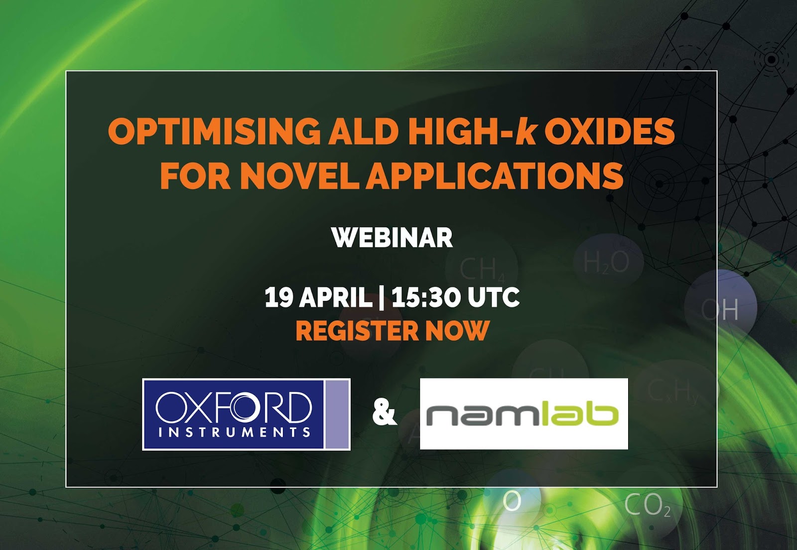
Dr Harm Knoops and special guest speaker, Dr Uwe Schroeder, Deputy Scientific Director from NaMLab GmbH Dresden, Germany, will talk you through the ALD of ferroelectric HfO2 for novel memory applications and the tuning properties of TiO2 and HfO2 by substrate biasing during Plasma ALD.

The webinar will comprise of two talks, with a Q&A session at the end. Register here


Dr.ir. Knoops is the Atomic Scale Segment Specialist  for Oxford Instruments Plasma Technology and holds a part-time researcher position at the Eindhoven University of Technology. His work covers the fields of (plasma-based) synthesis of thin films, advanced diagnostics and understanding and developing plasma ALD and similar techniques. His main goals are to improve and advance ALD processes and applications for Oxford Instruments and its customers. He has authored and co-authored more than 30 technical papers in peer-reviewed journals.  

Dr Uwe Schroeder has held the Deputy Scientific Director position at NaMLab GmbH, Dresden, Germany since 2009. His main research topics are material properties of ferroelectric hafnium oxide and the integration of the material into future devices.

Prior to joining NaMLab, Schroeder was in a Senior Staff Scientist position at Qimonda, previously known as Infineon Technologies (Memory Division) and Siemens Semiconductor before.  At Infineon’s Memory Development Center in Dresden, his research included work on high k dielectric and its integration into DRAM capacitors as a project manager. During this work the so far unknown ferroelectric properties of doped HfO2 based dielectrics were found. He focused on a detailed understanding of these new material properties and their integration into memory devices. 

Schroeder received a Master degree in Physics and a PhD degree in Physical Chemistry field from University of Bonn, Germany including a research visit at UC California, Berkeley and worked at University of Chicago as a post-doctoral researcher.

Wednesday, April 4, 2018

Call for Papers ALD for perovskite-based devices - Symposium C at the E-MRS Fall Meeting 2018

Atomic layer deposition (ALD) for perovskite-based devices - a hot topic to be covered by the Symposium C at the E-MRS Fall Meeting 2018

https://www.european-mrs.com/perovskite-solar-cells-surface-interface-and-materials-aspects-emrs

Atomic layer deposition (ALD) for perovskite-based devices - a hot topic to be covered by the Symposium C at the E-MRS Fall Meeting 2018

ALD of ZrO2 from zirconium tetraiodide and ozone

Please use the free month at ECS and download this excellent paper by Kaupo Kukli et al on probably the best zirconium ALD precursor in the world - behold the Zirconium tetraiodide (ZrI4)! Previously ZrO2 ALD employing ZrI4 has been proven using H2O, H2O/H2O2 and O2 so now the reies is almost compelte - just O2+ missing.

Wikipedia states "The compound was once prominent as an intermediate in the purification of zirconium metal." Refereing to the van Arkel Process, taht is Pyrolysis of zirconium tetraiodide gas by contact of hot wire and that was the first industrial process for the commercial production of pure ductile metallic zirconium. The process was developed by Anton Eduard van Arkel and Jan Hendrik de Boer in 1925, both Dutch chemists. By many this process is a chemical transport process and it relies on two basic chemical reactiosn at elevated temperatures:
M + 2I2 (>400 °C) → MI4
MI4 (1700 °C) → M + 2I2
... and that´s about all the information you need to go ahead and move on to HVM with this one ;-)

Atomic Layer Deposition of Zirconium Dioxide from Zirconium Tetraiodide and Ozone
Kaupo Kukli, Marianna Kemell, Kenichiro Mizohata, Marko Vehkamäki, Kristjan Kalam, Helena Castán, Salvador Dueñas, Joosep Link, Raivo Stern, Mikko Ritala, and Markku Leskelä
 
Abstract : ZrO2 thin films were grown by atomic layer deposition using alternate surface reactions of ZrI4 and O3 precursors in the temperature range of 250–400°C to the thickness in the range of 5–100 nm. The films were dense, continuous, and consisted of mixed monoclinic and metastable polymorphs with significant contribution from cubic ZrO2. The ZrO2 films possessed permittivity up to 19. The capacitor structures based on these films also demonstrated tendency to resistive switching behavior. The ZrO2 films exhibited saturative magnetization under external magnetic fields.

ALD Webinar - Introduction to Beneq Coating Services

ALD Automation Engineer at Picosun

Picosun is a leading supplier of high quality Atomic Layer Deposition (ALD) thin film coating solutions for industries and R&D. Due to the growing interest towards ALD throughout the global industrial scene, we are constantly seeking new people to enforce our highly motivated and skillful organization. We offer you a challenging and versatile job in a dynamic, fast developing high-tech company with a supportive team and innovative spirit. 
In an agile and growing company, you will have a possibility to influence the tools, methods and ways to operate in your field expertise.

We are looking for an addition to our automation team. Previous automation related working experience is not necessity, but eager to learn is essential.

The job includes (the final focus is based on your skill and preference):

- Automation and software design for new and existing ALD tools
- Automation and software product management
- Support R&D and Customer Support in automation and software related issues
- On site automation and software installation in projects with high level of customization
- Automation and software product development and life-cycle management

We expect you to have:

- Education in automation engineering or similar field
- Understanding of IEC 61131 programming standards
- Familiar with PLCs (CodeSys/ TwinCAT3 / Omron or similar)
- Familiar with SCADA systems (TwinCAT3 HMI / InTouch or similar)
- Independent, proactive and versatile approach for development and problem solving
- Mindset for continuous learning, development and high quality
- Fluent communication skills in English
- Good teamwork and co-operation skills
- Willingness to travel (up to 10 weeks per year depending on ongoing projects)

Beneficial features:

- Experience with fieldbus technologies (EtherCAT, Ethernet/IP, DeviceNet)
- Object oriented programming skills
- Higher level software development skills (JavaScript / C# / SQL / HTML)
- Interest in user interface design
- Experience in semiconductor industry
- Experience/understanding of cleanroom environments

The place of work is at our production facilities and office in Masala. It is easily accessible via Kehä III and Route 51 (Länsiväylä) by car or by local train via Masala station.

Please send your application and CV to info@picosun.com. For heading/subject please write Automation Engineer – Picosun Oy.

For additional information, you may contact Teemu Törmänen, teemu.tormanen@picosun.com, +358 40 577 9973.

Monday, April 2, 2018

ECS will host its second Free the Science Week April 2-8, 2018

Get ready to download!
 
Download Content for Free!
Vote
ECS will host its second Free the Science Week April 2-8, 2018, allowing free access to the research content in the ECS Digital Library including the Journal of The Electrochemical Society and the ECS Journal of Solid State Science and Technology.
That means you'll get access to over 141,000 articles and abstracts | mark your calendar
PS: Learn more about Free the Science.

Sunday, April 1, 2018

ALD research and development continuous growth!

There are a number of ways how to track R&D in a technological field besides tracking the number of publications. In the case of ALD you can track the number of delegates visiting the annual International ALD conference. ALD 2016 Ireland had 810 delegates and AVS ALD 2017 in Denver had 950 delegates as far as I know. Since the International ALD conference today has >50% industry delegates this is an indication of a growth in R&D interest from both academics and industry.

You can also look at the annual revenue in sales from ALD wafer processing equipment and here information can be taken from regular updates from Gartner, VLSI Research and the leading ALD OEMS like ASM International who report this in their financial reports. If you plot all those numbers using full range on y-axis into a plot (as a I have done below for 2016 numbers) you can clearly see that ALD R&D represented by number of publications and visitors to the International ALD conference and systems sales are growing hand in hand from 2005 until 2016. You can also see that 2009 was a bad year and it took two years for the ALD geeks to recover fully and get back to the ALD conference in numbers. What you can also see is that the ALD System sales went down already one year before (2008) the big crisis...

2016 numbers and forecasts (BALD Engineering AB)

Most of the ALD OEMs have published annual reports now and it seem that 2017 was a stellar year for ALD systems sales.

Another way to track ALD R&D is to look at patent filing. Either you can come up with a set of key words that you think will appear in ALD patents or you can dig into the patent classes and make it a bit easier for you since to look for trends you don´t necessary need all patents it may just be enough to look for a couple of classes where ALD people are filing.

Last year I compiled this graph below showing ALD precursor patent applications and families and two of the most important events for ALD high-k in high volume manufacturing (HVM) on 300mm wafers using ALD:
  • 2004 : ALD of Al2O3/HfO2 high-k node dielectric by Samsung 90 nm DRAM technology
  • 2007 : ALD of HfO2 gate dielectric by Intel for their 45 nm Logic High-k/Metal Gate stack
(Until all presentations starts with the DRAM reference as 3 years before Logic, I will keep on repeating this fact. Remember "Memory before Logic")

Since it can take quite some time for patents applications to form actual global families it is more intriguing to track the number of applications. So ta da! it follows the ALD conference delegate number quite good (green curve above).

Summer 2017 patent search  (BALD Engineering AB)

So how was 2017 and how many ALD patents are being filed so far 2018 - check it out below and for those of you that have hard time to sleep you can compile this plot on a daily basis by clicking in this LINK. Please note that this graph only contains patent from the CPC class C23C16/45525 and that there are other classes as well that need to be included for a full study. Anyhow it is a good one since it states explicitly Atomic Layer Deposition as coating method.  So keep track on the last data point that today is 140 and if it will reach above 671 by the end of the year or not and before that - how many delegates did go to AVS ALD 2018 in Incheon Korea in July!

2018-04-01 patent search (Patbase.com : LINK)

Just recently I met with Prof. Mikko Ritala in Dresden for the EFDS ALD for Industry and I told him that I have a model to predict the number of delegates for ALD Conference 2024 in Helsinki Finland so at this point my recommendation is to book one of these:


ALD yields large crystalline 2D MoS2 thin films

MRS Bulletin reports: Sheets of molybdenum disulfide (MoS2) just a few atoms thick hold promise for high-performance, flexible electronics as well as optical applications. But one obstacle the two-dimensional (2D) material faces is the lack of an efficient method to make it in large quantities. Researchers at Argonne National Laboratory have now demonstrated that the atomic layer deposition method could be used to make uniform, crystalline MoS2 thin films as large as a standard 300 mm silicon wafer. 

Full article : LINK 
JVSTA Journal article : LINK
ALD Process: molybdenum hexafluoride (MoF6) and hydrogen sulfide at 200 °C

Saturday, March 31, 2018

Tokyo Electron reports on patterning technology for advancements in scaling

If you are interested in the latest patterning technology you should read this excellent online publication by Ken Nawa at the Process Integration Center, Tokyo Electron. Tokyo Electron is one of the top supplier for wafer based advanced etch, deposition and clean (and more) tools for the semiconductor industry. Besides the evolution of semiconductor by scaling technology, he covers all the latest advanced technologies:
  • Introduction of advanced patterning technology and challenges
  • SADP – Scaling by thin film formation on sidewall  
  • SAQP – Scaling by extending SADP technology 
  • SAB – Scaling by etch selectivity to multiple materials

Full article: LINK 


(screen dump form tel.com)


Atomic layer etching of gallium nitride - Free download from JVSTA

If you want to know how to ALE GaN using a standard inductively coupled plasma etch system from Oxford Instruments (Plasmalab 100) you have 30 days to download this excellent JVSTA article from Aalto University, Lund University and Fraunhofer IKTS. Next you will be able to learn first hand from Sabbir at the 16th International Conference on Plasma Surface Engineering, September 17 - 21, 2018, in Garmisch-Partenkirchen, Germany (LINK)

Stay tuned for more publications for this fruitful collaboration!

Atomic layer etching of gallium nitride (0001)
Christoffer Kauppinen, Sabbir Ahmed Khan, Jonas Sundqvist, Dmitry B. Suyatin, Sami Suihkonen, Esko I. Kauppinen, and Markku Sopanen
Journal of Vacuum Science & Technology A 35, 060603 (2017) | Read More 

Sabbir Khan adjusting the first recipe for ALE of Silicon on a Oxford Instruments Plasmalab 100 at Lund Nano Lab in Sweden. Later he transferred the process to Aalto University and successfully ALE:ed GaN up there as well.


Mattson Technology launch Novyka product family for atomic level surface engineering and ultra-selective material removal

FREMONT, Calif., March 08, 2018 (GLOBE NEWSWIRE) -- Mattson Technology introduces Novyka™ product family, the most innovative technology for atomic level surface treatment and ultra-selective etching of extremely thin and delicate materials for continued scaling of 3D logic and memory devices.

“There are significant challenges in scaling with 3D structures for advanced memory and logic chips that include small, narrow, deep and complicated features composed of thin layers of different materials. Among these manufacturing challenges is selective removal of certain layers without damaging or removing other layers and without affecting other features,” said Dr. Subhash Deshmukh, Chief Business Officer of Mattson Technology. “Another challenge is cleaning of these complex structures, as wet chemistry is no longer able to meet the requirements of cleaning the very bottom of the high-aspect ratio features while maintaining device structure integrity.” 
 
(screen dump from mattson.com)
 
“Our new Novyka™ products offer proprietary chemistries in surface cleaning, surface treatment and surface modification. The unique designs of Novyka™ products further extend to enable ultra-high selectivity in removal of thin and delicate layers in 3D device structures,” said Dr. Michael Yang, Executive Vice President and Chief Technology Officer of Mattson Technology. “In addition to delivering the most innovative process solutions to some of the key technical challenges in the industry, Novyka™ products have the lowest running cost, or the best total cost of ownership in their class.”

“We are very excited about the potential of Novyka™ products as we are working closely with several of our most advanced customers on a variety of leading edge applications. With Mattson Technology achieving record revenue and profit in 2017, we continue to relentlessly drive technology innovations and provide uncompromising service to our global customer base,” commented Dr. Allen Lu, CEO and President of Mattson Technology.

Mattson Technology, a Delaware Company, headquartered in Fremont, California, designs, manufactures, markets and supports semiconductor wafer processing equipment. Mattson’s dry strip, plasma etch, rapid thermal processing and millisecond annealing equipment are used in high volume manufacturing by leading memory and logic chip makers around the world. New innovations from Mattson in atomic surface engineering™ address the most critical 3D logic and memory manufacturing challenges. Learn more at www.mattson.com.

Tuesday, March 27, 2018

The Critical Materials Council Conference 2018

For people who think materials matter...
Materials, immediate and future, critical to semiconductor devices
The CRITICAL MATERIALS COUNCIL CONFERENCE 2018
Final Agenda features:
 
Keynote Speaker: David Bloss, VP, Technology and Manufacturing Group Director, Lithography Technology Sourcing, Global Supply Management, Intel Corporation,
"Patterning Challenges and Fab Materials for Future ICs
Also, presenting on Emerging Materials: 
  • Glen Wilk, VP of ALD Products of ASM, providing an insight on High K limits and SAQP challenges
  • Dave Thompson, Sr. Director of Applied Materials, presenting insights on Ruthenium
And focused on Immediate Materials Challenges:
  • Mark Scholefield, Sr. Member of the Technical Staff of GlobalFoundries, providing challenges surrounding silicon wafer quality and associated roadmaps
  • Ken Unfried, Sr. Manager of Linde, providing the latest in issues surrounding neon ad xenon recycling
 ... among a host of other germane and magnetic speakers. The Conference also includes the popular "Not-so-usual Round Tables" with scintillating topics and networking opportunities for all.
 
The CMC Conference provides:
* Updates on market dynamics and regulations
* Trends in the profitable control of all fab materials
* Technology forecasts for future critical materials

Register by April 15th and get entered into a drawing to win a "WiFi Sports Camera."
http://cmcfabs.org/registration/  Courtesy of MegaFluidSystems. 
Click here for the updated agenda
Schedule Details:
Welcome Reception April 25th evening
Sessions I & II, April 26th
Session III, April 27 morning 
Welcome reception, lunch on 26th & coffee/tea breaks are included.


The conference follows the CMC Fabs F2F meeting (on April 24-25) and CMC Members only (Associates and Fabs) Joint Session (on April 25, 2-5pm), located nearby at NXP. For more information about these meetings and/or the Conference, please contact Meena Sher by email by clicking here.

Sunday, March 25, 2018

UPDATED : Report from EFDS ALD for Industry 2018 in Dresden Germany

While we wait for the high class photographs from Martin Knaut, here is a collection of photos and thoughts collected in social media during and after the event. The first days event, the lab tours and tutorials was sponsored by HERALD COST action MP1402 - (LINK).

Dr. Knauts PHOTOS AVAILABLE NOW (LINK)

This year was a success and we grew slightly from last year to 80 participants in the tutorials, more than 90 delegates in total and 18 exhibiting sponsors. Out of the participants more than 70% came for the industry - hope to see more of you next year in April for EFDS ALD for Industry 2019!

Event page (LINK)

Day 1 - Lab tours, Tutorial and Social Event

Tour 1: Fraunhofer IKTS

The Thin Film Technology group at IKTS is engaged in research and development of CVD and ALD technologies for a broad range of applications. Several methods are used:
  • thermal CVD processes at low pressure and atmospheric pressure (LPCVD, APCVD)
  • plasma-enhanced CVD (PECVD)
  • atomic layer deposition (ALD). 
Layer materials like hard coatings, aligned carbon nanotubes (CNT), metal nitrides and dielectrics based on oxides of hafnium, zirconium and titanium and different perovskite materials is the main focus. The applications cover wear-resistant coatings & hard metals, actuating elements, sensors, lithium batteries and energy management and microelectronics.


Pictures form the lab tour as provided by EFDS.

Saturday, March 24, 2018

Measuring Hydrogen, Carbon, Oxygen and Iron Contamination in ALD Films

Contamination in ALD for Semiconductors

Atomic layer deposition (ALD) is a useful technique that can produce films that contain high levels of hydrogen, carbon, oxygen and other metals, which are not desirable elements for semiconductor films. To detect any contamination of these elements in semiconductor films, a number of improve plasma sources in nitride-based ALD grown films can be used. Additionally, X-ray photoelectron spectroscopy (XPS) can also be used to detect accurate composition profiles, however for hydrogen, carbon and oxygen concentrations of 5% or less can become background limited. In cases where the hydrogen, carbon and oxygen profiles are 5% or lower, SIMS analysis is often required.
 
Full article in AZONano as proovided by EAG Laboratories : LINK


ASM International report recovery in the single-wafer ALD market due to strong 3D-NAND fab invest

Almere, The Netherlands, March 22, 2018 ASM International N.V. (Euronext Amsterdam: ASM) today publishes its 2017 Annual Report.

ASMI's Annual Report is also available on the company's website www.asm.com. The Annual Report includes the Corporate Responsibility Report and the Remuneration Report in order to increase the relevancy and quality of reporting to all stakeholders.

ASMI will hold its Annual General Meeting of Shareholders (AGM) on May 28, 2018. The AGM agenda with all related documents will be available in due time.

MESSAGE FROM THE CEO (asm.com LINK)
In 2017 we achieved significant progress against our strategic targets. Our sales benefited from a clear recovery in the single-wafer Atomic Layer Deposition (ALD) market, in particular driven by strong increases in the 3D-NAND segment. During the year we also successfully expanded our position in the epitaxy market with an important tool win from a leading foundry customer. In total, our revenue increased by 23% to a new record level. 


Please check out the financial data at a glance here (LINK).

Thursday, March 22, 2018

NCD announced to provide solar cell ALD equipment to SF-PV

NCD recently shipped the equipment to SF-PV who is a Chinese solar cell manufacturer. This system is (Lucida GS Series + Automation) to increase the efficiency of solar cells by depositing high quality Al2O3 ALD thin films. It will be installed on the site in the end of March and begin production in April.

Lucida GS Series is batch type ALD deposition equipment that forms backside passivation of Al2O3 on multiple wafers and can process more than 4.500 wafers (@ 4nm thickness) of 156mm x 156mm size per an hour. By applying Lucida GS Series in the production of solar cells, customers can dramatically lower the production cost of high efficiency solar cells due to the high-volume productivity, high yield, efficient gas consumption and low maintenance cost compared to competitors. 


(Lucida™ GS series + Automation)

ALD Applications Symposium at the ECS & AiMES Meeting 2018 Cancun

The Call for Papers for the Joint 233rd ECS & AiMES 2018 International Meeting (Sept. 30 – Oct. 4, 2018 in Cancun, Mexico) contains a call for symposium G02 - Atomic Layer Deposition Applications 14

You are cordially invited to submit your abstract. Abstract due date: March 30, 2018.

This symposium will contain:
Tutorials
“Basics of Atomic Layer Etching” by Dr. Thorsten Lill, Lam Research, USA
“ALD precursors for ALD” by Prof. Chuck Winter, Wayne University, USA

Tentative List of Invited Speakers: including
- Mikko Nisula, Aalto University, Finland, ALD/MLD for thin-film Li-ion batteries”
- Cathérine Marichy, University of Lyon, France, “ALD for gas sensing applications”
- Anil Mane, Argonne National Laboratory, USA, “ALD and ALE of 2D materials”
- Riikka Puurunen, Aalto University, Finland, “Learnings from an Open Science Effort: Virtual Project on the History of ALD”
- Alexey Kovalgin, Twente University, Netherlands, “Comparative study of low-temperature III-V nitrides ALD in thermal and radical-enhanced modes”
- Thorsten Lill, Lam Research, USA, “Atomic Layer Etching”
- Geun Young Yeom, SKKU, Korea, “Layer control of 2D-MoS2 by Atomic Layer Etching and its device characteristics”
- Mark Saly, Applied Materials, USA, “Challenges and applications in Atomic Layer Processing”
- Chuck Winter, Wayne University, USA, “Precursors for ALD”
- Ganesh Sundaram, Veeco, “Innovations in ALD”
- Alex Pearse, Modern Electron, USA, “LiPON ALD for Li-ion batteries”
- Neil Dasgupta, University of Michigan, “Interfacial engineering of energy conversion and storage materials by ALD”.

General info on: https://ecs.confex.com/ecs/aimes2018/cfp.cgi
 
ALD Applications Symposium at the ECS & AiMES Meeting 2018

Monday, March 19, 2018

RASIRC Turns Thermal Mass Flow Measurement of Dilute Reactive Gas Species Inside Out

Company features new thermal mass gas sensor at ALD for Industry 2018

San Diego, Calif – March 19, 2018–RASIRC will present an new thermal mass gas sensor for independent measurement of precursor flow rate at the ALD for Industry 2018 conference held in Dresden, Germany March 21 and 22. The presentation will discuss the importance of precursor gas flow measurement independent of carrier gas flow and will provide experimental performance data with hydrogen peroxide gas. The company will also discuss its metal nitride and metal oxide precursor gases in the exhibits area. 
 

Jeff Spiegelman at ALD for Industry last year (EFDS ALD for Industry 2017, 17-18 January Dresden, Germany)
 
RASIRC is a conference sponsor and will also participate in the exhibition. ALD for Industry is sponsored by the European Society for Thin Films (EFDS) and is a topical workshop focused on industrialization and commercialization of ALD for current and emerging markets.

“Process control is crucial for product yields and materials utilization,” said Jeffrey Spiegelman, RASIRC President and Founder. “New RASIRC monitoring technology solves a difficult problem for highly reactive gases, enabling better process stability and lower materials cost.”

RASIRC Brute Peroxide is a novel oxidant that improves passivation and nucleation density at film interfaces when compared to other oxidants. Surface functionalization is denser and initiation is faster using this anhydrous hydrogen peroxide gas compared with alternatives. This high reactivity allows for less chemistry use, and higher throughput due to shorter required purge times.

BRUTE Hydrazine enables low temperature ALD (sub-350°C) . Highly reactive, BRUTE Hydrazine creates uniform metal nitride deposition on 3D surfaces for barrier layers and atmospheric protection.

RASIRC’s Peroxidizer® provides high volumes of reactive H2O2/H2O mixtures for high throughput ALD. This reactive gas generator is ideal for roll-to-roll ALD coatings that require high speed deposition at reduced temperatures.

RASIRC products also include the RainMaker Humidification System (RHS) that generates water vapor for oxidation applications, and the Hydrogen Peroxide Steamer (HPS) for surface cleaning, preconditioning, wet thermal oxidation and residual carbon removal.

About RASIRC

RASIRC specializes in products that generate and deliver gas to fabrication processes. Each unit is a dynamic gas plant in a box—converting common liquid chemistries into safe and reliable gas flow for most processes. First to generate ultra-high purity (UHP) steam from de-ionized water, RASIRC technology can now also deliver hydrogen peroxide gas and hydrazine gas in controlled, repeatable concentrations. RASIRC gas delivery systems, humidifiers, and closed loop humidification systems are critical for many applications in semiconductor, photovoltaic, pharmaceutical, medical, biological, fuel cell, and power industries. Call 858-259-1220, email info@rasirc.com or visit http://www.rasirc.com.

#####

Contacts:

RASIRC
Jeffrey Spiegelman
Phone: 858-259-1220
E-mail: jeff@rasirc.com

Amazing rock n roll ALD machine from Boulder Colorado

Those of you that follow ALD knows that much of the new cool and exciting ALD processes, precursors and technology comes out of Boulder Colorado and especially the Prof. Geroge Group. Some personal favourites and examples are:

- Tungsten ALD
- Low temperature SiO2 catalytic ALD [LINK]
- Implementation of QCM in ALD as a standard tool
- Reverse ALD with new chemistries a.k.a. thermal ALE
- ALD on particles

Obviously many other labs also work hard on these new approaches but somehow the Gerorge Lab always produce that fundamental benchmarking type or research that you tend to return to long after it was published. The best thing is that all the publications are listed and partially available in the long list of publications (LINK) so it is easy to come back later and find the publications.


Just the other day this amazing video of a rock n roll ALD machine from Boulder Colorado was posted on LinkedIn (LINK) by Alexander Yersak, who is a post doc there. Turn on the volume and have a look yourself!


Video downloaded from LinkedIn (LINK)

Check out Alexander Yersak Research Gate profile for access to some of his publications (LINK) lik these ones for example:
Rapid Characterization of Thin Film Dissolution in Water with in Situ Monitoring of Film Thickness Using Reflectometry
Atmospheric pressure spatial atomic layer deposition web coating with in situ monitoring of film thickness

Picosun announces significant repeat sales of P-300F batch ALD cluster tools

ESPOO, Finland, 19th March, 2018 – Picosun Group, a leading provider of Atomic Layer Deposition (ALD) thin film coating technology for global industries, reports of significant repeat sales of PICOSUN™ P-300F production cluster tools to major US industry customers.

Semiconductor components manufactured on silicon and compound semiconductor wafers are crucial in several everyday consumer electronics products as well as in e.g. transport, aerospace, or industrial automation and power applications. Even if the majority of the most common IC components is produced on 300 mm silicon wafers, the sub-300-mm manufacturing is vital and increasingly important especially for the existing and emerging non-silicon-based devices. Wafer materials limited to max. 200 mm diameter such as SiC, GaN, AlN, sapphire, GaAs, LiNbO3, and LiTaO3 offer various benefits over silicon and enable a generation of completely new, advanced and innovative end products.
The PICOSUN™ P-300F ALD system is specially designed for production of IC components such as microprocessors, memories, and hard drives, and manufacturing of power electronics, mixed signal, and MEMS devices such as print heads, sensors, and microphones (LINK).

Picosun’s core competence are cost-efficient, turn-key ALD production solutions for the fast growing More-than-Moore market. The PICOSUN™ P-300F tool is the flagship product for these customers. Specially designed to be run in cluster configuration under constant vacuum to enable fast and efficient high throughput manufacturing, the P-300F tools are connected together and operated in fully automatic mode with a central vacuum robot substrate handling and transfer system. The unique batch flipping mechanism in the P-300F tool is ideal for manufacturing lines where the most of the process steps take place in horizontal geometry. Cassette-to-cassette loading for up to 50 pcs batches of 200/150/100 mm wafers, SEMI S2/S8 certification, and SECS/GEM option for factory host integration make the P-300F the optimal choice for demanding manufacturing needs for e.g. moisture barriers, capacitors, and SAW/BAW filters.

“We at Picosun are very happy of the success of our P-300F cluster tools. Our customers have obtained unparalleled process results in them, and this excellent performance has now resulted in repeat sales of these tools to our key industrial customers. The purity, uniformity, and barrier properties of the ALD films deposited in these systems fulfil the strictest requirements of today’s semiconductor industries, making the PICOSUN™ P-300F the tool of choice for the forerunners of semiconductor manufacturing,” states Juhana Kostamo, Managing Director of Picosun.

Sunday, March 18, 2018

Beneq is looking for a Field Service Engineer

Beneq is a leading supplier of Atomic Layer Deposition (ALD) equipment and thin film coating services, and the world's premier manufacturer of thin film electroluminescent displays. www.beneq.com

LINK: https://my.teamio.com/recruit/public/vacancy?uid=2092cd2f-e73a-4825-bf4d-f6f9416eb50d&rps=254

Field Service Engineer

for testing and commissioning of thin film coating equipment and supporting customers with upgrade and service projects.

Your key responsibilities include:
  • Preparing and testing of the equipment prior to a shipment.
  • Commissioning of the equipment at the customer site.
  • Visiting customers to service the Beneq equipment at the customer site.
  • Giving technical support to customers on-site or by email and phone.
To succeed in this position, you have:
  • Strong engineering or field service engineer background.
  • Good hands-on skills in assembly and service work.
  • Minimum of Bachelor’s degree in a relevant field of engineering.
  • Solid problem-solving skills, customer-oriented mindset and “can do” attitude.
  • Good time management and interpersonal skills.
  • Solid verbal and written English language skills.
  • Ability and willingness to travel globally up to 100-150 days a year.
Additionally, we appreciate:
  • Education and experience in automation and electric installations.
  • Experience of thin film processes.
  • Experience from the semiconductor industry and processes.
  • Experience and education in chemistry.
The position is located in Espoo, Finland. Traveling to customers is often required.
We offer an opportunity to work in an interesting global business and to develop your competences further. You get to work in a dynamic and challenging working environment with a team of professionals.
For more information you can contact Timo Rantasalmi, Head of Customer Services, Thin Film Solutions, phone +358 9 759 9530, e-mail timo.rantasalmi@beneq.com.
Interested? Please send your application including your CV and your salary request as soon as possible. We fill the position as soon as we have found a good candidate.
Key words: field service, engineering, thin films, equipment

Work location
Espoo
Job type
Full-time work
Duration of employment
Permanent

Beneq Oy

Contact person
Eeva Lehtiö

Wednesday, March 14, 2018

MKS has won significant business from a Korean end-user for ALD high flow of ozone systems

Since basically the start of ALD in high volume DRAM manufacturing on 300 mm wafers, ozone has been employed as the co-reactant for ALD of hafnia and zirconia based high-k node dielectrics in the DRAM capacitor memory cell. The ozone concentration directly controls through-put, uniformity and conformalty of the deposited high-k and most importantly also the high-k dielectric performance of the layer including CET/Leakage performance and log term reliability. Please see this early post on details for these processes (LINK)

Just recently MKS Instruments reported (Seeking Alpha Earnings call transcript, LINK) that they won significant business from a Korean end-user for a high flow of ozone systems used in atomic layer deposition to fabricate DRAM memory devices. In addition, MKS reported to have just received a significant suppler award from another major Korean OEM.

MKS further stated that they have made strategic investments with a significant impact on their semiconductor OEM and end-user businesses. Amazingly, the revenue in Korea has increased 250% since 2012. In 2017 alone, their Korea end-user business grew 114%, while the Korea OEM business grew 96%.

Based on this we may assume that high concentration ozone supply i still crucial for the ALD oxide processes in DRAM manufacturing.

MKS Ozone Gas Generators


photo - SEMOZON Ozone Generator

SEMOZON® ozone gas generators and subsystems are the industry standard for compact, high concentration, ultra-clean ozone gas generation. Applications include Atomic Layer Depostion (ALD), Chemical Vapor Deposition (CVD), cleaning and water treatment.

Link to MKS Instrument Ozone products: LINK

MKS Instruments, Inc. is a global provider of instruments, subsystems and process control solutions that measure, control, power, monitor, and analyze critical parameters of advanced manufacturing processes to improve process performance and productivity.  The Company’s products are derived from core competencies in pressure measurement and control, flow measurement and control, gas and vapor delivery, gas composition analysis, residual gas analysis, leak detection, control technology, ozone generation and delivery, RF & DC power, reactive gas generation, vacuum technology, lasers, photonics, sub-micron positioning, vibration isolation, and optics.  MKS’ primary markets include semiconductor capital equipment, general industrial, life sciences, and research.  Additional information can be found at www.mksinst.com.