Thursday, March 1, 2018

2017 was a year of recovery in ALD business driven by 3DNAND according to ASMI

Today was the ASM International NV (OTCQX:ASMIY) Q4 2017 Earnings Conference Call for analysts. The call has been transcripeted by Seeking Alpha (LINK). All in all 2017 was a good year for ALD single wafer market and showed recovery from 2016.  Here is some important take aways from Peter van Bommel - CFO, during teh call:


  • Looking at the company's financial performance, 2017 was a year of recovery in our ALD business. In particular, driven by strong increases in the 3D NAND segment. 2017, we also successfully increased our addressable market in epitaxy as we rolled our first leading high volume manufacturing customer for our new Intrepid too. Initial cost related to new product launches impacted to the gross margin but we still increased our operating profits by 38% in 2017.
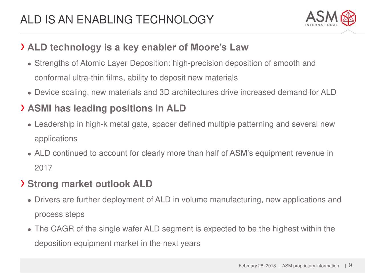
  • In terms of product lines, the key driver was our ALD business, at some distance followed, by Epi and PECVD. Our net sales in 2017 increased by 23% to a new record high of €737 million. Sales were led by our ALD product line, which continued to represent clearly more than half of our equipment revenue.


ASM earnings call slide (sceeen dump from Seeking Alpha LINK)


  • By industry segment, the revenue stream in the fourth quarter was led by memory customers, largely 3D NAND, followed by foundry. Looking at the roadmaps of our customers, the introduction of complex 3D devices structures and new materials and further scaling, will drive the need for more precise deposition of ultrathin and highly comfortable films. This place is the strength of ALD. And as a leader in the single wave of ALD market, our company remains well-positioned to capture the growth expected in this market.

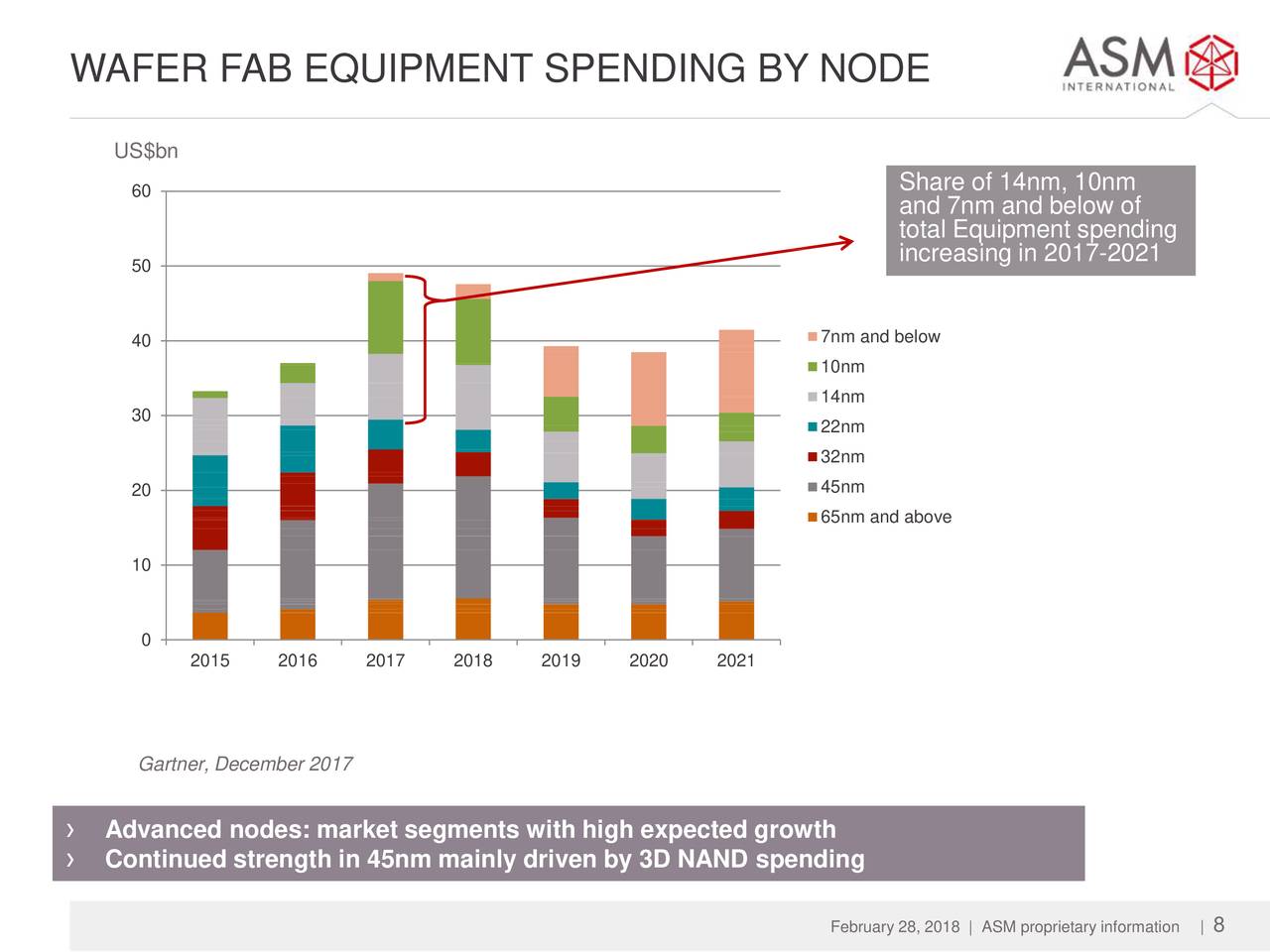
Looking ahead the addressable market for single wafer ALD will grow according to Peter van Bommel since the advanced node share  (14, 10 and 7 nm) will grow to roughly 50% in revenue by 2020-2021 of the total wafer fab equipment spending, when ASM expect the single wafer ALD market to reach  USD 1.5 billion annual revenue (see graph below, Gartner Dec 2017).


ASM earnings call slide (sceeen dump from Seeking Alpha LINK

Not touched upon too much was the Large Batch furnace segment which is dominated by the competitors Tokyo Electron and Hitachi Kokusai. This segment is however much smaller than the single wafer ALD segement, maybe 70:30 ratio or so. The patent disagreement with the Hitachi Kokusai was briefly mentioned but nothing substantial was said since it is an ongoing issue (LINK).


Beneq offers online training in Atomic Layer Deposition

Train yourself online on ALD  - Introducing Beneq Thin Film Solutions webinar series


As experts of Atomic Layer Deposition and thin film coatings, we get a lot of questions about ALD from our customers and partners as well as students and other people with an interest in nanotechnology. The questions and information requests range from very general questions about the ALD technology and its application possibilities to extremely detailed thin film research problems. 
 
 
We will of course try to help the best we can, but it is not always possible to answer personally to everybody, which is why we try to share information about the benefits of ALD in our blog and the technology and research pages of our website.
 
1. Beneq TFS 200 ALD research equipment - Options and Upgrades
Wednesday, March 21st at 3.00 PM EET

In this webinar, Timo Rantasalmi, Head of Customer Services, will walk you through the available option and upgrades with concrete examples of their use and benefits.

2. Introduction to Beneq Coating Services
Wednesday, April 4th at 3.00 PM EET

In this webinar, Dr. Erik Østreng, Head of Coating Services, will explain the benefits of using Beneq Coating Services, introduce the typical coating service solutions and tell you how to get started.

Beneq Webinar Page for full details LINK


Monday, February 26, 2018

ALD/CVD Chemielaborant/in bei Fraunhofer IKTS in Dresden

Die Fraunhofer-Gesellschaft ist die führende Organisation für angewandte Forschung in Europa. Unter ihrem Dach arbeiten 72 Institute und Forschungseinrichtungen an Standorten in ganz Deutschland. Mehr als 25 000 Mitarbeiterinnen und Mitarbeiter erzielen das jährliche Forschungsvolumen von 2,3 Milliarden Euro. Davon fallen knapp 2 Milliarden Euro auf den Leistungsbereich Vertragsforschung. Rund 70 Prozent dieses Leistungsbereichs erwirtschaftet die Fraunhofer-Gesellschaft mit Aufträgen aus der Industrie und mit öffentlich finanzierten Forschungsprojekten. Internationale Kooperationen mit exzellenten Forschungspartnern und innovativen Unternehmen weltweit sorgen für einen direkten Zugang zu den wichtigsten gegenwärtigen und zukünftigen Wissenschafts- und Wirtschaftsräumen.

In der Arbeitsgruppe Dünnschicht-Technologien werden hauptsächlich chemische Gasphasenabscheidung (CVD) für verschiedene Anwendungsfelder eingesetzt bzw. entwickelt. Dabei kommen die Verfahren thermische CVD-Prozesse bei reduziertem oder Atmosphärendruck (LPCVD, APCVD), plasmagestütztes CVD (PACVD) und Atomlagenabscheidung (ALD) zum Einsatz. Werkstoffseitig stehen Hartstoffschichten, Schichten aus gerichteten Carbon Nanotubes (CNT) und nanoskalige Dielektrika auf der Basis von Hafnium-, Zirkon- und Titanoxiden sowie von Perowskiten im Mittelpunkt. Die Anwendungen reichen vom Verschleißschutz über die Aktorik, Sensorik, Batterie- und Energietechnik bis hin zur Mikroelektronik. Die Herstellung neuer Dünnschichtmaterialien erfordert auch die Modifizierung bekannter bzw. die Entwicklung neuer CVD-Technologien. Dies umfasst den Test neuer Precursorsysteme sowie die Durchführung detaillierter Parameterstudien. Unterstützt werden die Untersuchungen durch thermodynamische Berechnungen und durch eine umfassende Charakterisierung von Zusammensetzung, Struktur und Eigenschaften der Schichten.

Künftig umfassen Ihre Aufgaben hierbei
  • Eigenständiger Aufbau, Betrieb und Wartung von Laboraufbauten und Versuchsdurchführung nach Ablaufplan
  • Mitarbeit bei der Auswahl und Definition der wissenschaftlichen Ausrüstung und Chemikalien
  • Anpassung der Laboranlagen an Projekterfordernisse
  • Unterstützung bei der Fehlerbehebung an Anlagen
  • Bereitstellung und Pflege technischer Dokumentationen
  • Auswahl und Koordination externer und interner Lieferanten und Dienstleister
  • Bestellung von Bauteilen und Wartung von für den Anlagenbetrieb notwendigen Zusatzgeräten

Saturday, February 24, 2018

ASM International announces response to Hitachi Kokusai´s counterclaim

ASM International N.V. (Euronext Amsterdam: ASM) today responds to press reports of a patent infringement suit against ASM filed by Hitachi Kokusai in Federal District Court for the District of Oregon on February 20, 2018. The claim follows an earlier suit for patent infringement filed by ASM against Hitachi Kokusai and ASM's earlier initiation of an arbitration against Hitachi Kokusai alleging breach of a license agreement between the parties. ASM will diligently prosecute its cases against Hitachi Kokusai and will vigorously defend against Hitachi Kokusai's claims, which, ASM believes lack merit.

In 2007, ASM and Hitachi Kokusai entered into a licensing agreement, according to which ASM granted usage of its ALD patents in the field of use of batch ALD to Hitachi Kokusai.

On August 30, 2017, ASM initiated an arbitration with the American Arbitration Association against Hitachi Kokusai for breach of the license agreement between the parties. It is not yet known when the arbitration will be completed. 
 

Following the expiration of the parties' patent license agreement, ASM filed, on December 1, 2017, a suit for patent infringement against Hitachi Kokusai and its U.S. subsidiary in the U.S. District Court for the Northern District of California. ASM asserted three patents. ASM has requested both an injunction and monetary damages.

CMC Conference 2018 - a Critical Event for Semiconductor Materials

Critical Event for Semiconductor Materials
CMC Conference Update
This year's Critical Materials Conference features: 
 
Keynote Speaker: David Bloss, VP, Technology and Manufacturing Group Director, Lithography Technology Sourcing, Global Supply Management, Intel Corporation, presenting 
"Patterning Challenges and Fab Materials for Future ICs"
 
Also Featuring:   
  • Glen Wilk, VP, ALD Products, ASM
    • "ALD Materials Integration Challenges"
  • Risto Puhakka, President, VLSI Research
    • "OEM Markets and Materials Trends"
  • Michelle Garza, Sr. R&D Chemist, Fujimi
    • "Cobalt CMP Post Cleans; Wet Cleans Compatibility"
  • Ken Unfried, Sr. Technologist, Linde
    • "Neon and Xenon Recycling"
  • Dave Thompson, Director, Applied Materials
    • "Ruthenium Integration"
and the popular Not-so-unusual Round Table Session - a highly differentiated program, with networking opportunities for all attendees. 
The CMC Conference provides:
* Updates on market dynamics and regulations
* Trends in the profitable control of all fab materials
* Technology forecasts for future critical materials

Register now for the early-bird rate of $375 by March 15th: http://cmcfabs.org/cmc-events/.
Click here for the updated agenda
Schedule Details:
Welcome Reception April 25th evening
Sessions I & II, April 26th
Session III, April 27 morning 
Welcome reception, lunch on 26th & coffee/tea breaks are included.


The conference follows the CMC Fabs F2F meeting (on April 24-25) and CMC Members only (Associates and Fabs) Joint Session (on April 25, 2-5pm), located nearby at NXP. For more information about these meetings and/or the Conference, please contact Meena Sher by email by clicking here.
Early-Bird Registration by March 15
$375
Standard Price $450

Tuesday, February 20, 2018

ALD Development Engineer at Encapsulix S.A. in Provence area in the South-East of France

A full time position as a development engineer is available at Encapsulix SAS. (HTTP://www.encapsulix.com). Encapsulix is a fast growing supplier of ultra fast, large area ALD manufacturing and R&D equipment that serve the thin film barrier and encapsulation needs for the OLED lighting and display, photovoltaic, data storage, architectural glass, and generic large area electronic markets. Encapsulix headquarters and application laboratory are located in Provence, south of France.

Personal Specification

The candidate should at least have a Master Degree in Mechanical or Electrical Engineering, Material Science, Physics or Chemistry ; A professional experience with development , utilization, and/or maintenance of vacuum equipment and or metrology.

The selected candidate will be responsible for development of certain hardware (system and subsystem level), control algorithms and deposition processes related to high speed Atomic Layer Deposition. Relevant technical skills include the design, sourcing and test of mechanical parts, a working knowledge of subsystems such as vacuum systems, thermal control systems and thin film characterization and related metrology. Experience in industrial R&D and product development is preferred.

Candidates should demonstrate enthusiasm and are expected to take ownership of their part of the project for on-time/in budget/ in spec delivery in a high pace/high tech manufacturing environment. They should demonstrate a solid technical background and the ability to rapidly acquire new technical skills. This position requires extensive interactions with customers, development partners and suppliers. Excellent written and oral communication skills and an ability to perform the work independently are essential.

They should also be willing to travel for extended periods of time in Europe, North America and East Asia. Full professional fluency in English is expected. Activities within the scope of certain government related collaborations may require a background check by third parties.

Location

The position will be based in the Provence area in the South-East of France. In recent years, the region has developed a vibrant high tech industry in the fields of microelectronics, aerospace, advanced optics and renewable energies.

Appointment and Starting Date

This position offers full-time employment. The starting date will be March 1st, 2018 at the earliest.

Information and Application

For more information on the position, please contact Jacques Kools (jkools@encapsulix.com). To apply, please send an application letter, along with curriculum vitae with the names of two professional references who can be contacted.

Monday, February 12, 2018

Gain a 'Material' Advantage - CMC Conference 2018

Gain a 'Material' Advantage
CMC Conference 2018
The 3rd Critical Materials Council (CMC) Conference is a 2-day event happening April 26-27 in Phoenix, AZ, where leading semiconductor fabs and suppliers discuss ways to resolve issues related to materials, manufacturing and global supply-chains. Speakers from CMC Members such as Intel, Samsung, and TI, along with analysts and experts from OEMs and materials-suppliers will provide presentations at this public event, which follows the private members-only CMC meeting. Benchmark your world here.

Keynote speaker David Bloss, VP of Technology and Manufacturing Group, and Director of Lithography Technology Sourcing in Global Supply Management, Intel Corp., will start the three-session event exploring:
* Updates on market dynamics and government regulations,
* Trends in the profitable control of all fab materials, and
* Technology trends & forecasts for future critical materials.

Register now for the early-bird rate of $375 by March 15th: http://cmcfabs.org/cmc-events/.
Click here for the updated agenda
CONFERENCE DETAILS

Welcome Reception April 25th evening
Sessions I & II, April 26th
Session III, April 27 morning 
Welcome reception, lunch on 26th & coffee/tea breaks are included.


The conference follows the CMC Fabs F2F meeting (on April 24-25) and CMC Members only (Associates and Fabs) Joint Session (on April 25, 2-5pm), located nearby at NXP, Chandler, AZ.  For more information about these meetings and/or the Conference, please contact Meena Sher by email by clicking here.
Early-Bird Registration by March 15
$375
Full Price $450

Saturday, February 10, 2018

NCD signed a contract to supply ALD equipment for PERC cells with JA Solar in China

NCD has recently signed a contract to supply ALD equipment for manufacturing high efficiency PERC cells with JA Solar, a large solar cell manufacturer in China. This equipment is Lucida GS Series that offers higher efficiency to crystalline silicon solar cells by depositing high quality Al2O3 ALD thin films on the back side of wafers. 
 
Lucida GS Series is a batch type ALD deposition system that forms backside passivation of Al2O3 on multiple wafers and can process more than 4.500 wafers (@ 6nm thickness) of 156mm x 156mm size per an hour. By applying Lucida GS Series in the production of solar cells, customers can dramatically lower the production cost of high efficiency solar cells due to the high-volume productivity, high yield, efficient gas consumption and low maintenance cost compared to competitors. Based on these advantages and excellence, NCD is confident that the Lucida GS Series will become essential equipment for ALD process application for manufacturing high efficiency solar cells.

NCD will continue to make efforts to become the world’s best specialized company that leads ALD technologies in the future.
< Lucida GS Series >


Spatial atomic layer deposition for coating flexible porous Li-ion battery electrodes

Here is important step forward in fast roll to roll processing of Li-battery electrodes using fast spatial ALD from CU Boulder, Colorado. Spatial ALD (SALD) is based on separating the precursors and inert gas purges in space rather than in time and therefore the deposition rates up to a hundred times faster are achievable. SALD can be performed at ambient atmosphere and therefore is a cheaper technology due to less need of expensive vacuum technology compared to conventional low pressure ALD.

High speed and low cost of ownership opens the door to high volume manufacturing of bulk quantities of energy materials for applications including solar energy, energy storage, or smart windows. Previously ALD Nanosolutions has announced a Spatial ALD technology for conformal encapsulation of ALD on powder material like for instance Li-battery cathode powder (LINK). A good overview of Spatial ALD for energy applications is this review paper by David Muñoz-Rojas et al: "Spatial Atomic Layer Deposition (SALD), an emerging tool for energy materials. Application to new-generation photovoltaic devices and transparent conductive materials" https://doi.org/10.1016/j.crhy.2017.09.004 [OPEN ACCESS]

Please find the JVSTA abstract below for the recent article form Boulder:

Thursday, February 8, 2018

Recent Solar Cell and Battery Materials Articles in JVSTA

Quite a bunch of interesting ALD papers in JVSTA!


Laser ablation compatible substoichiometric SiOx/SiNy passivating rear side mirror for passivated emitter and rear thin-film crystalline silicon solar cells,  Félix Gérenton, Fabien Mandorlo, Erwann Fourmond, Marine Le Coz, Danièle Blanc-Pélissier, Mustapha Lemiti |  Read More


Plasma-enhanced atomic layer deposition of vanadium phosphate as a lithium-ion battery electrode material,  Thomas Dobbelaere, Felix Mattelaer, Philippe M. Vereecken, Christophe Detavernier |  Read More


Performance and durability of broadband antireflection coatings for thin film CdTe solar cells,  G erald Womack, Piotr M. Kaminski, Ali Abbas, Kenan Isbilir, Ralph Gottschalg, John Michael Walls |  Read More

Application of microcracked columnar TiO2 thin films deposited by DC hollow cathode plasma jet in dye-sensitized solar cells,  Roman Perekrestov, Pavel Kudrna, Stanislav Danis, Milan Tichý, Igor Bieloshapka, Rodica Vladoiu |  Read More

Optimizing AlF3 atomic layer deposition using trimethylaluminum and TaF5: Application to high voltage Li-ion battery cathodes,   David H. K. Jackson, Masihhur R. Laskar, Shuyu Fang, Shenzhen Xu, Ryan G. Ellis, Xiaoqing Li, Mark Dreibelbis, Susan E. Babcock, Mahesh K. Mahanthappa, Dane Morgan, Robert J. Hamers, Thomas F. Kuech |  Read More

Single vacuum chamber with multiple close space sublimation sources to fabricate CdTe solar cells,  Drew E. Swanson, Jason M. Kephart, Pavel S. Kobyakov, Kevin Walters, Kevan C. Cameron, Kurt L. Barth, Walajabad S. Sampath, Jennifer Drayton, James R. Sites |  Read More

Spatial atomic layer deposition on flexible porous substrates: ZnO on anodic aluminum oxide films and Al2O3 on Li ion battery electrodes,   Kashish Sharma, Dmitri Routkevitch, Natalia Varaksa, Steven M. George |  Read More
 
Atomic layer deposition of tin oxide using tetraethyltin to produce high-capacity Li-ion batteries,  Denis V. Nazarov, Maxim Yu. Maximov, Pavel A. Novikov, Anatoly A. Popovich, Aleksey O. Silin, Vladimir M. Smirnov, Natalia P. Bobrysheva, Olga M. Osmolovskaya, and Michail G. Osmolovsky, Aleksandr M. Rumyantsev |  Read More

Atomic layer deposition of NiS and its application as cathode material in dye sensitized solar cell,   Neha Mahuli, Shaibal K. Sarkar |  Read More

Effect of the cadmium chloride treatment on RF sputtered Cd0.6Zn0.4Te films for application in multijunction solar cells,  Tushar M. Shimpi, Jason M. Kephart, Drew E. Swanson, Amit H. Munshi, Walajabad S. Sampath, A. Abbas, John M. Walls |  Read More

Wednesday, February 7, 2018

CRITICAL EVENT FOR SEMI MATERIALS - April 26-27 Phoenix

The Critical Materials Council (CMC) Conference is a 2-day event, happening April 26-27 in Phoenix, AZ, providing actionable information on materials and supply-chains for current and future semiconductor manufacturing. Speakers from CMC Members such as GlobalFoundries, Intel, Samsung, and TI, along with analysts and experts from OEMs and materials-suppliers will explore issues associated with using materials such as cobalt and ruthenium in commercial fabs. Evening receptions and lunch allow for networking time with industry leaders.

Keynote speaker David Bloss, VP of Technology and Manufacturing Group, and Director of Lithography Technology Sourcing in Global Supply Management, Intel Corp., will start the three-session event exploring:

* Updates on market dynamics and government regulations,
* Trends in the profitable control of all fab materials, and
* Technology forecasts for future critical materials.

Join us in the Phoenix area: http://cmcfabs.org/cmc-events/