Friday, January 5, 2018

Memory chips led the way in 2017 boosting a 22% record semiconductor growth in revenue

Memory chips (DRAM & FLASH) led the way in 2017 boosting a 22% record semiconductor growth in revenue. Samsung Electronics became the number 1 in overall semiconductor sales for the first time, displacing Intel, which had held the top spot in sales every year since 1992. 


EE Times reports : Semiconductor sales grew by 22 percent to reach a record $419.7 billion — with memory chips leading the way — according to a preliminary estimate by market research firm Gartner.

Gartner (Stamford, Conn.) estimates that increased sales of memory chips due to shortages of NAND flash and DRAM accounted for about two-thirds of overall chip market growth in 2017. Memory also become the single largest semiconductor products category last year, according to the firm.

Full story: LINK


Gartener 2016 to 2017 revenue change for Top 10 Semiconductor companies [replotted]

Thursday, January 4, 2018

Call for Abstracts - AVS 18th International Conference on Atomic Layer Deposition (ALD 2018)


The  AVS 18th International Conference on Atomic Layer Deposition (ALD 2018)  featuring the  5th International Atomic Layer Etching Workshop (ALE 2018)  will be a three-day meeting dedicated to the science and technology of atomic layer controlled deposition of thin films and now topics related to atomic layer etching. The conference will take place Sunday, July 29-Wednesday, August 1, 2018 , at the Songdo Convensia in Incheon, South Korea.

As in past conferences, the meeting will be preceded (Sunday, July 29) by one day of tutorials and a welcome reception. Sessions will take place (Monday-Wednesday, July 30-August 1) along with an industry tradeshow. All presentations will be audio-recorded and provided to attendees following the conference (posters will be included as PDFs). Anticipated attendance is 600+.

Key Deadlines:
Abstract Submission Deadline: February 16, 2018
Author Acceptance Notifications: April 9, 2018
Student Award Applications Deadline: May 1, 2018
Early Registration Deadline: June 1, 2018
Hotel Reservation Deadline: June 26, 2018
JVST Special Issue Deadline: September 5, 2018

Wednesday, January 3, 2018

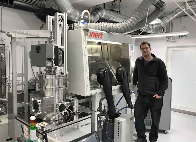
Picosun and Inert has made a new glovebox-ALD install at the Chemical and Technical Institute in Prague

Picosun and Inert has made a new glovebox-ALD install at the Chemical and Technical Institute, Prague. The Inert box is integrated with a R-200 tool for Atomic Layer Deposition of platinum and metal oxides.

Check out the details below!


Cornell University fabricate cell-sized origami robots by an ALD & graphene nanotechnology

Cornell University reports that one of their researcher teams has made a robot exoskeleton that can rapidly change its shape upon sensing chemical or thermal changes in its environment. And, they claim, these microscale machines – equipped with electronic, photonic and chemical payloads – could become a powerful platform for robotics at the size scale of biological microorganisms. Their work is outlined in “Graphene-based Bimorphs for Micron-sized, Autonomous Origami Machines,” published Jan. 2 in Proceedings of the National Academy of Sciences. Miskin is lead author; other contributors included David Muller, the Samuel B. Eckert Professor of Engineering, and doctoral students Kyle Dorsey, Baris Bircan and Yimo Han. [Graphene-based bimorphs for micron-sized, autonomous origami machines. Marc Z. Miskin et al (2018), PNAS https://doi.org/10.1073/pnas.1712889115 ]

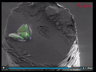
Please check out this interview video for more amazing details - some snapshots are given below in  the form of screen dumps from vimeo [LINK]


The bimorph is built using atomic layer deposition of atomically thin layers (2 nm) of silicon dioxide onto aluminum over a cover slip – then wet-transferring a single atomic layer of graphene on top of the stack. The result is the thinnest bimorph ever made. [Vimeo Screen dump]
 

Processing has been taken place in Cornell University Clean room - Cornell NanoScale Facility for Science and Technology, here showing the ALD reactor and rpocessing of the SiO2 layer (Oxford Instruments, FlexAl) [Vimeo Screen dump]


The researchers can fabricate many different forms of origami shapes ranging from simple tetrahedrons to cubes and helix shaped objects [Vimeo Screen dump]


With this new amazing technology, the Cornell rersearchers are developing robotic ‘exoskeleton’ for electronics with integrated microchips. [Vimeo Screen dump]


Get back to work - SEMI projects continued boom in fab equipment spending for 2018

MILPITAS, Calif. ─ January 2, 2018 ─ The year-end update to the SEMI World Fab Forecast report reveals 2017 spending on fab equipment investments will reach an all-time high of $57 billion. High chip demand, strong pricing for memory, and fierce competition are driving the high-level of fab investments, with many companies investing at previously unseen levels for new fab construction and fab equipment. See figure 1.
World Fab Forecast Figure 1
Figure 1


The SEMI World Fab Forecast data shows fab equipment spending in 2017 totaling US$57 billion, an increase of 41 percent year-over-year (YoY). In 2018, spending is expected to increase 11 percent to US$63 billion.

While many companies, including Intel, Micron, Toshiba (and Western Digital), and GLOBALFOUNDRIES increased fab investments for 2017 and 2018, the strong increase reflects spending by just two companies and primarily one region.

Tuesday, January 2, 2018

Single Atomic Layer Ferroelectric on Silicon by PVD ZrO2


A team of mainly US based researchers from (Yale, MIT, Université de Genève and Globalfoundries) have been able to scale down ferroelectric ZrO2 to only one atomic layer on silicon using PVD. This record breaking thin monolayer ferroelectric allows for more aggressively scaled devices than bulk ferroelectrics as compared to the most current 5–10 nm thick layers based on e.g. Si:HfO2 and HfZrOx. 

They found that:
  • single atomic layer ZrO2 exhibits ferroelectric switching behavior when grown with an atomically abrupt interface on silicon
  • ZrO2 gate stack demonstrate that a reversible polarization of the ZrO2 interface structure couples to the carriers in the silicon.
Single Atomic Layer Ferroelectric on Silicon
Mehmet Dogan, Stéphanie Fernandez-Peña, Lior Kornblum, Yichen Jia, Divine P. Kumah, James W. Reiner, Zoran Krivokapic, Alexie M. Kolpak, Sohrab Ismail-Beigi, Charles H. Ahn, and Frederick J. Walker

Nano Lett., Article ASAP, DOI:10.1021/acs.nanolett.7b03988

Abstract: A single atomic layer of ZrO2 exhibits ferroelectric switching behavior when grown with an atomically abrupt interface on silicon. Hysteresis in capacitance–voltage measurements of a ZrO2 gate stack demonstrate that a reversible polarization of the ZrO2 interface structure couples to the carriers in the silicon. First-principles computations confirm the existence of multiple stable polarization states and the energy shift in the semiconductor electron states that result from switching between these states. This monolayer ferroelectric represents a new class of materials for achieving devices that transcend conventional complementary metal oxide semiconductor (CMOS) technology. Significantly, a single atomic layer ferroelectric allows for more aggressively scaled devices than bulk ferroelectrics, which currently need to be thicker than 5–10 nm to exhibit significant hysteretic behavior (Park, et al. Adv. Mater. 2015, 27, 1811).

Reprinted with permission from (Single Atomic Layer Ferroelectric on Silicon, M. Dogan et al, Nano Letters, Dec 2017). Copyright (2018) American Chemical Society.

High‐resolution STEM image and EDX intensity profiles of Si, Al and Zr. The Supporting Information is available free of charge on the ACS Publications website at "Single Atomic Layer Ferroelectric on Silicon" https://figshare.com/collections/Single_Atomic_Layer_Ferroelectric_on_Silicon/3961401

General Motors and Forge Nano has co-developed ALD technology for lithium batteries

According to recent news releases General Motors and Forge Nano has co-developed and been rewarded for ALD for lithium battery technology featuring:
  • ultrathin (thickness < 5nm) multifunctional hybrid coatings and processes.
  • solutions to critical issues involved with gas generation, manganese dissolution induced capacity loss and safety issue associated with polymeric separators.
  • scale-up production and commercialization of this innovation for both automotive and non-automotive applications.
  • semi-continuous ALD systems (the tall pilot-scale stack, as well as the large single-cycle stack), have the production capacity of more than 1 MT/day, making it possible to implement the advanced surface coating technologies into the next generation of lithium ion batteries.
 
Background information:

LOUISVILLE, CO - Forge Nano, Louisville, Colorado, recently won a 2017 R&D 100 Award as co-developer with General Motors for the development of the Ultrathin Multifunctional Hybrid Coatings and Processes. The R&D 100 Awards have served as an innovation awards program for the past 55 years, honoring great R&D pioneers and their revolutionary ideas in science and technology.

“Forge Nano was founded with a vision to deploy precision nano-coatings to make many other technologies safer, less expensive and more efficient. That vision is now a reality, and it is extremely gratifying to be honored by the R&D 100 Awards for introducing one of 2017’s most innovative and influential technology solutions,” said Forge Nano Founder and CEO Dr. Paul Lichty, who accepted the award at the R&D 100 Conference in Orlando, Florida.

Forge Nano launched in 2013 with breakthrough technology that makes nano-coatings fast, affordable and scalable in manufacturing. The company specializes in nano-coatings and atomic film deposition, serving functions from corrosion resistance to electrical insulation or conduction. As demands for next-generation materials become more and more extreme, nano-engineered surface coatings can fulfill the need for enhanced properties and precise characteristics.


The R&D 100 Award - Ultrathin multifunctional hybrid coatings and processes (LINK)

The majority of battery failure initiates from active material surfaces in the electrodes. Surface coatings, as an effective mitigating strategy, have been widely applied into battery material manufacturing process to protect active materials. Conventional coating technologies, such as chemical vapor deposition, physical vapor deposition and wet chemistry, typically generate non-uniform coating particularly on nano-sized particles. The thickness control becomes difficult, and the thicker coating typically induce high much impedance. To tackle this challenge, General Motors—a pioneer in applying surface coating using the Atomic Layer Deposition (ALD) technique—has developed several Ultrathin multifunctional hybrid coatings and processes. These ultrathin (thickness < 5nm) multifunctional coatings solve critical issues involved with gas generation, manganese dissolution induced capacity loss and safety issue associated with polymeric separators. Forge Nano has developed the technologies that enable scale-up production and commercialization of this innovation for both automotive and non-automotive applications. Their semi-continuous ALD systems (the tall pilot-scale stack, as well as the large single-cycle stack), have the production capacity of more than 1 MT/day, making it possible to implement the advanced surface coating technologies into the next generation of lithium ion batteries.

Monday, January 1, 2018

HHV launch ALD System based on technology transferred from IIT Bombay

Hind High Vacuum Co. Pvt. Ltd. (HHV), a vacuum science and technology company with major clients like HAL, ISRO, BARC, Titan etc, announced the launch of its first indigenously developed Atomic Layer Deposition (ALD) System based on technology transferred from IIT Bombay. This tool was developed entirely by HHV’s Thin Film Technology Division out of its Bengaluru facility as a part of the company’s on-going ‘Make in India’ initiative.


A picture of the ALD 150 system, which seems to be a top loaded tool very similar in layout to e.g. a CNT Savannah. Judging by the name this is a 150 mm system (picture from HHV webpage)

Full story: HHV develops Atomic Layer Deposition System based on technology transferred from IIT Bombay

Press release: LINK

Link to HHV ALD product page: LINK

Encapsulation of homogeneous catalysts in mesoporous materials by diffusion limited ALD

Researches from the Chinese Academy of Sciences demonstrate ALD encapsulation of metal complexes into nanochannels of mesoporous materials is. The pore size of the hollow plug is precisely controlled on the sub-nanometer scale by the number of ALD cycles to fit various metal complexes with different molecular sizes. They claim that this ALD-assisted encapsulation method can be extended to the encapsulation of other homogeneous catalysts into different mesoporous materials for various heterogeneous reactions. Please find the paper below!
Beautiful TEM analysis of carbon nanofibers that have beencoated with 400 cycles TiO2 (supporting information, LINK)
Reference: Zhang, S., Zhang, B., Liang, H., Liu, Y., Qiao, Y. and Qin, Y. (2017), Encapsulation of Homogeneous Catalysts in Mesoporous Materials Using Diffusion-Limited Atomic Layer Deposition. Angew. Chem. Int. Ed.. doi: 10.1002/anie.201712010

Picture from Tweet above

Purdue University demonstrate negative capacitance MoS2 transistors using ferroelectric HfZrOx

WEST LAFAYETTE, Ind. –  Researchers have experimentally demonstrated how to harness a property called negative capacitance for a new type of transistor that could reduce power consumption, validating a theory proposed in 2008 by a team at Purdue University.

The researchers used an extremely thin, or 2-D, layer of the semiconductor molybdenum disulfide to make a channel adjacent to a critical part of transistors called the gate. Then they used a “ferroelectric material” called hafnium zirconium oxide to create a key component in the newly designed gate called a negative capacitor.

A new type of transistor (a) harnesses a property called negative capacitance. The device structure is shown with a transmission electron microscopy image (b) and in a detailed “energy dispersive X-ray spectrometry” mapping (c). (Purdue University photo/Mengwei Si)

Capacitance, or the storage of electrical charge, normally has a positive value. However, using the ferroelectric material in a transistor’s gate allows for negative capacitance, which could result in far lower power consumption to operate a transistor. Such an innovation could bring more efficient devices that run longer on a battery charge.

Aveni extends copper interconnects to 5nm and below for BEOL integration employing ALD TaN & CVD Co barrier/seed

Recently at IEDM 2017 IBM announced that copper is here to stay and can continue to be scaled for the future back end of line (BEOL) interconnects - 20 Years of Cu BEOL in Manufacturing, and its Future Prospects (Invited), D. Edelstein, IBM TJ Watson Research Center (LINK)

Before the actual copper plating process, the advanced dual-damascene structures for interconnects employ two very important conformal deposition processes :
  • an atomic layer deposition tantalum nitride (ALD TaN) copper diffusion barrier
  • a thin chemical vapor deposition cobalt (CVD Co) liner
More detailed information on Cobalt CVD for barrier/seed and selective encapsulation of copper from the leader Applied Materials can be found here (LINK).

According to a press release below (LINK), Aveni has announced it has obtained results that support the continued use of copper in the BEOL for advanced interconnects, at and beyond the 5nm technology node. Aveni is a French developer and manufacturer of wet deposition technologies and chemistries for 2D interconnects and 3D through silicon via packaging. The company was originally founded in 2001 as a spinoff from the Commissariat à l’énergie atomique et aux énergies alternatives (CEA) to develop and market groundbreaking nanometric deposition technologies for a variety of electronic applications.  

MASSY, France – Dec. 12, 2017 – aveni S.A., developer and manufacturer of market-disrupting wet deposition technologies and chemistries for 2D interconnects and 3D through silicon via packaging, today announced it has obtained results that strongly support the continued use of copper in the back end of line (BEOL) for advanced interconnects, at and beyond the 5nm technology node.

Friday, December 22, 2017

Advanced Cooling Technologies develops high temperature water repellent glass fibre textile

There has been many reports of coating textile and fiberes with ALD to enhance barrier properties or strengthen the material for use in e.g. kevlar for bullet proof clothing. 


Recently a US based company, Advanced Cooling Technologies, Inc., have developed hydrophobic and water-repellent glass fiber cloths by ALD of a ceramic coating. The ALD-coated cloth has proven to perform very well at high temperature around 200 °C as well.  Please check out the performance in the video below.


Through a NAVY SBIR project, R&D engineers in ACT developed durable hydrophobic glass fiber cloths by atomic layer deposition (ALD) of a ceramic coating on glass fiber cloths. (youtube.com)

ALD NanoSolutions Prepares particle coating CVR for Factory Installation

Here is some ALD news for Boulder Colorado just before the Holiday Season (teaken from their excellent e-mail News letter) - Merry Christmas and Happy New Year to the ALD experts in Boulder and elsewhere! 

  • ALD NanoSolutions Prepares CVR for Factory Installation
  • ALD Nano’s Coated Materials were on the International Space StationInternational
  • Organization for Standardization (ISO) Compliance for ALD-Coated Commercial Powders 
As reported in a previous edition of the ALD NanoSolutions Enews (see ALD Nano Enews: Vol. 2, Issue 3), the company announced commercial-scale validation of its continuous ALD reactor system equipment for particles. 

ALD NanoSolutions Prepares CVR for Factory Installation

As reported in a previous edition of the ALD NanoSolutions Enews (see ALD Nano Enews: Vol. 2, Issue 3), the company announced commercial-scale validation of its continuous ALD reactor system equipment for particles. The key aspects of that article are in italics below:

The scientific, process development and engineering teams at ALD Nano have spent considerable resources over the past few years rapidly developing this first-of-its-kind technology from research scale, bench-top to the current commercial-scale systems. A continuous vibrating reactor, or CVR, provides ALD coating capacity of more than three tons per day and 1,200 tons per year of particle materials. These techniques gained from equipment development open up new pathways for ALD Nano's growth. The CVR is a spatial ALD reactor system and can also be utilized for MLD techniques, run at atmospheric or pressurized conditions, and fitted with various features such as plasma.

The company is scheduled to install the first of its CVR reactor systems, second-generation design, in a commercial advanced materials coating production facility in the US in Q1 2018. An important milestone to compliment this type of state-of-the-art progress at the ALD Nano facility in Broomfield, Colorado. Additional CVR reactor systems are to be installed in other commercial materials production facilities over the next few years. Let us know if you have an ALD coating need for advanced materials that requires this level of scale.

Tuesday, December 19, 2017

EFDS ALD for Industry 2018 Workshop, Exhibition & Tutorial 21-22 March, Dresden

A topical workshop with focus on industrialization and commercialization of ALD for current and emerging markets

Atomic Layer Deposition (ALD) is used to deposit ultra-thin and highly conformal films. ALD is unique in the sense that it employs sequential self-limiting surface reactions for growth in the monolayer thickness regime.

According to market estimates the equipment market alone is currently at an annual revenue of US$ 1.5 - 1.7 billion (2017) and it is expected to double in the next 4-5 years.

Dr. Harald Profijt Corporate R&D, ASM International, Netherlands (now at ASML) presenting "ALD technology for the continuation of Moore’s law" at ALD for Industry 2017. (Photo Dr. M. Knaut)

In a European context ALD was invented independently twice in Europe (Russia & Finland) and since the last 15 years Germany has grown to become one of the strongest European markets for ALD in R&D, chemicals, equipment and end users. Here, Dresden and Saxony is a unique ALD hotspot due to a strong semiconductor and equipment industry as well as a high concentration of Fraunhofer, Leibnitz, Helmholtz, Max Planck Institutes and the Technical University of Dresden.


Dr. Jacques Kools, Founder of Encapsulix S.A. explaining the secrets behind warp speed ALD  (Photo Dr. M. Knaut)

The Event will focus on the current markets for ALD, besides the leading edge semiconductor industry, applications in MEMS and Sensors, Display, Lightning, Barriers and Photovoltaics will be addressed.

Confirmed speakers from: Globalfoundries (B. Hintze), Imec (Dr. S. van Elshocht), ASM Microchemistry (T. Blomberg), Picosun Oy, Beneq Oy (M. Söderlund), MKS Instruments (U. Meisner), OSRAM Opto Semiconductors GmbH, RASIRC (J. Spiegelman), University of Helsinki (Prof. M. Ritala), Fraunhofer THM (Prof. J. Heitmann)

Confirmed Tutorials: Fraunhofer IKTS (Dr. J. Sundqvist), Fraunhofer ENAS (Dr. J. Schuster), TU Dresden (Dr. M. Knaut), Fraunhofer IPMS (Dr. W. Weinreich), University of Linköping (Prof. H. Pedersen), Tyndall National Lab
 
Please visit the event web for the latest information: LINK 
 
Here is the event page from 2017: LINK
 
The event is open for sponsoring and exhibition (contact: jonas.sundqvist@baldengineering.com) 


Friday, December 15, 2017

Amtech Announces Follow-On Order for Next Generation Solar ALD for PERC Cell Line

TEMPE, Ariz., Dec. 14, 2017 /PRNewswire/ -- Amtech Systems, Inc. (NASDAQ: ASYS), a global supplier of production equipment and related supplies for the solar, semiconductor, and LED markets, today announced its solar subsidiary, SoLayTec B.V., has received a follow-on order for three next generation solar Atomic Layer Deposition (ALD) systems. The order is expected to ship and be installed in this fiscal year. As a leading ALD supplier in the market, SoLayTec has booked a total of 25 ALD system orders since its inception, of which 15 will be used in mass production.

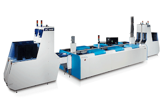
Depending on the capacity levels that are needed, SoLayTec offers three types of InPassion ALD. The main difference is the number of deposition units modules added in such a system. The basic three products offered are 4, 6 or 8 deposition units, which result in 2,400 wph, 3,600 wph or 4,500 wph respectively. (www.solaytec.com)
 
Fokko Pentinga, CEO and President of Amtech, commented, "This follow-on order brings the total ALD tools ordered by this specific customer to seven. Four systems have been put in production of PERC solar cells in the second half of fiscal 2017. The orders SoLayTec has received from this particular customer represent a total of 1GW of PERC production capacity. This follow-on order validates our customer's confidence in the performance capabilities of our spatial ALD system in high-volume production of PERC solar cells. There is a high level of enthusiasm in the PV marketplace for PERC solutions and this manufacturing platform supports our customers' goals to improve the total cost of ownership by increasing cell efficiency."

Thursday, December 14, 2017

Ultrahigh Elastic Strain Energy Storage in Metal-Oxide-Infiltrated Patterned Hybrid Polymer Nanocomposites

Phys.org reports: A team of scientists from the U.S. Department of Energy's Brookhaven National Laboratory and the University of Connecticut have developed a customizable nanomaterial that combines metallic strength with a foam-like ability to compress and spring back.
 
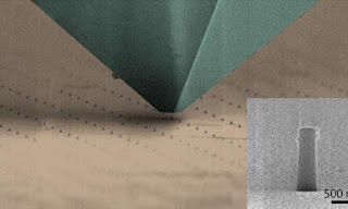
This scanning electron micrograph (SEM) image shows the nanomechanical testing tip passing over the arrays of custom-made nanopillars as it applies pressure to test elasticity and energy storage potential. The inset shows the structure of an individual hybrid nanopillar. Credit: Brookhaven National Laboratory

Read more at: https://phys.org/news/2017-12-scientists-nanoscale-pillars-memory-foam.html#jCp

This scanning electron micrograph (SEM) image shows the nanomechanical testing tip passing over the arrays of custom-made nanopillars as it applies pressure to test elasticity and energy storage potential. The inset shows the structure of an individual hybrid nanopillar. Credit: Brookhaven National Laboratory

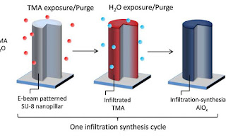
According to the supplemantary information The patterned SU-8 nanopillars were subjected to the AlOx infiltration synthesis at 85 °C using a commercial ALD system (Cambridge Nanotech Savannah S100). TMA (Sigma-Aldrich) was infiltrated into the polymer template for 5 min (vapor pressure <100 Torr), followed by N2 purging of the ALD chamber for 5 min (100 sccm). Then, water vapor was infiltrated into the polymer next for 5 min (pressure < 10 Torr), followed by N2 purging for 5 min, completing one synthesis cycle. A total of up to 16 cycles were applied.

This diagram shows the breakthrough synthesis process developed for these hybrid nanomaterials. First, electron-beam lithography carves the isolated nanopillars, then an aluminum vapor (TMA) infiltrates the pores in the structures, and finally exposure to water creates the final aluminum-oxide infused material. Credit: Brookhaven National Laboratory.

Please finde the abstract from Nanoletters below.
 
Read more at: LINK

Ultrahigh Elastic Strain Energy Storage in Metal-Oxide-Infiltrated Patterned Hybrid Polymer Nanocomposites

Nano Lett., 2017, 17 (12), pp 7416–7423
DOI: 10.1021/acs.nanolett.7b03238

Modulus of resilience, the measure of a material’s ability to store and release elastic strain energy, is critical for realizing advanced mechanical actuation technologies in micro/nanoelectromechanical systems. In general, engineering the modulus of resilience is difficult because it requires asymmetrically increasing yield strength and Young’s modulus against their mutual scaling behavior. This task becomes further challenging if it needs to be carried out at the nanometer scale. Here, we demonstrate organic–inorganic hybrid composite nanopillars with one of the highest modulus of resilience per density by utilizing vapor-phase aluminum oxide infiltration in lithographically patterned negative photoresist SU-8. In situ nanomechanical measurements reveal a metal-like high yield strength (∼500 MPa) with an unusually low, foam-like Young’s modulus (∼7 GPa), a unique pairing that yields ultrahigh modulus of resilience, reaching up to ∼24 MJ/m3 as well as exceptional modulus of resilience per density of ∼13.4 kJ/kg, surpassing those of most engineering materials. The hybrid polymer nanocomposite features lightweight, ultrahigh tunable modulus of resilience and versatile nanoscale lithographic patternability with potential for application as nanomechanical components which require ultrahigh mechanical resilience and strength.