Sunday, August 20, 2017

Atomic layer etching of MOCVD epitaxial gallium nitride

As have been reported before by Lund Nano Lab in Sweden (e.g. at ALE2016 Ireland and ALE2017 Denver) it is quite possible to use a standard ICP reactive ion etch chamber to run Atomic Layer Etching (ALE). Here is a nice publication from Aalto University in Finland and current and ex scientists from Lund Nano Lab in Sweden transferring the ALE processes from Lund and running it on an Oxford Instruments Plasmalab 100 in ALE mode etching GaN in Helsinki Micronova clean room.


The Oxford Instruments Plasmalab 100 at Aalto University Micronova clean room (LINK to technical specs and capabilities) 

MOCVD grown epitaxial AlGaN/GaN heterostructures implemented in high electron mobility transistors (HEMTs) have a well-defined layered structure with the two-dimensional electron gas (2DEG). However, etching of the gate recess is challenging as conventional RIE does not provide sufficiently good control over the etch process, and high energy ions can cause damage to the 2DEG layer. This paper showcase how these problems can be avoided if GaN ALE is used in etching these recesses.


Sabbir Khan - the ALE King tuning the Plasma at Lund Nano Lab.

Besides techniques of growing a single monolayer or few monolayers of GaN are challenging. GaN ALE could provide an alternative method to the 2D material community by a controlled thinning of high quality films of GaN down to a few atomic layers.

Please find the abstract to the Open Access JVSTA publication below:


Atomic layer etching of gallium nitride (0001)
Christoffer Kauppinen, Sabbir Ahmed Khan, Jonas Sundqvist, Dmitry B. Suyatin, Sami Suihkonen, Esko I. Kauppinen, and Markku Sopanen

Journal of Vacuum Science & Technology A: Vacuum, Surfaces, and Films 35, 060603 (2017); doi: http://dx.doi.org/10.1116/1.4993996


Abstract: In this work, atomic layer etching (ALE) of thin film Ga-polar GaN(0001) is reported in detail using sequential surface modification by Cl2 adsorption and removal of the modified surface layer by low energy Ar plasma exposure in a standard reactive ion etching system. The feasibility and reproducibility of the process are demonstrated by patterning GaN(0001) films by the ALE process using photoresist as an etch mask. The demonstrated ALE is deemed to be useful for the fabrication of nanoscale structures and high electron mobility transistors and expected to be adoptable for ALE of other materials.

Saturday, August 19, 2017

OSRAM Opto Semiconductor Acquires MOCVD Systems from AIXTRON

AIXTRON announced that OSRAM Opto Semiconductors has purchased the company's AIX 2800G4-TM Planetary system for the manufacturing of mainly infrared-based high power lasers and LEDs based on gallium arsenide (GaAs).

Source: LEDinside LINK
Photo credit: Aixtron (www.aixtron.com)
From Aixtron Press release: “We are very pleased that OSRAM Opto Semiconductors has selected our AIX 2800G4-TM platform for the production of high power laser and infrared LED devices. Their trust in our AIX 2800G4-TM system confirms our strategy to focus on solutions for the most demanding applications, where superior process performance is mandatory to meet our customer’s requirements. Following the recent qualification of our AIX G5 C platform and achieving this key milestone also with the AIX 2800G4-TM, we are looking forward to further deepen our partnership with one of the most innovative semiconductor manufacturers worldwide”, explains Dr. Frank Schulte, Vice President AIXTRON Europe.

Wednesday, August 16, 2017

Don´t miss any ALD News!

Here is a service provided by BALD Engineering that you can order your own personalized e-mail news service for the two News Blogs operated by BALD Engineering. The feed can also be integrated into any feed reader you may be using or if you like to provide the news feed on your website. You´re welcome to do so - it is for free! 

There is a obvious unsubscribe link at the beginning of each e-mail so when ever you´re feeling fully saturated just click on the link to unsubscribe ;-)

This is especially convenient for those of you in countries were LinkedIn is currently blocked, which is typically the way of getting the news otherwise. Just click on the links below and you can set it up as you like (two examples as screendumps below).

BALD News Blog: http://feeds.feedburner.com/AldNewsBlog-BaldEngineering

BALD Financials: http://feeds.feedburner.com/BaldFinancials


Monday, August 14, 2017

University of Helsinki present a thermal ALD gold process

Some years ago Barry Lab presented their plasma enhanced gold ALD process (LINK). However, in order to coat 3D features and objects plasma activated processes have limitations so that is why it is now very cool to read about a thermally activated ALD process for gold from University of Helsinki. They have identified a precursor, Me2Au(S2CNEt2), with a quite broad thermal ALD process window (120–250 °C). Amazingly, as for the earlier breakthrough from Helsinki on Ruthenium ALD, the trick is to use a oxygen co reactant and for gold the Finns had to go all the way and use ozone. Read all about the details in the paper below.

Thermal Atomic Layer Deposition of Continuous and Highly Conducting Gold Thin Films
Maarit Mäkelä, Timo Hatanpää, Kenichiro Mizohata, Jyrki Räisänen, Mikko Ritala, and Markku Leskel

Abstract:
Five Au(III) compounds were synthesized and evaluated for atomic layer deposition of Au thin films. One of the compounds, Me2Au(S2CNEt2), showed optimal thermal characteristics while being volatile and thermally stable. In the growth experiments, this compound was applied with O3 at temperatures of 120–250 °C. Self-limiting growth was confirmed at 180 °C with a rate of 0.9 Å/cycle. The deposited Au thin films were uniform, polycrystalline, continuous, and conductive. Typical resistivity values of 40 nm thick films were 4–16 μΩ cm, which are low for chemically deposited thin films. The chemical composition of a Au thin film deposited at 180 °C was analyzed by time-of-flight elastic recoil detection analysis, proving the film was pure with small amounts of impurities. The detected impurities were O (2.9 atom %), H (0.9 atom %), C (0.2 atom %), and N (0.2 atom %).

Friday, August 11, 2017

A new featherweight, flame-resistant and super-elastic metamaterial from Purdue Uniuversity

Purdue University reports: WEST LAFAYETTE, Ind. — A new featherweight, flame-resistant and super-elastic metamaterial has been shown to combine high strength with electrical conductivity and thermal insulation, suggesting potential applications from buildings to aerospace.


A new composite material combines ultra-lightweight with flame-resistance, super-elasticity and other attributes that could make it ideal for various applications. Here, the material is viewed with a scanning electron microscope, while its flame resistance is put to the test. (Purdue University photo)

[From the abstract, Adv. Mater., DOI: 10.1002/adma.201605506] "A ceramic/graphene metamaterial (GCM) with microstructure-derived superelasticity and structural robustness is achieved by designing hierarchical honeycomb microstructures, which are composited with two brittle constituents (graphene and ceramic) assembled in multi-nanolayer cellular walls. Attributed to the designed microstructure, well-interconnected scaffolds, chemically bonded interface, and coupled strengthening effect between the graphene framework and the nanolayers of the Al2O3 ceramic (NAC), the GCM demonstrates a sequence of multifunctional properties simultaneously that have not been reported for ceramics and ceramics–matrix–composite structures, such as flyweight density, 80% reversible compressibility, high fatigue resistance, high electrical conductivity, and excellent thermal-insulation/flame-retardant performance simultaneously."
 
Findings were detailed in a research paper published on May 29 in the journal Advanced Materials. The paper was a collaboration between Purdue, Lanzhou University and the Harbin Institute of Technology, both in China, and the U.S. Air Force Research Laboratory. A research highlight about the work appeared in the journal Nature Research Materials and is available at https://www.nature.com/articles/natrevmats201744.pdf. A YouTube video (below) about the work is available at https://youtu.be/PVd-eS_KMlU.

The ALD process of the nanolayer Al2O3 ceramic (NAC) were performed in an Utratech Fiji F200 (now Veeco CNT) ALD system at 250 °C using trimethylaluminum (TMA) and H2O.


Tuesday, August 8, 2017

New promising ALD catalyst for CO2 splitting

Scientists from École polytechnique fédérale de Lausanne (EPFL) in Switzerland has reported a low cost system to split carbon dioxide to carbon monoxide and oxygen using an ALD tin oxide catalyst on copper oxide nanowires. The devis is working at a rather efficiency of 13.4%, which opens up new paths to get rid of the man made CO2 that is currently heating up our planet and causing extreme weather conditions everywhere  - believe it or not.
The research comes out of the famous laboratory of Prof. Michael Grätzel at EPFL, one of the worlds top 10 most cited chemists and most certainly the most cited chemist from Dorfchemnitz in Saxony, Germany. One of his most famous invention is the so called Gräzel cell - a dye-sensitized solar cell, which is a low-cost version of thin film solar cells and he was awarded the 2010 Millennium Technology Prize for this invention.
Michael Grätzel (born 11 May 1944, in Dorfchemnitz, Saxony, Germany) is a professor at the École Polytechnique Fédérale de Lausanne where he directs the Laboratory of Photonics and Interfaces [Wikipedia].
Using Earth-abundant materials, EPFL scientists have built the first low-cost system for splitting CO2 into CO, a reaction necessary for turning renewable energy into fuel.

The future of clean energy depends on our ability to efficiently store energy from renewable sources and use it later. A popular way to do this is to electrolyze carbon dioxide to carbon monoxide, which is then mixed with hydrogen to produce liquid hydrocarbons like gasoline or kerosene that can be used as fuel. However, we currently lack efficient and Earth-abundant catalysts for the initial splitting of CO2 into CO and oxygen, which makes the move into expensive and prohibitive. EPFL scientists have now developed an Earth-abundant catalyst based on copper-oxide nanowires modified with . The system can split CO2 with an efficiency of 13.4%. The work is published in Nature Energy, and can help worldwide efforts to synthetically produce carbon-based fuels from CO2 and water.

Read more at: https://phys.org/news/2017-06-low-cost-carbon-dioxide.html#jCpv
Using Earth-abundant materials, EPFL scientists have built the first low-cost system for splitting CO2 into CO, a reaction necessary for turning renewable energy into fuel.

The future of clean energy depends on our ability to efficiently store energy from renewable sources and use it later. A popular way to do this is to electrolyze carbon dioxide to carbon monoxide, which is then mixed with hydrogen to produce liquid hydrocarbons like gasoline or kerosene that can be used as fuel. However, we currently lack efficient and Earth-abundant catalysts for the initial splitting of CO2 into CO and oxygen, which makes the move into expensive and prohibitive. EPFL scientists have now developed an Earth-abundant catalyst based on copper-oxide nanowires modified with . The system can split CO2 with an efficiency of 13.4%. The work is published in Nature Energy, and can help worldwide efforts to synthetically produce carbon-based fuels from CO2 and water.

Read more at: https://phys.org/news/2017-06-low-cost-carbon-dioxide.html#jCp

Below the abstract and the link to the Nature Energy publication

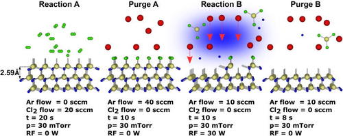
Solar conversion of CO2 to CO using Earth-abundant electrocatalysts prepared by atomic layer modification of CuO


Marcel Schreier, Florent Héroguel, Ludmilla Steier, Shahzada Ahmad, Jeremy S. Luterbacher, Matthew T. Mayer, Jingshan Luo & Michael Grätzel

Nature Energy 2, Article number: 17087 (2017) doi:10.1038/nenergy.2017.87

Abstract: The solar-driven electrochemical reduction of CO2 to fuels and chemicals provides a promising way for closing the anthropogenic carbon cycle. However, the lack of selective and Earth-abundant catalysts able to achieve the desired transformation reactions in an aqueous matrix presents a substantial impediment as of today. Here we introduce atomic layer deposition of SnO2 on CuO nanowires as a means for changing the wide product distribution of CuO-derived CO2 reduction electrocatalysts to yield predominantly CO. The activity of this catalyst towards oxygen evolution enables us to use it both as the cathode and anode for complete CO2 electrolysis. In the resulting device, the electrodes are separated by a bipolar membrane, allowing each half-reaction to run in its optimal electrolyte environment. Using a GaInP/GaInAs/Ge photovoltaic we achieve the solar-driven splitting of CO2 into CO and oxygen with a bifunctional, sustainable and all Earth-abundant system at an efficiency of 13.4%

Saturday, August 5, 2017

Gartner projects a strong year for Etch and CVD in 2017

Gartner Says Worldwide Semiconductor Capital Spending Is Forecast to Grow 10.2 Percent in 2017

(Gartner press release, August 2, 2017) Worldwide semiconductor capital spending is projected to increase 10.2 percent in 2017, to $77.7 billion, according to Gartner, Inc. This growth rate is up from the previous quarter's forecast of 1.4 percent, due to continued aggressive investment in memory and leading-edge logic which is driving spending in wafer-level equipment (see Table 1).

"Spending momentum is more concentrated in 2017 mainly due to strong manufacturing demand in memory and leading-edge logic. The NAND flash shortage was more pronounced in the first quarter of 2017 than the previous forecast, leading to over 20 percent growth of etch and chemical vapor deposition (CVD) segments [includes ALD] in 2017 with a strong capacity ramp-up for 3D NAND,"
said Takashi Ogawa, research vice president at Gartner.

According to Gartner's latest view, the next cyclical down cycle will emerge in 2018 to 2019 in capital spending, compared with 2019 to 2020 in the previous quarter's forecast. "Spending on wafer fab equipment will follow a similar cycle with a peak in 2018. While the most likely scenario will still keep positive growth in 2018, there is a concern that the growth will turn negative if the end-user demand in key electronics applications is weaker than expected," said Mr. Ogawa.

Worldwide Semiconductor Capital Spending and Equipment Spending Forecast, 2016-2020(Millions of Dollars)
 

Thursday, August 3, 2017

Coventor solutions to atomic level challenges in semiconductor technology

Atomic Level Processing technology like ALD and ALE are crucial for current and coming nodes in both logic and memory. So for you atomic level people it may be interesting to keep a close track of the current challenges and solutions  in scaling and patterning. Here are three interesting articles by Coventor covering this topics (from the Coventor August 2017 news letter).

What drives SADP BEOL variability (LINK)?


Figure from Coventor August 2017 newsletter


Until EUV lithography becomes a reality, multiple patterning technologies such as triple litho-etch (LELELE), self-aligned double patterning (SADP), and self-aligned quadruple patterning (SAQP) are being used to meet the stringent patterning demands of advanced back-end-of-line (BEOL) technologies. In this blog, we modeled SADP process variability to try to understand the effect of this variability on BEOL and RC performance.

How small variations in photoresist shape significantly impact multi-patterning yield (LINK)

 Figure from Coventor August 2017 newsletter
Things were easy for integrators when the pattern they had on the mask ended up being the pattern they wanted on the chip. Multi-patterning schemes such as Self-Aligned Double Patterning (SADP) and Self-Aligned Quadruple Patterning (SAQP) have changed that dramatically. In this blog, we look at how small variations in photoresist shape can significantly impact multi-patterning yield.

Problems and Solutions at 7nm (LINK)

As we approach 7nm and lower technology nodes, lithography, patterning, material and interconnect challenges abound. David Fried, Chief Technology Officer of Coventor, addresses these challenges in a video interview with Ed Sperling of Semiconductor Engineering. David also reviews the problems that we are facing at both 7nm and 5nm and proposes some potential solutions. 


Movie from Coventor August 2017 newsletter as released on Youtube from an interview with Ed Sperling of Semiconductor Engineering.

Challenges in 3D-NAND high volume manufacturing

Planar NAND was scaled and at the end limited by the cost of lithography, wheras 3D NAND scaling is enabled by advanced deposition and etch processes defining complex high aspect ratio 3D structures. Here is an excellent article by Lam Research in Solid State Technology on the challenges in 3D-NAND fabrication.

Solis State Technology : LINK

Screen capture from Solid State Technology online magazine (LINK)

Wednesday, August 2, 2017

Rene Deubler to Drive Commercialization of RASIRC Technology

San Diego, Calif – August 1, 2017–RASIRC today announced that Rene Deubler has joined the company as Director of Sales. Deubler brings to RASIRC a proven track record of exceptional sales growth with new technologies. His past experience includes engineering, program management, field service, and sales for both domestic and European semiconductor OEMs. His primary focus is growth of sales of RASIRC products including the Peroxidizer®, Hydrogen Peroxide Steamers, BRUTE® Peroxide and Hydrazine, and the RainMaker® Humidification System (RHS)
 
 
“I was attracted to RASIRC by its reputation for solving difficult problems in semiconductor processes and then converting those solutions to unique products,” said Deubler. “I look forward to expanding the reach of our equipment and chemistries into new markets.”

Deubler holds an MBA in Project Management from the Keller Graduate School of Management. He also holds a degree in Computer Science and Electrical Engineering from Höhere Technische Lehranstalt in Austria. Prior to RASIRC, Deubler was General Manager for Von Ardenne North America, where he opened the US operation and grew the business to $76 million over six years. Prior to Von Ardenne, he was regional field service supervisor for EV Group, where he increased project efficiency, improved product quality and accelerated customer satisfaction.

“RASIRC products are poised for explosive growth for the next nodes of semiconductor manufacturing driven by our ALD and Hydrogen Peroxide technologies,” said Jeffrey Spiegelman, RASIRC President and Founder. “Rene’s background and drive will be essential in executing our global sales and marketing strategy.”

HERALD ECI event on Early Career Development

HERALD & ECI

The HERALD – Hooking together European research activity in Atomic Layer Deposition – COST action (MP1402) aims to structure and integrate European research activity in atomic layer deposition (ALD), bringing together existing groups, promoting young scientists and reaching out to industry and the public. In 2016, a network was formed within HERALD for Early Career Investigators (ECIs) to promote the next generation of ALD scientists and help them to establish themselves as research leaders in the ALD community. Broadening out the COST definition of ECI, the network welcomes investigators from within a year of submitting their PhD dissertation to PhD +10 years - however, these are not strict limits.

Program

In collaboration with COST action HERALD, Ghent University will host the 2nd HERALD Early Career Investigators (ECIs) Network event, which will be held on August 28-29, 2017. The aim of this lunch-to-lunch meeting is to bring together members of the network and exchange ideas and experiences on the challenges that come with establishing ourselves as a (prospective) research group leader. We have also invited some successful and established leaders in the field who will share their experiences and give advices on how to build a successful career path to full research independency. The meeting will offer opportunities for networking and discussions among the network members and invited speakers.

Tuesday, August 1, 2017

ALD helps searching for traces of drugs and bomb-making components

BUFFALO, N.Y. — Scientists searching for traces of drugs, bomb-making components and other chemicals often shine light on the materials they’re analyzing.

This approach is known as spectroscopy, and it involves studying how light interacts with trace amounts of matter. 
 

The image above depicts a new device for surface enhanced infrared absorption spectroscopy. Infrared light (the white beams) is trapped by tiny gaps in the metal surface, where it can be used to detect trace amounts of matter. Credit: University at Buffalo.
 
One of the more effective types of spectroscopy is infrared absorption spectroscopy, which scientists use to sleuth out performance-enhancing drugs in blood samples and tiny particles of explosives in the air.

Wednesday, July 26, 2017

A cool Fab movie form Intels D1X Fab

For those of you who have the hots for 3D printing, additive manufacturing and Industry 4.0 check out the real stuff happening every day 24/7. Here is a cool Fab movie form Intels D1X Fab that is a new extension of their D1D factory at the Ronler Acres campus in Hillsboro, Oregon. D1D/D1X is where the company designs and manufactures all the latest technology nodes : 14nm, 10nm and 7nm technology.

 Screendump (youtube.com)

At 00:18 in the movie below you can spot an ASM A412 Large Batch Furnace on the left with its characteristic pale yellow and white panels and the black tinted doors and windows. Summer competition - What other tools can you spot? Any ALD machines?


ASM report strong order intake in ALD for 3D-NAND and Foundry in its 2Q 2017 report

For 2017, the leading ALD equipment manufacturer ASM International expect a clear improvement in the single wafer ALD market and they forecast the single wafer ALD market to reach a size of about USD 1.5 billion by 2020-2021. As a comparasion the ALD market as a whole was estimated to USD 1.4 to 1.5 billion in 2016 (Gartner, VLSI Research, TECHCET), including all segments (e.g. Semi, MEMS, PV, OLED and R&D).

ASM International N.V. (Euronext Amsterdam: ASM) today reports its second quarter 2017 operating results (unaudited) in accordance with IFRS. (LINK)

Investor presentation Q2 2017
  • New orders at €206 million were 1% above the Q1 2017 level and 29% above last year's Q2 level.
  • Net sales for the second quarter 2017 were €202 million, an increase of 40% compared to the previous quarter. Year-on-year net sales increased with 46%.
  • Net earnings of €132 million in the second quarter included a result of €84 million from the 5% sale and dilution of the ASMPT stake.
  • Normalized net earnings for the second quarter 2017 increased by €14 million compared to the first quarter 2017. Operating result increased to €38 million. The financing result included €11 million negative effects from currencies compared to €7 million negative effects in the first quarter. The result from investments decreased with €4 million due to the dilution of our stake in ASMPT. Moreover the ASMPT results in the first quarter included a one-off non-cash gain of €10 million related to the revaluation of the convertible bond.


Commenting on the results, Chuck del Prado, President and Chief Executive Officer of ASM International said: 

"In Q2 we realized sales of €202 million, which was slightly above our guidance and at a historical high quarterly level. The order intake for Q2, at €206 million, came in at the high end of the forecast and was also at the highest level in the company's history. Order intake in ALD was primarily strong from the 3D-NAND and Foundry segments. We also received several Intrepid Epitaxy orders in Q2."


OUTLOOK
Based on our current assessment, we continue to expect a clear year-on-year improvement in the single wafer ALD market in 2017, with demand in the Logic/Foundry segment remaining healthy and a strong increase in the 3D-NAND segment.

For Q3 we expect a sales level of €170-190 million, on a currency comparable level, while for the second half of 2017 as a whole we expect a sales level higher than in the first half of 2017. After the very strong orders in the past two quarters we expect order intake in Q3 at a still healthy level of €150-170 million, on a currency comparable level.

Saturday, July 22, 2017

Veeco CNT ships its 500th ALD system

As reported by Solid State Technology: Veeco Instruments (Veeco) recently announced that Veeco CNT—formerly known as Ultratech/Cambridge Nanotech—shipped its 500th Atomic Layer Deposition (ALD) system to the North Carolina State University. The Veeco CNT Fiji G2 ALD system will enable the University to perform research for next-generation electronic devices including wearables and sensors. Veeco announced the overall acquisition of Ultratech on May 26 of this year. Executive technologists from Veeco discussed the evolution of ALD technology with Solid State Technology in an exclusive interview just prior to SEMICON West 2017.

Please find the article and interview by Ed Korczynski here (LINK)

Evolution of Atomic-Layer Deposition (ALD) technology starts with single-wafer thermal chambers, adds plasma energy, and then goes to batch processing for manufacturing. (Source: Veeco CNT, used with permision).


Friday, July 21, 2017

Join the Critical Materials Council (CMC) Conference 2018, April 26-27 in Phoenix

Join the Critical Materials Council (CMC) Conference 2018, April 26-27 in Phoenix, Arizona. Get actionable information on materials and supply-chains for current and future semiconductor manufacturing. 


Hotel location TBD

More details will be available soon on cmcfabs.org

For information on sponsorship please contact cmcinfo@techcet.com


Monday, July 17, 2017

Introducing the FlexAL-2D the ALD Plasma Processing System for 2D Materials

Oxford Instruments’ ALD and 2D technical specialists have teamed up with Eindhoven University of Technology research teams to develop the innovative FlexAL-2D for atomic layer deposition (ALD) of 2D transition metal dichalcogenides for nanodevice applications.

Source: AZoNano LINK

More information can also be found at http://www.oxinst.com/FlexAL2D
 

Saturday, July 15, 2017

RASIRC Releases Next Generation RainMaker Humidification System for Fine Water Vapor Delivery

RHS Solves ALD delivery problems by eliminating particles and microdroplets at very high or very low flow rates


San Diego, Calif – July 15, 2017–RASIRC today announced the release of the next generation RainMaker® Humidification System (RHS). The system incorporates a new control system that provides highly accurate, droplet free water vapor for advanced atomic layer deposition (ALD) processes. The RHS has a wide mass delivery range of 50 - 5100 mg/min water mass flow rate in carrier gases. The system is capable of highly accurate and precise delivery of gaseous water into pressures from atmosphere to high vacuum.

“As demands for film quality and uniformity in ALD/ALE processes become increasingly challenging, process engineers have reached the limits with bubbler delivery methods,” said Jeffrey Spiegelman, President and Founder of RASIRC. “The RHS solves problems associated with process control and microdroplet formation, leading to better film uniformity and fewer defects.”

 
The next generation RainMaker® Humidification System (RHS)
 

Thursday, July 13, 2017

On the road to Denver for ALD2017?

Twitter is heating up with announcements of people and companies going to the ALD2017 conference in Denver 15 to 18 of July. Here is a selection of some of them. Please take a chance to download the conference app (see tweet below)


Film Sense and Kurt J. Lesker: in-situ Ellipsometry with the FS-1

The Film Sense vision “to create easy-to-use and affordable ellipsometers” is especially relevant for in-situ applications. The Film Sense FS-1 realizes this vision by providing the power of Multi-Wavelength Ellipsometry, at an affordable price and compact size that is ideal for in-situ measurements. The FS-1 can provide real time thickness data with exceptional precision, which can be indispensable for the efficient development of new ALD processes. In the plot below, the “steps” in the data are direct observations of the thickness changes on the sample throughout the ALD cycles: the thickness increases and saturates as the precursor is introduced (trimethyl aluminum in this case), and then decreases as the film is oxidized (thermally by H2O in this case). 


The relationship between Film Sense and Kurt J. Lesker dates back to almost the inception of Film Sense.  In fact, the first Film Sense FS-1 in-situ testing was performed on a Kurt J. Lesker ALD150LX reactor in 2014.  The FS-1 has since been integrated on multiple Lesker ALD reactors, and has been used to characterize a wide variety of thin films including:  Al2O3, TiO2, HfO2, and TiN.

 
The ALD150LX was designed from the ground up for advanced R&D and features remote plasma as well as in-situ ellipsometry as a primary means of real time process monitoring and control during ALD.  Patented Precursor Focusing TechnologyTM (PFTTM) prevents unwanted film deposition on sensitive surfaces inside the reactor including the analytical port windows used for light transmission during in-situ ellipsometry.  The layout of the plasma-enhanced ALD (PEALD) reactor makes installation and operation of the compact FS-1 unit simple and easy. 

According to Bruce Rayner, Principal Scientist – ALD at the Kurt J. Lesker Company, “The FS-1 provides excellent performance at a very attractive price, and its robust, compact design is ideally suited for in-situ ALD applications.”

If you are coming to ALD2017 in Denver, please visit the Lesker booth #31 to see a live demonstration of the FS-1 integrated on an ALD150LX reactor.  At the Film Sense booth #1, an FS-XY150 automated mapping stage will be on display.

The Film Sense FS-1 ellipsometer is now available as an option for the Lesker ALD150LX reactor.  For more information please contact Dan Hadwiger (mailto:dhadwiger@film-sense.com) or Noel O’Toole (mailto: noelo@lesker.com), or visit our websites at http://www.film-sense.com/products/fs-1-ald-applications/fs-1-lesker-ald150lx and https://www.lesker.com/newweb/vacuum_systems/deposition_systems_ald_ald150lx.cfm.