Wednesday, December 14, 2016

Grow Low Temperature Nitrides by Atomic Layer Deposition Without Plasma


Unique Hydrazine formulation and package enables HAR and 3D film studies for Laboratories


At ALD Lab Saxony we have excellent previous experience with employing the RASIRC technology for dry hydrogen peroxide delivery in High-k ALD processes for PV and Logic applications. That is why we are very happy to announce that RASIRC from San Diego, California will be sponsoring, attending and exhibiting at ALD for Industry 17-18th of January in Dresden Germany. This is an excellent opportunity to meet RASIRC and learn about their latest product release for safe and effective delivery of hydrazine for Atomic Level Processing. Please find the product fact sheet below.

RASIRC BRUTE® Hydrazine - Laboratory Version is specifically designed for universities and research institutes in development of Atomic Layer Deposition and Etch (ALD and ALE) processes with compressed thermal budgets. Hydrazine molecules can enable low temperature metal nitridation, opening up many potential avenues for advancements in High Aspect Ratio (HAR) and three dimensional structures grown via ALD and ALE.

“This new vaporizer package should enable researchers to investigate low temperature thermal nitride processes without a large budget.” - Jeff Spiegelman President and CEO of RASIRC.


Scientists working with TiNx, TaNx, SiNx, WNx, Platinum, Palladium, Cobalt or other new materials can benefit from using BRUTE Hydrazine. Additional benefits may be found from the generation of radical hydrogen and limited etching and surface cleaning effects. 


Figure 1: BRUTE Hydrazine (50ml). Based on RASIRC Drawing #202268

BRUTE Hydrazine delivers water-free hydrazine gas (N2H4) to process in a controlled, repeatable manner. Preloaded in a non-volatile solvent, the Brute Hydrazine chemistry is packaged in a single use vaporizer (Figure 1) with metal seals, making hydrazine gas simple to connect and deliver. 

Benefits of the Laboratory Version 

  • Sized for universities and research labs
  • Improved safety—RASIRC patent pending solvent delivery system raises the flash point
  • Simple plug-and-play design with a single connection to the vaporizer
  • Direct vacuum draw
  • Manual operation
  • Less chemistry than industrial ampoules, improving safety
  • Low cost
  • Smaller footprint

BRUTE Hydrazine Applications

BRUTE Hydrazine can be used for a wide range of low temperature processes including ALD, ALE, MOCVD and nitride materials development:
  • Contact barrier and other memory applications using TiN and TaNx
  • Precursor for TiN gate stack and other transistor applications
  • Sidewall spacer/etch stop (SiNx) between metals and silicon or dielectric materials
  • Multiple patterning involving SiO2 and SiNx
  • Selective deposition and etch involving metal nitrides and SiO2
  • SiGe passivation involving SiNx, SiOxNy and BN
  • Metal nitride deposition (WNx)
  • Low temperature metal oxide reduction for metal ALD (Co, Cu, Pd, Pt)
  • Atomic removal of surface carbon

Enables New Material

Plasma and ammonia-based methods fail to meet next generation process requirements for lower thermal budgets and ability to act deep within high aspect ratio or 3D structures.
  • Plasma cannot uniformly coat the sidewalls of high aspect ratio structures and can cause surface damage
  • Ammonia (NH3) has limited reactivity at low process temperatures, which leads to poor film quality
  • Standard High Purity Hydrazine has measurable water that leads to oxygen incorporation in nitride films increasing film resistance
BRUTE Hydrazine solves these problems. 


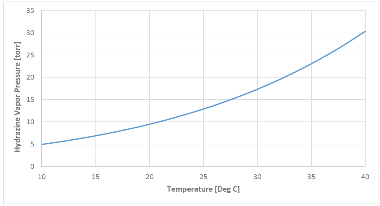
Figure 2: Theoretical Vapor Pressure Curve of BRUTE Hydrazine

BRUTE Hydrazine Characteristics

  • Dry (less than 50 ppm H2O in the liquid source), resulting in minimal oxygen contamination
  • Higher reactivity than NH3, enabling lower temperature ALD applications (200-400°C)
  • Better penetration of high aspect ratio structures, creating uniform films

How it Works

BRUTE Hydrazine provides a stable, reliable flow of anhydrous hydrazine gas from a liquid source in a metal sealed vaporizer (Figure 1). The liquid source combines anhydrous hydrazine and a proprietary non-volatile solvent, significantly increasing the flashpoint. This makes the chemistry safer to handle than anhydrous hydrazine. To deliver hydrazine gas to process, vacuum is applied to the BRUTE Hydrazine vaporizer to evaporate liquid BRUTE Hydrazine to pure hydrazine, leaving the non-volatile solvent behind. The Theoretical Vapor Pressure Curve of BRUTE Hydrazine is given in Figure 2.

How to Order

To place an order for 50ml BRUTE Hydrazine contact RASIRC at sales@rasirc.com and order P/N: 100784.

 
RASIRC specializes in products that generate and deliver gas to fabrication processes. Each unit is a dynamic gas plant in a box - converting common liquid chemistries into safer and more reliable gas flow for most processes. First to generate ultra-high purity (UHP) steam from de-ionized water, RASIRC technology can now also deliver hydrogen peroxide gas and hydrazine gas in controlled, repeatable concentrations. RASIRC gas delivery systems, humidifiers, and closed loop humidification systems are critical for many applications in semiconductor, photovoltaic, pharmaceutical, medical, biological, fuel cell, and power industries. 

Tuesday, December 13, 2016

Semiconductor Equipment Sales Forecast ─ $40 Billion

TOKYO — December 13, 2016 — SEMI, the global industry association representing more than 2,000 companies in the electronics manufacturing supply chain, today reported that worldwide sales of new semiconductor manufacturing equipment are projected to increase 8.7 percent to $39.7 billion in 2016, according to the SEMI Year-end Forecast, released today at the annual SEMICON Japan exposition. In 2017, another 9.3 percent growth is expected, resulting in a global semiconductor equipment market totaling $43.4 billion.


The SEMI Year-end Forecast predicts that wafer processing equipment, the largest product segment by dollar value, is anticipated to increase 8.2 percent in 2016 to total $31.2 billion. The assembly and packaging equipment segment is projected to grow by 14.6 percent to $2.9 billion in 2016 while semiconductor test equipment is forecast to increase by 16.0 percent, to a total of $3.9 billion this year.

For 2016, Taiwan and South Korea are projected to remain the largest spending regions, with China joining the top three for the first time. Rest of World (essentially Southeast Asia), will lead in growth with 87.7 percent, followed by China at 36.6 percent and Taiwan at 16.8 percent.

SEMI forecasts that in 2017, equipment sales in Europe will climb the most, 51.7 percent, to a total of $2.8 billion, following a 10.0 percent contraction in 2016. In 2017, Taiwan, Korea and China are forecast to remain the top three markets, with Taiwan maintaining the top spot even with a 9.2 percent decline to total $10.2 billion. Equipment sales to Korea are forecast at $9.7 billion, while equipment sales to China are expected to reach $7.0 billion.

The following results are given in terms of market size in billions of U.S. dollars:

Monday, December 12, 2016

ALD of High-k using molecular oxygen at Stanford Nanofabrication Facility

The Stanford Nanofabrication Facility (SNF) is administarting a fantastic Wiki for their clean room equipment and processeses in nanofabrication. The Wiki is there for the SNF lab community as a resource and also as historical archive as stated in the Wiki description. For all us not part of SNF it is nice that a login is not needed to view public information available.

In the wiki you will find vast process archives for the tools operated and for us ALD people the ALD section is especially interesting to study. As listed SNF is operating 4 ALD Tools all from Ultratech CNT : one Savannah and three Fiji´s.

SNF ALD Wiki  : LINK

SNF list of available films : LINK

Recently SNF published a great review of their metal alkyl amide High-k PEALD processes and the good news is that it is open source easily available for all of us to study.
 

Atomic layer deposition by reaction of molecular oxygen with tetrakisdimethylamido-metal precursor

J Provine, Peter Schindler, Jan Torgersen, Hyo Jin Kim, Hans-Peter Karnthaler and Fritz B. Prinz

J. Vac. Sci. Technol. A 34, 01A138 (2016); http://dx.doi.org/10.1116/1.4937991

Wednesday, December 7, 2016

Ultrathin protective ALD layer brings more stability to perovskite solar cell

TU Eindhoven reports: The addition of a few nanometers of a thin layer of aluminum oxide protects a perovskite solar cell against humidity – still a major stumbling block to the commercial application of this new type of solar cell. A surprising bonus is a yield boost of 3 percent. These are the findings of researchers at Eindhoven University of Technology and research institute ECN, part of the Solliance collective, published today in the journal Energy and Environmental Science.

Solar cells made from perovskite have undergone rapid development in recent years. Perovskite is a mineral that has the same crystal structure as calcium-titanium-oxide (CaTiO3). The yield of this type of solar cell has risen to 22% in just a few years. A drawback for the moment, though, is the damaging effect of humidity: water vapor from the atmosphere reacts with the perovskite crystals causing a considerable reduction in the yield over time. This instability is a stumbling block to successful commercialization.
“Although Al2O3 has electrically insulating properties, it can still be used as a buffer layer between the semi-conductive perovskite and the conductive contacts by limiting the thickness of the layer to one nanometer or less,” says FOM PhD student and first author Dibyashree Koushik (TU/e group Plasma and Materials Processing). 

Full story at TU Eindhoven : LINK

High-Efficiency Humidity-Stable Planar Perovskite Solar Cells Based On Atomic Layer Architecture

D. Koushik, W.J.H. Verhees, Y. Kuang, S. Veenstra, D. Zhang, M.A. Verheijen, M. Creatore, and R.E.I. Schropp, Energy and Environmental Science (5 december 2016). The study was co-funded by the FOM Foundation

Tuesday, December 6, 2016

Joint EuroCVD-Baltic ALD 2017: Abstract submission open!

The abstract submission for the Joint EuroCVD-BalticALD conference in Linköping, Sweden 11-14 June 2017 is now open.
 
Abstract deadline is 10 January 2017

Topics for this conference include:  
  • Precursors (design, synthesis and delivery)
  • Modelling (surface, gas phase, thermo chemistry, quantum chemistry, multi scale)
  • Process Equipment (reactors)
  • Energy Enhanced processes (Plasma, Hot wire, Photon)
  • Nanomaterials (particles, 2D-materials, nano structures)
  • In-situ monitoring (QCM, Ellipsometry, IR, syncrotron)
  • Oxides (TCO, high-k, hard coatings, thermal barriers)
  • Nitrides (semiconductors, conductors, hard coatings)
  • Carbides (hard coatings, semiconductors)Elemental films (metals, amorphous carbon)Emerging materials (hybrid MLD/ALD, sulfides)


UC Berkeley invest in Ultratech CNT Plasma ALD for Ferroelectric High-k materials research

SAN JOSE, Calif., Dec. 6, 2016 /PRNewswire/ -- Ultratech, Inc. (Nasdaq: UTEK), a leading supplier of lithography, laser-processing and inspection systems used to manufacture semiconductor devices and high-brightness LEDs (HB-LEDs), as well as atomic layer deposition (ALD) systems, today announced that the Laboratory for Emerging and Exploratory Devices (LEED), led by Professor Sayeef Salahuddin, Ph.D. of the Electrical Engineering and Computer Sciences Department at UC Berkeley (EECS UC Berkeley), has chosen the Ultratech-CNT Fiji G2 PEALD system as its instrument of choice for its research activities. Professor Salahuddin was recently honored at the White House by President Barack Obama for his work in developing nano-scale electronic and spintronic devices for low power logic and memory applications.

"ALD provides an exciting way of accessing ferroelectric materials, which play a key role in these types of devices, by providing a means of controlling the film properties through the precise engineering of the composition," noted Professor Salahuddin. "This has led the way for us to explore the ferroelectric properties of metal oxides, such as Hafnium oxide, by adding a variety of dopants, such as silicon (Si), aluminum (Al), and yttrium (Y). Our decision in choosing the Fiji system was motivated not only by the system's performance, and flexibility but also because of the strong reputation that the Ultratech ALD team has for R&D expertise, coupled with its excellent support."

Adam Bertuch, senior thin film scientist at Ultratech-CNT, who has played a key role in the development of PEALD oxides at the company, said, "The Fiji is an extremely versatile instrument, which has been at the leading edge of the development of complex materials. Professor Salahuddin's work in the field of ferroelectric materials speaks for itself, and we are looking forward to having a strong collaborative relationship with him, as well as his scientific group at UC Berkeley."

The Fiji series is a modular, high-vacuum ALD system that accommodates a wide range of deposition modes using a flexible architecture and multiple configurations of precursors and plasma gases. The result is a next-generation ALD system capable of performing thermal and plasma-enhanced deposition (LINK).

Ultratech Fiji G2 ALD System

For advanced thin films, the Fiji series is a modular, high-vacuum ALD system that accommodates a wide range of deposition modes using a flexible architecture and multiple configurations of precursors and plasma gases. The result is a next-generation ALD system capable of performing thermal and plasma-enhanced deposition. Ultratech CNT has applied advanced computational fluid dynamics analyses to optimize the Fiji reactor, heaters, and vapor trap geometries. The system's intuitive interface makes it easy to monitor and change recipes and processes as required. The Fiji is available in several different configurations, with up to six heated precursor ports that can accommodate solid, liquid or gas precursors, and up to six plasma gas lines. Options include a built-in ozone generator, Load Lock as well as several in-situ analysis tools, which offer significant experimental flexibility in a compact and affordable footprint.

Ferroelectric HfO2 at IEDM 2016

Ferroelectric HfO2 was a hot topic today Tuesday at IEDM. At 10:45 AM - A 28nm HKMG Super Low Power Embedded NVM Technology Based on Ferroelectric FETs was presented by Globalfoundries, NaMLab and Fraunhofer.


Figure form the IEDM abstract shared on LinkedIn by Prof. Thomas Mikolajick, Scientific Director at NaMLab gGmbH, Dreden, Germany.
 

Sunday, December 4, 2016

The Critical Materials Council (CMC) Celebrates 1st Anniversary

Please Join Us in Celebrating the 1st Anniversary of the Critical Materials Council as an integral part of TECHCET, formally with SEMATECH. 
 
A big "Thank you" to the original CMC members for their continued support!  


Over the course of this year, new members have been added to the CMC, including Intel, Micron, Samsung, and Broadcom. In 2017, we expect to have an even wider international presence.

In celebration, we are offering special discounts to material suppliers and fabs on CMC Membership, proceedings from the Shanghai CMC Seminar (just completed), as well as the ICPT Summaries/Proceedings. For more information, please contact Meena Sher at msher@techcet.com or go to www.cmcfabs.org/seminar

International Conference on Planarization/CMP Technology (ICPT): Beijing 2016
 
TECHCET brings directly to you a package of critical information from ICPT Beijing 2016 in the form of executive summaries on the entire event. Authored by Paul Feeney, recognized CMP veteran and technologist, the package includes a set of slides outlining the highlights of every keynote, invited, and oral talk, a hardcover copy of the proceedings, and a soft copy of the proceedings. To obtain your package for $399, please contact Meena Sher at msher@techcet.com. Please also ask about the option to have a Live Presentation and Q&A from our technologist, Paul Feeney.
 
ICPT is the world's largest conference dedicated to Planarization topics. 365 people registered to observe 117 keynote, invited, oral, and poster papers. 

 CMC Associate Membership Includes:
 
  • Critical Materials Report of your choosing, including updates throughout the year.
  • Meetings with Analysts
  • Unique Networking Opportunities!
    CMC Conference 2016
  • Discounts on CMC Conference registration
  • Ability to collectively work on issues of common concern (with CMC direction)
  • Opportunity to actively address CMC hot topics
  • ...and more!
 
Call Us For More Information! 
1-480-382-8336 ex. 101

Save The Date - 2nd Annual Critical Materials Conference May 11-12, 2017, in Dallas Texas

Save the Date for our 2nd Annual Critical Materials Conference in Dallas, Texas. Please visit our Seminars page to view the highlights from 2016. Call for Papers Starts Nov. 15.


  • Event Start Date: May 11, 2017
  • Event End Date:May 12, 2017
  • Event Venue: Dallas, Texas, USA

The Critical Materials Council is a membership-based organization collectively working toward anticipating, and solving Critical Materials Issues in a non-competitive environment by identifying/alleviating supply problems, sharing best practices, and working on industry standards for the benefit of the semi device fabrication community.


 Become a part of the Critical Materials Ecosystem!

  • Unique Networking and Active Collaboration Opportunities
  • Gain access to the latest customized supply chain news and analyst commentary
  • Receive an expertly-written Critical Materials Report Advisory of your choosing

Saturday, December 3, 2016

Russian and Finnish scientists fabricate ZnO ALD coated SWCNTs p-type field effect transistors

TASS reports: Russian scientists create carbon nanotubes coated with zinc oxide 

Researchers from Skoltech, Aalto University, and Peter the Great St. Petersburg Polytechnic University have successfully demonstrated the technique of coating zinc oxide on the surface of single-walled carbon nanotubes, the SPbPU’s press-service said. Based on the new material, ambipolar field transistors have been maintained which may find their applications in logic circuits and memory cells.

Please find the abstract below to a joint publication in Nanotechnology.


More:
http://tass.com/science/916385

Single-walled carbon nanotubes coated with ZnO by atomic layer deposition

, , , , , , , , , and

Nanotechnology, Volume 27,Number 48 

http://dx.doi.org/10.1088/0957-4484/27/48/485709

The possibility of ZnO deposition on the surface of single-walled carbon nanotubes (SWCNTs) with the help of an atomic layer deposition (ALD) technique was successfully demonstrated. The utilization of pristine SWCNTs as a support resulted in a non-uniform deposition of ZnO in the form of nanoparticles. To achieve uniform ZnO coating, the SWCNTs first needed to be functionalized by treating the samples in a controlled ozone atmosphere. The uniformly ZnO coated SWCNTs were used to fabricate UV sensing devices. An UV irradiation of the ZnO coated samples turned them from hydrophobic to hydrophilic behaviour. Furthermore, thin films of the ZnO coated SWCNTs allowed us switch p-type field effect transistors made of pristine SWCNTs to have ambipolar characteristics.

Friday, December 2, 2016

New Book - Growth and Transport in Nanostructured Materials (PVD, CVD & ALD)

Here is a good Christmas gift for the scientist you really care about.

Growth and Transport in Nanostructured Materials

Reactive Transport in PVD, CVD, and ALD

Authors: Angel Yanguas-Gil, Northwestern-Argonne Inst. of Science and Engineering, Northwestern University, Evanston, Illinois, USA 


This book will address the application of gas phase thin film methods, including techniques such as evaporation, sputtering, CVD, and ALD to the synthesis of materials on nanostructured and high aspect-ratio high surface area materials. We have chosen to introduce these topics and the different application fields from a chronological perspective: we start with the early concepts of step coverage and later conformality in semiconductor manufacturing, and how later on the range of application branched out to include others such as energy storage, catalysis, and more broadly nanomaterials synthesis. [Continue at Springer]

ASM International technical luncheon seminar in San Francisco at IEDM 2017, December 7

ASM International N.V. (Euronext Amsterdam: ASM) today announces that it will host a technical luncheon seminar in San Francisco, CA, US, on Wednesday, December 7, 2016, the third day of the IEDM Conference.


At this technology seminar ASM will highlight the challenges and potential solutions for achieving next generation 3D devices.

The agenda is as follows:

11:30 am Food and drinks

12:00 - 12:05 pm Ivo Raaijmakers (ASM) - Welcome and introduction

12:05 - 12:30 pm Invited speaker: Raghuveer Makala (SanDisk/WDC) - "Thin film deposition
challenges for 3D NAND"

12:30 - 12:55 pm Invited speaker: Jorge Kittl (Samsung) - "Perspectives on logic scaling and
implications for process requirements"

Following the presentations, there is an opportunity for open discussion and networking until 1:15 pm.

The ASM technology seminar will take place in the Golden Gate room (25th floor) at the Nikko Hotel (across from the Hilton San Francisco), San Francisco, CA 94102. The room will open at 11:30 am for invited attendees. Interested parties should contact Rosanne de Vries, +31 88 100 8569, rosanne.de.vries@asm.com.

President Obama set to block Aixtron sale

Seeking Alpha reports that President Obama is poised to block a Chinese company from buying Germany's Aixtron (NASDAQ:AIXG) because Northrop Grumman (NYSE:NOC), a major U.S. defense contractor, is among the chip equipment maker's customers.

It would mark only the third time in more than a quarter century that the White House rejected an investment by an overseas buyer as a national security risk.

Aixtron shares -6.5% in Frankfurt.


China Warns U.S. Against Blocking Aixtron Takeover

Aixtron shares fall amid U.S. national security concerns over acquisition by China’s Fujian Grand Chip Investment Fund [Wall Street Journal]

Obama bars China's Fujian from buying Aixtron's US business


The headquarters of German chip equipment maker Aixtron SE is pictured ... The Treasury Department said Obama was blocking the deal .. [Reuters]

Warum redet Amerika in der Aixtron-Übernahme mit?

Die Übernahme des deutschen Maschinenbauers Aixtron durch einen chinesischen Investor ruft die große Politik in Washi [FAZ - Frankfurter Allgemeine Zeitung]