Wednesday, August 31, 2016

NCD to deliver Lucida GD series ALD system for OLED encapsulation with Chinese display manufacturer, TIANMA

NCD reports today (8/31 2016) :The OLED market is going to prospect fast gigantic growing in the near future because OLED has the possibilities of bending, folding and various forms like circle, therefore it will be applied for flexible and wearable devices. Flexible OLEDs need excellent thin encapsulation layers in order to keep the property from the permeation of water and oxygen under the external environment using repeated bending, folding and rolling of devices. However, the current encapsulation based on PECVD is not satisfied with future flexible OLEDs, so new encapsulation technology would absolutely be required.

Many OLED manufactures are currently reviewing to use ALD technology because of obtaining the highest property from the encapsulation layers of OLED, but they have not been solving the low throughput and particle issues followed by using their ALD systems.

In order to clear these problems, NCD has completed to develop the 6th ALD equipment for thin film encapsulation which satisfies high quality, large area and high throughput applying for the inventive ALD technology, and we have been also continuously testing customer’s samples. NCD’s ALD encapsulation layer shows much better properties than that of PECVD, and the encapsulation capability on application for foldable products has been confirmed from the customers. As a result, NCD has recently entered into the contract with Chinese display manufacturer, TIANMA to supply the 5.5th generation class ALD system of Lucida GD series for thin film encapsulation of OLED. It apparently shows that NCD’s core technologies and the result of developments have been approved by the oversea customer.

NCD will keep doing our best to set Lucida GD series as the standard of all of flexible OLED encapsulation equipment with this achievement and become the number one global ALD Company with the best competitiveness making new challenges and developments.

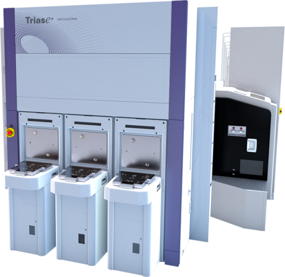
Lucida™ GD Series ALD


High throughput atomic layer deposition system for OLED displays 


Cluster system for Lucida™ GD series


Applications

  • Barrier layer(Al2O3, TiO2) for flexible substrate
  • WVTR(water vapor transmission rate) 5.3x10⁻⁵g/m2·day (tritiated water test @30nm Al2O3/PEN substrate)
  • Encapsulation layer(Al2O3,TiO2) for OLED
  • Applications of mass-product

Benefits

  • High throughput : > 30 panels/hour
  • Substrate size : > 6G (1500 x 1850mm2)

Features

  • Advanced process kit and small volume chamber for short gas cycle times
  • Extremely materialize ALD mechanism
  • Small foot print
  • Totally integrated process module
  • Easy process control

Technical specifications


Tuesday, August 30, 2016

Ultra-High Aspect Ratio InP Junctionless FinFETs by a Novel Wet Etching Method

Readers of this blog may have noticed that I got a new hobby and that I´ve been looking into some etching (ALE) on the side. Here is some interesting new results in etching InP Fins for future CMOS by a chemical method "enabled by inverse metal-assisted chemical etching". All recently published by University of Illinois researchers in Silicon Semiconductors and in the IEEE ElectronDevice Letter below. (Thanks Nicklas Nilsson for sharing this one).

A cross-sectional microscope image of a fin transistor. The indium phosphide semiconductor fin is overlaid with insulators and metals to make a working transistor. Image by Yi Song (as published in Silicon Semiconductors)

Ultra-High Aspect Ratio InP Junctionless FinFETs by a Novel Wet Etching Method

Yi Song et al
IEEE Electron Device Letters > Volume: 37 Issue: 8 

Abstract:
Junctionless FinFETs with an array of ultra-high aspect ratio (HAR) fins, enabled by inverse metal-assisted chemical etching, are developed to achieve high on-current per fin. The novel device fabrication process eliminates dry etching-induced plasma damage, high energy ion implantation damage, and subsequent high-temperature annealing thermal budget, ensuring interface quality between the high-k gate dielectric and the HAR fin channel. Indium phosphide junctionless FinFETs, of record HAR (as high as 50:1) fins, are demonstrated for the first time with excellent subthreshold slope (63 mV/dec) and ON/OFF ratio (3 × 10⁵). Published in: IEEE Electron Device Letters ( Volume: 37, Issue: 8, Aug. 2016 )

Picosun joins A*STAR Cost-Effective Interposer Consortim in Singapore

ESPOO, Finland, 30th August, 2016 – Picosun Oy, the leading supplier of advanced Atomic Layer Deposition (ALD) manufacturing solutions, partners with A*STAR’s Institute of Microelectronics (IME) in Singapore and global, prominent semiconductor industries to develop next generation chip packaging technology. 


A*STAR 2.5D interposer Multi-Project Wafer supported by state-of-the-art Through-Silicon Via (TSV) engineering lines in both 200mm and 300mm [A*STAR]
 
Higher and higher performance, speed, multifunctionality, reliability, and compact size are required from today’s microelectronics, to answer the customers’ demands, while the manufacturing costs must remain low to retain competitiveness.

The Cost-Effective Interposer Consortium brings together frontline semiconductor manufacturers and research institutes to address these challenges. Picosun joins forces with e.g. IME, Inotera Memories, STATS ChipPAC Pte. Ltd., Teradyne Corporation, Tessolve Semiconductor Pvt. Ltd., UMC, and Veeco Instruments to develop advanced, high volume manufacturing solutions for cost-efficient packaging of the chip components.

“We are happy to have Picosun as a member in the Cost-Effective Interposer Consortium. This collaborative partnership will harness the expertise of our partners, including Picosun’s strong know-how in ALD, and IME’s deep R&D experience to accelerate the development and time-to-market of cost-efficient next-generation electronic devices,” says Prof. Dim-Lee Kwong, Executive Director of IME.

“ALD is a central manufacturing method in today’s semiconductor industries, and the very technology that enables the future developments in the field. For Picosun, this is clearly our most important market area, where several world-leading IC industries already rely on our production-proven ALD solutions. We are excited to collaborate with such a number of prominent microelectronics industries and our long-time partner and valued customer, IME, in the Cost-Effective Interposer Consortium,” states Juhana Kostamo, Managing Director of Picosun.

A central approach to solve many key challenges in modern microelectronics development is wafer-level 3D-integration of the components, which enables continued downscaling of the chip size while retaining high performance and reliability. Cost savings are obtained when larger number of chips can be manufactured on the same wafer. ALD is a key technology to realize the ultra-thin active layers crucial for the chip component functionality, such as high-k dielectrics for MIM (metal-insulator-metal) capacitors and high aspect ratio liners.

Sunday, August 28, 2016

KEMSTREAM to exhibit at Euro CVD - Baltic ALD 11-14th of June 2017 in Linköping Sweden!

Vi are very happy for KEMSTREAM taking part in the exhibition at Euro CVD - Baltic ALD 11-14th of June 2017 in Linköping Sweden! If your company is interested in exhibiting please get in contact with us.

Henrik Pedersen (henrik.pedersen@liu.se)
Jonas Sundqvist (jonas.sundqvist@baldengineering.com)


KEMSTREAM manufactures innovative and advanced Direct Liquid Injection (DLI) vaporizers and atomizers for CVD, MOCVD, MOVPE, ALD, spray pyrolysis and all gas phase processes and precursors. They deliver pure, accurate, repeatable and stable vapors and aerosols flows.

Please also take note of the updated Key Dates for the conference:

Abstract submission opens: 10 November 2016

Abstract deadline: 20 January 2017

Author notification: 10 February 2017

Registration opens: 2 January 2017

Early bird registration until: 1 March 2017


Saturday, August 27, 2016

Video Tour of the Lam Research Dr. Richard A. Gottscho Laboratory

Lam Research Dr. Richard A. Gottscho Laboratory their "newest research and development facility is complete". The lab is part of their Fremont, CA campus. I especially like the nice view from the meeting rooms. Check it out!


Entegris launch Fluorine-Free Tungsten (FFW) for 3D NAND

At the resent "4th Annual Yield Breakfast Forum: Yield Enhancement Challenges in Today’s Memory IC Production" Jim O’Neill from Entegris presented "Fluorine-Free Tungsten (FFW) for 3D NAND" (SEMICON West, JULY 14, 2016).

Many of you who have been working on the ASM Pulsar ALD reactor are familiar with the Entegris (originally ATMI) ProEvap(TM) solid source evaporator vessel that can deliver a high dose of low vapor pressure metal chlorides e.g. ZrCl4 and HfCl4 as well as MO-precursors like La(THD)3. This evaporation technology was one of the key technologies that enabled the ALD success story for the introduction of HfO2 in 45 and 32/28 nm CMOS High-k / Metal Gate transistors.


FFW is developed targeting 3D NAND gate contacts (avoids Fluorine attack of node dielectric). To achieve good film properties precursor purification is critical and a Solid delivery vessel enables consistent precursor delivery (Information & Figures from Entegris, used with permission)
 
For Tungsten metallization in CMOS, DRAM and 3DNAND tungsten hexafluoride is typically used, either in a CVD or an advanced pulsed CVD process. However, there is an ever ongoing issue with fluorine diffusion into the active device layers causing reliability issues. Until today this issue has typically been prevented by a TiN diffusion barrier, but scaling down the geometrical constraints has now forced reducing the TiN barrier thickness to a point that it can no longer hinder fluorine diffusion into the device and therefore there is a need to drastically reduce fluorine in the tungsten contacts. For this the industry has developed different solutions, including:

1) Metal organic tungsten precursors without fluorine. However, all these molecules have until today failed to reproduce the low contact resistance from a WF6 process.

2) Reducing agent treatments during deposition, which is believed to be the trick in the WF6-basded Lam Research New ALTUS(R) Max E Series for Low-fluorine, Low-stress, and Low-resistivity ALD Tungsten process (Link). Lam Research reports that this process reduce fluorine content by two orders of magnitude.

Besides the high purity precursor and solid source deliver vessel high temperature in-line gas filters are needed to deliver a particle free precursor flow. Later Entegris will also add a flow monitoring system that is currently under development - Advanced IR Sensor monitoring precursor flux (SSFM) (Information & Figures from Entegris, used with permission).

However, there is another solution and that is to move to a different metal halide precursor, namely Tungsten Hexachloride. The issue until now has been to deliver a high constant gas flow over long time allowing high volume production. That´s why it is very interesting to read about the new larger ProEvap(TM) system, which as reported is able to handle up to 6kg of solid precursor (previously  < 1kg).  


The new ProEvap(TM) vessel is also interesting in an additional way since it can be provided with an internal corrosion protective coating by CVD, ALD or PVD. (Information & Figures from Entegris, used with permission).

A special thank you to Ed Korczynski (Sr. Technical Editor, SST/SemiMD) for giving me the insights to this technology and Entegris for releasing the information and figure.


Tuesday, August 23, 2016

Aalto University Finland produces large-area thermoelectric nanostructures by ALD

Here is an interesting ALD energy application by Aalto University researchers published in Nanotechweb and in Nanotechnology (abstract below): Nanotechnology offers a potential route towards improved thermoelectric conversion efficiency. Atomic layer deposition (ALD) has also recently become increasingly interesting for thermoelectrics as it allows bottom-up fabrication of complex nanostructures in a parallel fashion. The research on large-area thermoelectric nanostructures carried out at Aalto University and reported in Nanotechnology, paves the way for novel fabrication approaches for energy conversion devices.


Continue reading: http://nanotechweb.org/cws/article/lab/65989 

Large-area thermoelectric high-aspect-ratio nanostructures by atomic layer deposition 

Mikko Ruoho, Taneli Juntunen and Ilkka Tittonen

Published 25 July 2016 • © 2016 IOP Publishing Ltd
Nanotechnology, Volume 27, Number 35

Abstract :
We report on the thermoelectric properties of large-area high-aspect-ratio nanostructures. We fabricate the structures by atomic layer deposition of conformal ZnO thin films on track-etched polycarbonate substrate. The resulting structure consists of ZnO tubules which continue through the full thickness of the substrate. The electrical and thermal properties of the structures are studied both in-plane and out-of-plane. They exhibit very low out-of-plane thermal conductivity down to 0.15 W m−1 K−1 while the in-plane sheet resistance of the films was found to be half that of the same film on glass substrate, allowing material-independent doubling of output power of any planar thin-film thermoelectric generator. The wall thickness of the fabricated nanotubes was varied within a range of up to 100 nm. The samples show polycrystalline nature with (002) preferred crystal orientation.

Thursday, August 18, 2016

What Transistors Will Look Like At 5nm by Mark LaPedus

As finFETs run out of steam after 7nm, what comes next? The debate is just beginning.


Chipmakers are currently ramping up 16nm/14nm finFET processes, with 10nm and 7nm just around the corner. The industry also is working on 5nm. TSMC hopes to deliver a 5nm process by 2020. GlobalFoundries, Intel and Samsung are doing R&D for that node.

But 5nm technology presents a multitude of unknowns and challenges. For one thing, the exact timing and specs of 5nm remain cloudy. Then, there are several technical and economic roadblocks. And even if 5nm happens, it’s likely that only a few companies will be able to afford it.

“My current assumption is that 5nm will happen, but it won’t hit high-volume manufacturing until after 2020,” said Bob Johnson, an analyst at Gartner. “If I were to guess, I’d say 2021 to 2022.”
Continue reading at Semiconductor Engineering: http://semiengineering.com/going-to-gate-all-around-fets/ 

I am happy to see that they are using horizontal rather than vertical integration of Nanowires since we have developed an ALE process to realize longitudinal splitting of nanowires at Lund Nano Lab : http://www.blog.baldengineering.com/2016/07/lund-nano-lab-to-present-new-maskless.html

So we could make 10 out of those 5 wires... without Lihorgraphy(!)


Wednesday, August 17, 2016

Transparent Conductive Oxide Nanocrystals Coated with Insulators by ALD

Here is an interesting paper on transparent conductive oxide (TCO) nanocrystals coated by ALD Department of Energy, St. Louis and University of Texas at Austin, USA. As stated in teh paper, it has recently been demonstrated that filling in initially insulating films comprised of TCO nanocrystals with another insulator by ALD dramatically increases the conductivity by many orders of magnitude. 

The researchers report on the mechanism how ALD coating increases conductivity for Al2O3 and HfO2 ALD coating of ZnO TCO nanocrystals. Please check the graphical abstract and linked publication below for full details.

Transparent Conductive Oxide Nanocrystals Coated with Insulators by Atomic Layer Deposition

John Ephraim, Deanna Lanigan, Corey Staller, Delia J. Milliron, and Elijah Thimsen

Chem. Mater., 2016, 28 (15), pp 5549–5553
DOI: 10.1021/acs.chemmater.6b02414
.

Abstract

Thin films comprised of transparent conductive oxide (TCO) nanocrystals are attractive for a number of optoelectronic applications. However, it is often observed that the conductivity of such films is very low when they are in contact with air. It has recently been demonstrated, somewhat surprisingly, that filling in initially insulating films comprised of TCO nanocrystals with another insulator by atomic layer deposition (ALD) dramatically increases the conductivity by many orders of magnitude. This work aims to elucidate the mechanism by which the ALD coating increases conductivity. We examined the effect of removing two adsorbed oxygen species (physisorbed molecular water and chemisorbed hydroxide) on sheet resistance and compared this result to the results with thin films comprised of ZnO nanocrystals coated with Al2O3 and also HfO2 by ALD. Although both insulating infills decrease the sheet resistance and increase the stability of the films, there is a stark discrepancy between the two. From the in situ measurements, it was found that coating with Al2O3 removes both physisorbed water and chemisorbed hydroxide, resulting in a net reduction of the ZnO nanocrystals. Coating with HfO2 removes only physisorbed water, which was confirmed by Fourier transform infrared spectroscopy. A similar phenomenon was observed when thin films comprised of Sn-doped In2O3 nanocrystals were coated, suggesting Al2O3 can be used to reduce and stabilize metal oxide nanocrystals in general.

[Reprinted with permission from American Chemical Society. Copyright 2016 American Chemical Society,Chem. Mater., 2016, 28 (15), pp 5549–5553,  Account #: 3000915597]

ALD Lab Saxony auf der ALD2016 in Dublin, Irland

Unter inhaltlicher Leitung von Herrn Dr. Simon Elliott (Tyndall National Institute) und Herrn Dr. Jonas Sundqvist (Lund University & Fraunhofer IKTS) fand die weltgrößte ALD Konferenz dieses Jahr in Dublin (Irland) statt.
 

Mehr als 800 Teilnehmer, zu gleichen Teilen Forschungs- und Industrievertreter, informierten sich zu den Fokusthemen „Atomic Layer Deposition and Etching“ und tauschten sich zu aktuellen Entwicklungen und Anwendungen aus. Besondere Aufmerksamkeit konnte das ALD Lab Saxony im Feld „ALD Precursor Screening„ und "3D Integration - Advanced Packaging“ verzeichnen.


Auf dem Gemeinschaftsstand des ALD Lab Saxony präsentierten sich unsere Mitglieder mit ihren Leistungen, Produkten und Kompetenzen. Die stetig hohen Besucher- und Interessentenzahlen am Stand unterstreichen die wachsende Bedeutung des „Atomic Layer Processing“ für die Wirtschaft.

Höhepunkt für das ALD Lab Saxony war zweifelsohne die Präsentation von 18 wissenschaftlichen Veröffentlichungen durch Mitglieder von ALD Lab Saxony. Abgerundet wurde das Konferenzprogramm mit einem Besucherrundgang durch das Tyndall National Institute.

Weitere Informationen u.a. zu den Fachvorträgen finden sie hier
 
 
Die nächste ALD Konferenz in 2017 wird in Denver, Colorado (USA) stattfinden und bietet Ihnen bereits jetzt lukrative Sponsoring-Pakete.

Tuesday, August 16, 2016

Invited Speakers for China ALD 2016 Announced

Following the successes of the previous two international Conferences on ALD Applications and China ALD Conferences since 2010, the 3rd International Conference on ALD Applications & 2016 China ALD Conference will be a four-day meeting, dedicated to the fundamentals and applications of Atomic Layer Deposition (ALD) technology in various fields. It will be held in Suzhou, China, from October 16 to 19, 2016. This conference will feature plenary sessions, oral sessions, poster sessions and industrial exhibitions.


Recently the Keynote Speakers (see above) as well as the list of Invited Speakers have been updated and can be found here: http://www.c-ald.com/Data/View/69.

Also full contributed papers will be peer reviewed and published in a special issue Nanoscale Research Letters (2015 impact factor: 2.584)​.

Monday, August 15, 2016

modularflow launches mini ALD reactor with integrated QCM

modularflow has launched a new mini ALD reactor with integrated Quartz Crystal Microbalance (QCM) to be used in R&D for processing small 1 inch coupon based substrates or by using the double sided high sensitivity QCM conduct very fast precursor screening and development.


IHM of TU Dresden and Fraunhofer have under the collaboration of "ALD Lab Saxony" for a number of years collaborated with modularflow in using the mini ALD Reactor for fast precursor screening. They presented results together in the Poster Session of ALD 2016 some weeks ago (see Poster below). The presented work was part of the Master Thesis research of Shashank Shukla at IHM TU Dresden under Prof. Bartha.


Poster session at ALD 2016, Martin Kanut (left) and Christoph Hossbach (right) presenting the poster on the Fast Screening ALD system at IHM, TU Dresden. (Photo Katharina Knaut)

modularflow mini ALD reactor

Taking into account some requirements and suggestions by the researchers in Dresden, modularflow has now launched a new version of its mini ALD reactor. The new system consist of :
  • Ultra-compact metal sealed table-top precursor and process screening system
  • Up to 4 precursor sources (2 heatable up to 190°C, 2 unheated)
  • Double-sided media contact of the QCM with polymer sealed electrical contact surfaces
  • Designed for fume cupboard and glove box application (discrete electronic box) 

modularflow mini ALD Dimensions with 3 precursor sources: approx. 420 x 260 x 350 mm 

  • Operating temperature substrate holder: up to 300° C 
  • Operating temperature QCM: up to 250° C 
  • Operating pressure: 0 to 1000 mbar (absolute) 
  • Maximum substrate size: Ø26 mm x 2 mm 
  • Crystal sensor: Ø14 mm (metal-ceramic feed through) 

 ALD-cycle control (PLC based with 3,5‘ touchscreen) with:

  • pressure graph of the ALD cycle 
  • exposure time enhancement with multiple precursor pulses 
  • carrier gas modulation for enhancement of precursor transport 
  • Ethernet-connectors (e.g. for HMI remote viewer)


modularflow Oliver Feddersen-Clausen
info@modularflow.com 


Saturday, August 13, 2016

Tokyo Electron - A spacer-on-spacer scheme for self-aligned multiple patterning and integration

Tokyo Electron showcase "A spacer-on-spacer scheme for self-aligned multiple patterning and integration" using ALD which is claimed to be a "novel, low-cost spacer-on-spacer pitch-splitting approach is targeted at sub-32nm pitch for 7nm technology nodes and beyond"

The ALD process rauns at room-temperature depositing a silicon dioxide film that is compatible with organic materials as the first spacer.

Please read the full article in SPIE News Room here.


Illustration of the proposed spacer-on-spacer SAQP integration. Depo: Deposition. Pull: Removal (of spacer). Figure form SPIE Newsroom.

Thursday, August 11, 2016

UPDATE : ALD-Fest & ALD Lab Saxony Kick Off Dresden 22nd of September

Like last year at SEMICON Europa ALD Lab Symposium Social Event “ALD Fest” will be taking place also this year in Dresden even that SEMICON Europa is in Grenoble this year. We have booked a private room at Ball- & Brauhaus Watzke and invite you to Participate and learn aboutr the latest news in Atomic Level Processing!


This will be a great opportunity to meet & network with ALD professionals and customers in Silicon Saxony!

The event is sponsored by Pegasus Chemicals, Fabsupport and Cool Silicon e.V.


Schedule 22nd of September 2016

16:00-18:00 ALD Lab Saxony Kick off & Review of ALD2016 Ireland. Presentations will be given by IHM, Fraunhofer & NaMLab

1. Introduction to ALD Lab Saxony, Jonas, Sundqvist
2. Market update for Atomic Layer Deposition, Jonas Sundqvist
3. Review of ALD2016 : Christoph Hossbach, Martin Knaut, Marcel Melzer, Jonas Sundqvist et al
4. ALD Precursor Offering & Update from Pegasus and Fabsupport, Jonas Andersson
 
18:00- ALD Fest. Dinner & Fest

Drinks are included (flatrate) and a menu with great Saxonian Food will be offered. For now the Food is not yet fully financed but we hope to have  additional sponsoring by the 22nd. Please inform Jonas Sundqvist if you will participate or follow this link to sign up: http://doodle.com/poll/tsbgfutgzsukthw3


Euro CVD & Baltic ALD 2017 Exhibition in Sweden will sell out!

The Exhibition at EuroCVD & BalticALD 2017 in Sweden will sell out! Please take the chance to join ALD Lab Saxony as an Exhibitor at this main European ALD & CVD event in 2017.
 

CVD-ALD bonanza that will take place in Linköping, Sweden 2017. We will organize a joint EuroCVD-BalticALD meeting over three packed days 11-14 June including a 4th day Tutorial and welcome mixer on Sunday evening.

Sponsors & Exhibitors

please contact Henrik Pedersen (henrik.pedersen@liu.se) or Jonas Sundqvist (jonas.sundqvist@baldengineering.com) for sponsoring and to take part in exhibition of this event!


Tokyo Electron to Begin Accepting Orders for Triase+™ EX-II™ TiON

Simultaneously as Lam Research launches Fluorine free Tungsten for 3DNAND and DRAM, Tokyo Electron is launching their newset version of the market leading TiN Trias Tool that has been dominated the TiN MIM Capacitor electrode (e.g. DRAM memory cells) market since there was a market for it. The first version that was rolled out to most DRAM fabs at the introduction of high-k used a processes called SFD - Sequential Flow Deposition, which is a sort of pulsed CVD with  proprietary reductive gas flow pulses by NH3. Later a even more advanced processes called ASFD -  Advanced Sequential Flow Deposition has been developed. The key to these type of TiCl4/NH3 based processes is that it will always beat ALD in terms of throughput without compromising in film quality including great stepcoverage, i.e., conformal growth. Yet another reason why Tokyo Electron has been dominating the TiN market is the use of in-situ clean by ClF3. 


Tokyo Electron to Begin Accepting Orders for Triase+™ EX-II™ TiON, a Single-Wafer Metallization System

Aug 8, 2016 Tokyo Electron Limited (TEL) announced today that it would begin accepting orders for the Triase+TM EX-IITM TiON (titanium oxynitride) single-wafer metallization system in August 2016.

The Triase+ EX-II TiON is a high-speed, single-wafer ASFD  [1] system capable of oxidizing TiN (titanium nitride) films. This new system inherits the optimized reactor chamber and unique gas injection mechanism that characterize the Triase+ EX-II TiN system. Because the TiON film deposited by the Triase+ EX-II TiON has a higher work function [2] than that of a conventional TiN film, it effectively reduces leakage current when used to form the electrodes of an MIM capacitor [3]. Customers already using the TiN system can upgrade to the TiON system by modifying their existing systems, thereby reducing investment costs.

"The Triase+ EX-II TiON is a product with significant cost and performance benefits that can meet the continual demand for miniaturization in semiconductor manufacturing processes," said Shingo Tada, Vice President and General Manager of Thin Film Formation BU at TEL. "We intend to keep expanding the type of films the Triase+ EX-II series can handle, enabling it to cover an even greater variety of metallization applications in the future."

Leveraging its ability to develop innovative technologies, TEL will continue to deliver products that add high value and optimize solutions to the technological problems associated with advanced devices.


[1] ASFD: Advanced Sequential Flow Deposition. A low-temperature processing method for forming nanoscale metal films with highly-engineered properties.
[2] Work function: The minimum quantity of energy required to remove an electron from the surface of a solid.
[3] MIM capacitor: Metal-Insulator-Metal capacitor. It consists of an insulator layer between two metal layers.

Wednesday, August 10, 2016

[UPDTAE] Lam Research launch New ALTUS(R) Max E Series for Low-fluorine, Low-stress, and Low-resistivity ALD Tungsten

[UPDATE] :  Lam Blog - Innovative Tungsten ALD Process Provides Pathway to New Memory Chip Production : http://blog.lamresearch.com/innovative-tungsten-ald-process-provides-pathway-to-new-memory-chip-production/


 ALTUS Max E Series 4 station chambers (Picture from Lam Blog)

FREMONT, CA -- (Marketwired) -- 08/09/16 -- Lam Research Corp. (NASDAQ: LRCX), an advanced manufacturer of semiconductor equipment, today introduced an atomic layer deposition (ALD) process for depositing low-fluorine-content tungsten films, the latest addition to its industry-leading ALTUS® family of products. With the industry's first low-fluorine tungsten (LFW) ALD process, the ALTUS Max E Series addresses memory chipmakers' key challenges and enables the continued scaling of 3D NAND and DRAM devices. Building on Lam's market-leading product portfolio for memory applications, the new system is gaining market traction worldwide, winning production positions at leading 3D NAND and DRAM manufacturers and placement at multiple R&D sites.

ALTUS Max E Series 4 station chambers shuffling wafers (Picture from Lamresearch.com)

"Consumer demand for ever more powerful devices is driving the need for high-capacity, high-performance storage, and deposition and etch are key process technology enablers of advanced memory chips," said Tim Archer, Lam's chief operating officer. "With the addition of the ALTUS Max E Series, we are expanding our memory portfolio and enabling our customers to capitalize on this next wave of industry drivers. Over the past twelve months, as the 3D NAND inflection has accelerated, we have doubled our shipments for these applications, leading to the largest deposition and etch installed base in our 3D NAND served markets."

As manufacturers increase the number of memory cell layers for 3D NAND, two issues have become apparent for tungsten deposition in the word line fill application. First, fluorine diffusion from the tungsten film into the dielectrics can cause physical defects. Second, higher cumulative stress in devices with more than 48 pairs has resulted in excessive bowing. The resulting defects and stress can cause yield loss, as well as degraded electrical performance and device reliability. Because of these issues, tungsten films for advanced 3D NAND devices must have significantly reduced fluorine and intrinsic stress. Further, as critical dimensions shrink, resistance scaling becomes more challenging for the DRAM buried word line, as well as for metal gate/metal contact applications in logic devices.

"As memory chip manufacturers move to smaller nodes, the features that need to be filled are increasingly narrow and have higher aspect ratios," said Sesha Varadarajan, group vice president, Deposition Product Group. "Lam's new LFW ALD solution uses a controlled surface reaction to tune stress and fluorine levels and to lower resistance, all while delivering the required tungsten fill performance and productivity. When compared to chemical vapor deposition tungsten, the ALTUS Max E Series lowers fluorine content by up to 100x, lowers stress by up to 10x, and reduces resistivity by over 30%, solving some of our customers' most critical scaling and integration challenges."

The ALTUS Max E Series with LFW ALD technology offers a unique all-ALD deposition process that leverages Lam's PNL® (Pulsed Nucleation Layer) technology, which is the industry benchmark for tungsten ALD with 15 years of market leadership and more than 1,000 modules in production. Lam led the transition of chemical vapor deposition (CVD) tungsten nucleation to ALD tungsten nucleation with its PNL technology. The company continued that leadership by advancing low-resistivity tungsten solutions with its products ALTUS® Max with PNLxT™, ALTUS® Max with LRWxT™, and ALTUS® Max ExtremeFill™ for enhanced fill performance.

The ALTUS products use Lam's quad-station module (QSM) architecture to allow per-station optimization of tungsten nucleation and fill for fluorine, stress, and resistance without compromising fill performance since station temperature can be set independently. The QSM configuration also maximizes productivity of the all-ALD process by providing up to 12 pedestals per system, enabling the highest footprint productivity in the industry.

Friday, August 5, 2016

ALD 2017 Denver, Colorado July 15-18

ALD 2017: 
17th International Conference on Atomic Layer Deposition - Featuring the Atomic Layer Etching Workshop-


Web: http://www2.avs.org/conferences/ALD/2017/


DATE & LOCATION:  
July 15-18, 2017

Sheraton Denver, Denver, Colorado
Please note that this year’s Tutorial will be held on Saturday and Sessions and Exhibits will be held Sunday-Tuesday.  
Click here to learn more about the venue

SCOPE:
ALD 2017 will be a three-day meeting (preceded by a one day tutorial), dedicated to the science and technology of atomic layer controlled deposition of thin films. Once again the meeting will feature the Atomic Layer Etching Workshop. As in past conferences, the presentations will follow an all-electronic format, and electronic copies of the presentations will available online.
ABSTRACT DEADLINE: 
February 17, 2017 
WEBSITE:
Details will be posted to the ALD 2017 Website in November 2016.
Bookmark: www.ald-avs.org

PROGRAM CHAIRS:
QUESTIONS:
Contact Della Miller, AVS, 530-896-0477, della@avs.org 

Wednesday, August 3, 2016

ALD History Blog: ALD Innovation Prize to Dr. Suvi Haukka, ASM

Riikka Puurunen has written a nice blog about Dr. Suvi Haukka, ASM was awarded the ALD Innovation Prize at the ALD 2016 Ireland conference. Below are some additional pictures from the Prize giving ceremony at the opening of the conference.

 
History of ALD Innovation Prize, as shared by Gregory Parsons. Photo by Riikka Puurunen. (ALD History Blog)


ALD History Blog: ALD Innovation Prize to Dr. Suvi Haukka, ASM: Dr. Suvi Haukka , executive scientist at ASM , located Finland, was awarded the ALD Innovation prize at the ALD 2016 Ireland conference. I...

Picture from BALD Engineering (Twitter.com)

Pictures from www.ald2016.com

Monday, August 1, 2016

RAFALD Le Workshop du Réseau des Acteurs Francais de l'ALD 14-16 Novembre 2016 Paris

RAFALD - Ce workshop dédié à la technologie ALD (Dépôt de Couches Atomiques - Atomic Layer Deposition) a pour but de fédérer une communauté française (industrielle et académique) pour initier la création d’un réseau national.

Public visé : Laboratoires académiques, industriels.

Domaines visés : microélectronique, énergie, textile, biologie, nanotechnologie.

Niveau : Tous niveaux