Tuesday, April 12, 2016

Using TMA and HF for Atomic Layer Etching of Al2O3

The semiconductor industry is pushing for Atomic Layer Etching of (ALE) to support CMOS scaling beyond 10 nm. Untill now the main focus have been on plasma activated processes that many times result in anisotrpic etching or non conformal etching like an ALD guy would say. Recently however, Prof. S.M George and his group at Boulder Colorado has presented paths to thermally activated processes for self limited etching using Sn(acac)2 and HF or HF-pyridine. Here, they have progressed further and can actually basically run the most well known ALD precursor - TMA for growing Al2O3 - backwards by using TMA and HF vapour.
 
 
ALE 2016 Ireland, 3rd International Workshop on Atomic Layer Etching, 24th – 25th July 2016, Dublin, Ireland: http://ald2016.com/atomic-layer-etching-workshop-overview/ 
 It will be interesting to see if additional important high-k materials for logic and memory devices such as HfO2 and ZrO2 can be etched using a similar approach. Prof. S.M. George is an invited speaker at the ALE 2016 Workshop in Dublin 24th - 25th of July 2016 and we will have a chance to learn more of this exciting work then!

Trimethylaluminum as the Metal Precursor for the Atomic Layer Etching of Al2O3 Using Sequential, Self-Limiting Thermal Reactions

Younghee Lee, Jaime W. DuMont, and Steven M. George
Chem. Mater., Just Accepted Manuscript
DOI: 10.1021/acs.chemmater.6b00111

Trimethylaluminum (TMA, Al(CH3)3) was used as the metal precursor, together with HF, for the atomic layer etching (ALE) of Al2O3 using sequential, self-limiting thermal reactions. Al2O3 ALE using TMA demonstrates that other metal precursors, in addition to Sn(acac)2, can be employed for Al2O3 ALE. The use of TMA for Al2O3 ALE is especially interesting because TMA can also be used for Al2O3 atomic layer deposition (ALD). Quartz crystal microbalance (QCM) experiments monitored Al2O3 ALE at temperatures from 250-325°C. The Al2O3 ALE was linear versus number of HF and TMA reaction cycles. The QCM studies showed that the sequential HF and TMA reactions were self-limiting versus reactant exposure. The Al2O3 etching rates increased at higher temperatures. The QCM analysis measured a mass change per cycle (MCPC) of -15.9 ng/(cm2 cycle) at 300°C. This MCPC corresponds to an Al2O3 etch rate of 0.51 Å/cycle. X-ray reflectivity and spectroscopic ellipsometry analyses confirmed the linear removal of Al2O3 and etching rates. Fourier transform infrared spectroscopy measurements monitored Al2O3 ALE by observing the loss of infrared absorbance from Al-O stretching vibrations. Surface intermediates were also identified after the HF and TMA exposures. Al2O3 ALE with TMA is believed to occur by the reaction: Al2O3 + 4Al(CH3)3 + 6HF → 6AlF(CH3)2 + 3H2O. The proposed mechanism involves fluorination and ligand-exchange reactions. The HF exposure fluorinates the Al2O3 surface and forms an AlF3 layer and H2O as a volatile reaction product. During the ligand-exchange transmetalation reaction, TMA accepts F from the AlF3 layer and donates CH3 to produce volatile AlF(CH3)2 reaction products. Additional metal precursors for thermal ALE may be possible based on similar fluorination and ligand-exchange reactions.

Sunday, April 10, 2016

PERC Solar Cell Technology 2016 – Background, Status and Outlook for ALD Al2O3

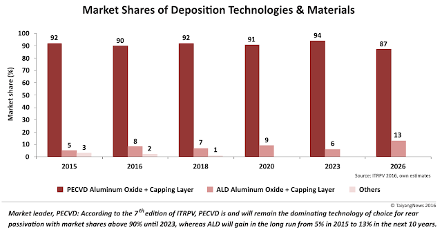
Here si a very good and detailed report by TaiyangNews on PERC solar cell technolygy that is free fo charge to doenload. Thnak you Roger Görtzen at SoLayTec for letting me know about this one. It shows a slow and steady growth for ALD Al2O3 back side passivisation the next 10 years. One of the major concerns for Al2O3 introduction u either PECVD or ALD is the cost of TMA. For ALD the industry seem to worry about that it is a new technoloogy and that you anyway need too cap of the Al2O3 with a silicon based dielectric PECVD process step. 

PERC Solar Cell Technology 2016 – Background, Status and Outlook provides an overview on background, status and outlook of promising high-efficiency silicon-based PERC cell technology.

All solar cell manufacturers that are evaluating capacity expansion in the current investment cycle have to decide if they stick to traditional technology or opt for advanced solutions. The simplest and most attractive silicon cell technology upgrade is called PERC, which stands for Passivated Emitter Rear Cell.


Our new report PERC Solar Cell Technology 2016 – Background, Status and Outlook provides an overview on background, status and outlook of PERC cell technology.
PERC is an advanced silicon cell architecture that comes with a promise of higher efficiencies. At the same time, it requires only minimal changes to existing solar cell processing lines. The concept is not new, it was invented in 1983 by well known Australian scientist Martin Green.
Opting for PERC means to add a rear passivation scheme to standard BSF cell technology. As for the implementation, it involves depositing a rear surface passivation film, which is subsequently opened to give way for formation of a rear contact. In addition, the chemical wet-bench based edge-isolation step is tweaked for rear polishing. The key aspect of PERC technology is to deposit the rear passivation film.
Our study provides background on the different rear passivation materials – the early silicon oxynitride and today state-of-the-art material, aluminum oxide.
The deposition of aluminum oxide can be accomplished by 4 well known deposition technologies that have been tweaked to apply this dielectric. While sputtering tools are currently not being offered for commercial production, there is little demand for APCVD. The two technologies for aluminum deposition mainly considered by commercial cell producers are PECVD and ALD. The study shows the pros and cons for each of these deposition technologies.
The report also delves into product details; nearly every deposition tool supplier is offering a package line for PERC. Short product descriptions are given on p. 29.
While the the first part of the study deals with equipment and material of PERC cells, we have also looked at the efficiencies and the performance potential at commercial scale. As new record efficiencies are quickly changing for PERC, commercialization of the technology is in full swing.
We estimate that 4.9 GW of PERC capacity was installed in 2015, resulting in about 3 GW of PERC cell production. The report also provides an estimate for 2016 PERC production.
Like any other technology, PERC faces challenges. The major concern is the so-called Light Induced Degradation (LID) effect, which, however, is especially associated with multicrystalline PERC cells today, but some companies already have this issue under control. In comparison, we also take a brief look at other high-efficiency cell concepts.
However, our overall impression is: PERC seems to be absolutely ready for prime time.

The Report can be downloaded free of charge here.

Saturday, April 9, 2016

A very warm welcome to RASIRC for sponsoring the ALD News Blog!

A very warm welcome to RASIRC as a new sponsor of the BALD Engineering ALD news blog! RASIRC based in San Diego California specializes in products that generate and deliver gas to fabrication processes. Each unit is a dynamic gas plant in a box—converting common liquid chemistries into safe and reliable gas flow for most processes. First to generate ultra-high purity (UHP) steam from de-ionized water, RASIRC technology can now also deliver hydrogen peroxide gas in controlled, repeatable concentrations.

RASIRC products that are in use for ALD include:
 
 
Next on the CMC Confernce 5-6th of May in Hillsoboro, Dan Alvarez, Chief Technology Officer of RASIRC will present their new technology for Hydrazine delivery in a talk entitled: "Hydrazine as a Low Temperature Nitride Source: Materials Challenges for High Volume Manufacturing"
 
You will be reading more about RASIRC here in the near future!


"ALD for Industry 2017" in Dresden open for Sponsoring & Exhibition

Ladies and Gentlemen,
 
As you may have noticed, Dresden has developed to the German Hotbed for ALD and we want to make you aware of an ALD event in Dresden early 2017 that may be very interesting for you to attend. The event will have a strong Industrial focus for ALD and you will be able to reach out to the German ALD market and your potential and existing customers here. 

This Event is organized in collaboration between members of "ALD Lab Dresden" and EFDS and is now open for Sponsoring & Exhibition booking. We have already had a good response from the ALD Equipment industry so hurry since number of exhibition tables will be limited!


ALD for Industry, 17-18 January 2017, Swissôtel Dresden Am Schloss

"This event provides the opportunity to learn more about fundamentals of ALD technology, to get informed about recent progress in the field and to get in contact with industrial and academic partners. Increase your visibility and present your company in our accompanying exhibition."

http://www.efds.org/appointments-detail/events/ald-workshop-ald-for-industry.html

More information will be available soon! 

Contact for Sponsoring:

Grit Kotschenreuther
kotschenreuther@efds.org
Tel. +49 351 8718372 


Thursday, April 7, 2016

Samsung Starts Mass Producing Industry’s First 10-Nanometer Class DRAM

Samsung just announced that they start Mass Producing Industry’s First 10-Nanometer Class DRAM now. According to the press release (here) the key technology developments include:
  • improvements in proprietary cell design technology
  • QPT - quadruple patterning technology lithography 
  • Ultra-thin dielectric layer deposition.
The two later ones should mean a lot of ALD business for High-k, Electrodes and dielectric spacers.

Below is a DRAM Technology Roadmap published by TechInsights last summer and here you can see that Samsung is nailing it and next we should expect announcements from SK Hynix and The Micron Camp.


Here is an earlier post form IEDM 2015 in December when Samsung revieled some details - if thoose are used here is unknown so hopefully some reverse engineering study will surface next:

Samsung to present low cost manufacturing of 20 nm DRAM and beyond at IEDM2015

Some advancement in keeping low cost manufacturing of 20 nm DRAM will be presented by Samsung at IEDM 2015. Key elements are:

  • avoiding EUV lithography
  • honeycomb structure (see figure below)
  • air-spacer technology


According to Solid State Technology an air-gap spacer arrangement achieves a 34% reduction in bitline capacitance for faster operation.

20nm DRAM: A New Beginning of Another Revolution (Invited), J. Park, Y.S. Hwang, S.-W. Kim, S.Y. Han, J.S. Park, J. Kim, J. W Seo, B.S. Kim, S.H. Shin, C.H. Cho, S.W. Nam, H.S. Hong, K.P. Lee, G.Y. Jin, and E.S. Jung, Samsung Electronics Co.


For the first time, 20nm DRAM has been developed and fabricated successfully without EUV lithography using the honeycomb structure and the air-spacer technology. These low-cost and reliable schemes are promising key technologies for 20nm technology node and beyond.


Plasma ALD 2015 in Review is completed!

Plasma-ALD.com has completed their 2015 review and published all the interesting statistics.  - very interesting stuff showing strong growth of Plasma ALD (PEALD).

"There was a lot of interesting plasma atomic layer deposition activities during 2015. I have found 237 references utilizing PEALD in one form or another that were accepted for publication during the year. That is a 63% increase over the 147 references found in 2014."


Top 3 is unchanged: South Korea, USA and Germany. Taiwan and The Netherlands moving up with a lot of publications in 2015.

Please go here to dig into the numbers: http://www.plasma-ald.com/

Wednesday, April 6, 2016

Beneq to present the most transparent Display and Spatial sheet-to-sheet ALD at ALD2016

Beneq has announced that they are to present the most transparent Display and Spatial sheet-to-sheet ALD at ALD2016. In three presentations at the event they will present the following :
  • Development of the world's most transparent display - enabled by ALD
  • Large area sheet-to-sheet spatial ALD system for high-throughput coating applications
  • ALD based 3D NIR filter and refractive index control for Rugate filters
Read the full story at the Beneq Blog here: http://beneq.com/blog/201604/platinum-presentations.html


ASM F-120 ALD Reactor for sale

Here is a classic ALD reactor for sale and it seems to be a rather new one since it is called ASM F-120 SAT ALCVD(TM) and not Microchemistry. A once in a life time opportunity!

Thanks to Brent Sperling for sharing this one and you can check it out here! on the Craiglist.


Monday, April 4, 2016

New Critical Materials Conference's Powerful Agenda


 Buy Reports  | CMC Fabs   |  CMC Conference  |  Register Now
New Critical Materials Conference's Powerful Agenda
May 5-6, Hillsboro Oregon
The Critical Materials Conference provides a framework to catalyze the flow of "actionable" technical and supply chain information related to critical materials. 

New Additions to the Critical Materials Conference Include: 
  • David Thompson, Ph.D., Director of Process Chemistry of Applied Materials
    • Agony in New Material Introductions - Minimizing and Correlating Variabilities
  • Suresh Ramalingam, Sr. Director, Advanced Packaging Development of Xilinx
    • Packaging Materials - Future Challenges 
A highly differentiated program, with networking opportunities for all attendees. 
For full agenda details click here.

Themes of the Conference are centered around the needs of the Critical Materials Council and the global IC fabrication industry. While executive conferences typically focus on the "what" and "why" of materials technologies, this conference will discuss "how" new materials can be controllably, safely, and cost-effectively used in fabs. The Conference will also include market data to validate "when" materials will be needed. Attendees from fabs, OEMs, and materials suppliers alike will have the opportunity to interact with the presenters and colleagues, to gain insights into best-practices of the entire supply-chain.
 
For more information on the conference go to www.cmcfabs.org/seminars/ 
Great Sponsorship Opportunities available, 
please contact cmcinfo@techcet.com or call 1-480-382-8336

Sponsors and Committee

Novel Negative Capacitance FET using a 5nm hafnium zirconium dioxide ferroelectric layer

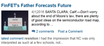
Here is an interesting story in EETimes on how "The Father of FinFET" Prof. Chenming Hu at Berkeley Device Modeling Center is promoting the Negative Capacitance Field efefct Transistor (NC-FET) based on a ferroelectric Hafnium Zirconium oxideintegrated into a standard HKMG Stack. The presenatation was hels as a Key Note "What Else Besides FinFET?" at the SNUG Silicon Valley 2016 · March 30 –31 · Santa Clara Convention Center organized by Synopsys.

http://www.eetimes.com/document.asp?doc_id=1329333&

 The gate stack under investiogation is a conventional thin HfO2 gate oxide with an added 5 nm ferrorelctric ZrO2:HfO2 layer before gate processing, which is a process that could be realized in anz sub 45 nm Fab today assuming you can etch a "thick" high-k gate oxide. The NC-FET development is supported by Intel and TSMC who joined joined, paying $140,000 each.


Chenming Calvin Hu is Distinguished Professor of Microelectronics at University of California, Berkeley. From 2001-2004, he was the Chief Technology Officer of TSMC, world’s largest IC foundry. (Wikipedia.org)

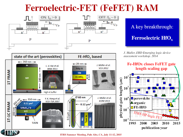
You have followed this Blog may have come across previos stories on the discovery and research on ferroelectric Hf-based metal oxides conducted in Dresden, German by NaMLab, Fraunhofer and Globalfoundries. Below is a small collection of those posts. One of the first materials systems besides Si:HfO2, Al:HfO2 and Y:HfO2 was the ZrO2:HfO2 system investigated by Johannes Müller (Fraunhofer IPMS). If this constallation also hare covering NC-FET, besides the work on FE-FETs and FRAM is not known. In any case, it will be continiously interesting to follow the forgress of ferroelectric ALD HfO2 based materials for novel devices!

Dresden Memory Startup To Debut At Semicon Europa

 FMC has been formed by NaMLab to commercialize the work and has taken over a publicly-funded program that will provide €500,000 (about $565,000) to cover development over the period April 2015 to September 2016. Meanwhile the small group of engineers that have formed the company are looking for early-stage investment and potential partners, Mueller said.

Ferroelectric HfO2 by ALD Key Breakthrough in ITRS “Beyond CMOS” Update 2015


Ferroelectric HfO2 Based Materials and Devices: Current Status and Future Prospects


Qimonda’s late legacy: 28nm FeRAM using ALD Ferroelectric HfO2

“This research goes back to 2007 at DRAM maker Qimonda, when a PhD candidate Tim Böscke was doing research to improve HfO2 as a high-k dielectric for capacitors in dynamic random access memories, using dopants to stabilize the material”, explained Mikolajiick. “At certain dopant concentrations and under specific treatments, Böscke noticed that strange peaks occurred in the CV characteristic of the material, and that it behaved as a ferroelectric. This was totally unexpected!"

Sunday, April 3, 2016

Atomic Layer Deposition at The CMC Conference, 5-6 May, Hillsboro, OR

For those of you that have a chance to attend the CMC Conference coming up in Hilsboro, 5-6th of May here is an updated List of Speakers. We are very happy to announce three key persons in from the ALD industry giving invited talks at this two day event  : 
  • Jean-Marc Girard from Air Liquide
  • S.I. Lee from Veeco
  • David Thompson from Applied Materials

In addtion, a number of invited talks related to ALD by Industry Leaders & Experts:
  • Rob Nine, Strategic Marketing - Pall Microelectronics 
  • Jeff. Hemphill, Sr. Materials Engineer - Intel Corp.
  • John Smythe, Ph.D., Advanced Technology Lead DMTS - MICRON Technologies
  • Max Kelman, Ph.D., Sr. Technology Manager – Aixtron 
  • Dan Alvarez, Ph.D., Chief Technical Officer - RASIRC
Check the schedule below for more details or go directly to the CMC Conference page here: http://cmcfabs.org/seminars/

Day 1, Session II:

Immediate Challenges of Materials & Manufacturing


Day 2, Session III, 1/2 Day:

Emerging Materials Challenges

UPDATE: ALD 2016 Dublin Speakers and Conference Programme


The conference programme for ALD 2016 has been updated with full information on Tutorials and Invited speakers!

Conference Timings:

Sunday 24 July:
Tutorial runs 13:00-17:00 in Convention Centre.  Welcome reception that evening in Guinness Storehouse.
Monday 25 July – Wednesday 27 July:
ALD2016 Conference will open at 8:15 in Convention Centre and closes at 17:45 on Wednesday 27 July followed by a gala dinner on Wednesday evening.


Conference Programme:

Tutorial on Atomic-Layer-Processing, Sunday 24th July:

Click on the speaker name to view their profile:
Speaker Organisation Presentation Title
Sumit Agarwal Colorado School of Mines USA Plasma Physics and Diagnostics
Keren Kanarik Lam Research, USA Overview of Atomic Layer Etching
Fred Roozeboom TU Eindhoven, The Netherlands Processing for 3D-IC Technologies
Sean Barry Carleton University, Canada ALD Precursor Design & Synthesis
Massimo Tallarida Alba, Spain, Characterization of ALD processes and Materials using Synchrotron Light
Annelies Delabie IMEC, Belgium Atomic layer processing of 2D materials for beyond CMOS applications
Stephan Wege Plasway GmbH, Germany Plasma Processing Reactor Design

Invited speakers:

Speaker  Organisation  Presentation title
Raymond Adomaitis University of Maryland Reaction Network Analysis for ALD Processes
Robert Clark TEL America
Byung Joon Choi Seoul National University of Science and Technology Multi-layered selector and switch devices enabled by atomic layer deposition for crosspoint memory
Mike Cooke Oxford Instruments
Jolien Dendooven University of Ghent Synchrotron-based characterization of Pt ALD
Michael Gros-Jean STMicroelectronics
Joseph Hupp Northwestern University
Ying-Bing Jiang University of New Mexico / Angstrom Thin Film Technologies LLC, USA
John Langan Air Products
Anatollii Malygin St Petersburg State Technological Institute
Yongfeng Mei Fudan University
Lars Samuelson Lund University Nanowire-based Technologies for Electronics, LEDs and Solar-cells
Further speakers, profiles and the conference programme will be published soon.  Please check back for information.

SoLayTec receives new ALD tool orders from PV solar cell manufacturers

SoLayTec today announced the continuing positive trend of incoming orders. Four new solar customers around the globe have ordered the Atomic Layer Deposition (ALD) equipment from SoLayTec. One of these customer is from Taiwan, and a mayor a step to open further opportunities for SoLayTec in this market. These shipments are scheduled to start within this quarter.

Depending on the capacity levels that are needed SoLayTec offers three types of InPassion ALD. Main difference is the number of deposition units modules added in such a system. The basic three products offered are 4, 6 or 8 deposition units, that respectively result into 2,500* wph, 3,600* wph or 4,800* wph. (www.solaytec.com)
Depending on the capacity levels that are needed SoLayTec offers two types of InPassion ALD. Main difference is the number of deposition units modules added in such a system. The basic two products offered are 4, 6 or 8 deposition units, that respectively result into 2,500* wph, 3,600* wph or 4,800* wph. - See more at: http://www.solaytec.com/products/inpassion-ald#sthash.y20MGE3A.dpuf
“After several years of having InPassion ALD systems in mass production at multiple customers in China and Japan, SoLayTec is delighted to announce that in the last couple of weeks 3 orders were received”, according Roger Görtzen, co-founder of SoLayTec and manager marketing and sales.


Field Replaceable Unit (optional FRU) - If one of the deposition units is not working properly and can’t be fixed by the customer or SoLayTec service team, this module or FRU will be replaced by another FRU. In this way the tool will be running as fast as possible at 100% capacity again. In parallel this FRU will be send to a SoLayTec service station to be refurbished.
  (www.solaytec.com)
“These machines will be used for production of high efficient solar cell concepts, like p-type PERC, n-type IBC and bi-facial cells. In the past SoLayTec announced that spatial ALD results in a higher efficiency of about 0,2% for multi and mono PERC cells compared to PECVD AlOx. At one leading PV solar cell manufacturer we have measured for ALD Al2O3 a surface recombination velocity between 1- 5cm/sec compared to ≥ 30cm/sec on similar material for PECVD AlOx . This data confirms that the passivation quality of ALD Al2O3 is factor ≥ 6 higher compared to PECVD AlOx. Recently, the c-Si wafer quality has been improved, and this results into better bulk material of the c-Si material. Consequently our customers request an excellent surface passivation which can be provided by ALD Al2O3 for their future cell concepts.” according Roger Görtzen. 
“So far, our customers were located in China, Japan and Europe so we are very happy with our newest market entrance in Taiwan. Now we have finally achieved this important milestone and of course SoLayTec will focus on further expansion of its footprint in this country.” said Roger Görtzen.

SoLayTec

SoLayTec is a spin-off company of the Dutch research organisation TNO and established in 2010. SoLayTec is part of the Amtech Group (Nasdaq ASYS). The company develops, delivers and services machines for atomic layer deposition (ALD) on solar cells worldwide. The SoLayTec ALD machines are designed for mass production in the solar market. In the field of solar cell ALD equipment, SoLayTec has a leading position.

For more information, please visit www.solaytec.com.