| ||||||||||
| ||||||||||
Header


%20(1).png)
Monday, July 20, 2015
JVSTA Special Issue on Atomic Layer Deposition Deadline Aug 30


The Ferroelectric Memory Company - FCM from Dresden
The FeFET is a
long-term contender for an ultra-fast, low-power and non-volatile memory
technology. In these devices the information is stored as a
polarization state of the gate dielectric and can be read
non-destructively as a shift of the threshold voltage. The advantage of a
FeFET memory compared to the Flash memory is its faster access times,
much lower power consumption at high data rates, and the easy
integration of the device with common high-k metal gate transistors in
complementary metal-oxide-semiconductor (CMOS) technology.
The basics of the idea of a were already laid in the early 2000s in the research department of the memory manufacturer Qimonda. The discovery of ferroelectricity in doped hafnium led there to the registration of several basic patents, which went to NaMLab gGmbH after the Qimonda insolvency.
In 2013 the proof of principle of a hafnium based ferroelectric field effect transistor (FeFET) memory cell on 28nm technology platform was manufactured at Globalfoundries Fab1 and Fraunhofer CNT in Dresden. There is a hope that the successful commercialization of such an embedded NVM memory technology could have disruptive character.

During the last years the electrical properties of ferroelectric
transistors were studied in detail. In the framework of a project
together with GLOBALFOUNDRIES and Fraunhofer CNT, which was funded by
the Free State of Saxony, silicon doped HfO2 layers were integrated into
high-k metal gate transistors in 28 nm CMOS technology. Depending on
the polarization state of the ferroelectric gate insulator a memory
window in the range of ~1.2 V threshold voltage shift can be reached.
Extrapolation of the measured memory window over time indicates a
retention time of 10 years with a remaining memory window of 0.4 V.
Functional devices with gate length down to ~30 nm were demonstrated.

Today Stefan Müller, Marko Noack and Jörg Andreasas a the team has started The Ferroelectric Memory Company - FCM and currently they are anchored to NaMLab gGmbH and benefits from a The EXIST Research Transfer-financing and support and mentorship by one of the leading semiconductor memory experts Prof. Thomas Mikolajick (Scientific director of NaMLab).

TEM of FeFET processed in 28 nm high-k metal gate CMOS Technology (left) and 2D TCAD-model for device simulation (right). (Picture from NaMLab)
Source (German) : https://www.futuresax.de/home/fuer-gruender/ideenwettbewerb/nominierte/team-energieeffiziente-speicher-60773.html
Source (English) : http://www.namlab.com/research/reconfigurable-devices/hafnium-oxide-based-ferroelectric-memory
SolarWorld AG new world record for PERC-technology solar cells
SolarWorld AG has set a new world record for efficiency of industrially produced solar cells made using so-called PERC-technology (passivated emitter and rear cell). The CalLab of the Fraunhofer Institute for Solar Energy Systems has confirmed that the global manufacturer of premium-quality products surpassed its own record by reaching a new height of 21.7 percent in its solar cell efficiency.
The cells, based on crystalline p-type silicon wafers, were manufactured using industrial production processes, meaning that they can be quickly placed into mass production. SolarWorld will offer modules with 300-watt and more featuring this technology beginning this fall.
“SolarWorld has been the first company to rely on PERC in its cell production. With this new record, we expand our technological lead even further. We can offer customers more electricity production on the same area and at the highest quality and durability,” says Dr.-Ing. E. h. Frank Asbeck, CEO of SolarWorld AG. “And our researchers and developers already have an eye on the next efficiency improvements.”
The passivation layer in PERC solar cells, which
reflects light that would otherwise be lost is, usually deposited by PECVD or ALD. I am waiting for a confirmation which process is used in the case of this world record.
Besi and Imec Present High-Accuracy Narrow-Pitch Bonding of 3D ICs using Thermocompression
As published by Imec at SEMICON WEST 2015 (San Francisco), world-leading nano-electronics research center imec and Besi, a global equipment supplier for the semiconductor and electronics industries announced that they have jointly developed an automated thermocompression solution for narrow-pitch die-to-wafer bonding, a method by which singulated dies are stacked onto bottom dies which are still part of a fully intact 300mm wafer. The solution features high accuracy and high throughput, paving the way to a manufacturable 2.5D, 3D, and 2.5D/3D hybrid technology.

Caption: 300 mm wafer with ~900 dies processed on Besi’s new 8800 TC bonder tool. Such an assembly can be finished within 1 hour.
3D IC technology, stacking multiple dies into a single device, aims to increase the functionality and performance of next-generation integrated circuits while reducing footprint and power consumption. It is a key technology to enable the next generation of portable electronics, such as smartphones and tablets, which require smaller ICs that consume less power.
One of the challenges to making 3D IC manufacturing an industrial reality is the development of a high-throughput automated process flow for narrow-pitch, high-accuracy die-to-die and die-to-wafer bonding. Thermocompression bonding (TCB) is a widespread process used by the industry for highly accurate die-to-package bonding. The method released the stress in the laminate layer and avoided stress to build up between the two stacked layers. Yet, more traditional approaches to thermocompression bonding come with long cycle times (>1 minute per die), meaning significant improvements in throughput are required to enable this stacking approach on a 300mm wafer.
Imec and Besi have developed an automated TCB process on 300 mm wafers for Besi’s new 8800 TC bonder tool. Imec and Besi demonstrated die-to-wafer bonding at high accuracy, sufficient for 50 µm pitch solder micro bump arrays and a throughput of >1000 UPH with a dual bond head configuration
“Collaborating with imec, leveraging their expertise on fine pitch bonding materials and processes, has enabled us to develop our 8800 TC bonder tool according to the needs of the semiconductor industry,” said Hugo Pristauz at Besi. “This collaboration has helped us to offer our customers a viable and effective solution for 2.5D/3D IC manufacturing, especially for the new C2W applications.”
Nanowires from TU/e give ‘solar fuel cell’ efficiency a tenfold boost
As published by TU Eindhoven - A solar cell that produces fuel rather than electricity. Researchers at
Eindhoven University of Technology (TU/e) and FOM Foundation today
present a very promising prototype of this in the journal Nature
Communications. The material gallium phosphide enables their solar cell
to produce the clean fuel hydrogen gas from liquid water. Processing the
gallium phosphide in the form of very small nanowires is novel and
helps to boost the yield by a factor of ten. And does so using ten
thousand times less precious material.

Array of nanowires gallium phosphide made with an electron microscope. Photo: Eindhoven University of Technology.
The electricity produced by a solar cell can be used to set off chemical reactions. If this generates a fuel, then one speaks of solar fuels – a hugely promising replacement for polluting fuels. One of the possibilities is to split liquid water using the electricity that is generated (electrolysis). Among oxygen, this produces hydrogen gas that can be used as a clean fuel in the chemical industry or combusted in fuel cells – in cars for example – to drive engines.
The electricity produced by a solar cell can be used to set off chemical reactions. If this generates a fuel, then one speaks of solar fuels – a hugely promising replacement for polluting fuels. One of the possibilities is to split liquid water using the electricity that is generated (electrolysis). Among oxygen, this produces hydrogen gas that can be used as a clean fuel in the chemical industry or combusted in fuel cells – in cars for example – to drive engines.
Solar fuel cell
To connect an existing silicon solar cell to a battery that splits the water may well be an efficient solution now but it is a very expensive one. Many researchers are therefore targeting their search at a semiconductor material that is able to both convert sunlight into an electrical charge and split the water, all in one; a kind of ‘solar fuel cell’. Researchers at TU/e and FOM see their dream candidate in gallium phosphide (GaP), a compound of gallium and phosphide that also serves as the basis for specific colored leds.
A tenfold boost
GaP has good electrical properties but the drawback that it cannot easily absorb light when it is a large flat surface as used in GaP solar cells. The researchers have overcome this problem by making a grid of very small GaP nanowires, measuring five hundred nanometers (a millionth of a millimeter) long and ninety nanometers thick. This immediately boosted the yield of hydrogen by a factor of ten to 2.9 percent. A record for GaP cells, even though this is still some way off the fifteen percent achieved by silicon cells coupled to a battery.
Ten thousand times less material
According to research leader and TU/e professor Erik Bakkers, it’s not simply about the yield – where there is still a lot of scope for improvement he points out: “For the nanowires we needed ten thousand less precious GaP material than in cells with a flat surface. That makes these kinds of cells potentially a great deal cheaper,” Bakkers says. “In addition, GaP is also able to extract oxygen from the water – so you then actually have a fuel cell in which you can temporarily store your solar energy. In short, for a solar fuels future we cannot ignore gallium phosphide any longer.”Reference
Anthony Standing et al., Efficient water reduction with gallium phosphide nanowires, Nature Communications (17 July 2015)
DOI: 10.1038/ncomms8824
Thanks to TG Techno to for posting this one! (http://tgtechno.com/nanotechnologyzone/)
Sunday, July 19, 2015
Self-Correcting Process For High Quality Patterning By Atomic Layer Deposition
An interesting publication using ALD for advanced pattering method which is a quite hot topic these days when lithography tools are swelling in all directions and just getting slower - The research is from the Bent Research Group at Stanford University!

Self-Correcting Process For High Quality Patterning By Atomic Layer Deposition.
Minaye Hashemi FS, Prasittichai C, Bent SF.

Schematic demonstrating self-aligned patterning through a combination of
selective deposition (using ODPA SAM blocking layer on Cu oxide) and
selective removal (using acid) of dielectric material. (Graphical abstract ACS Nano, Article ASAP,DOI: 10.1021/acsnano.5b03125)
Nanoscale patterning of materials is widely used in a variety of device applications. Area selective atomic layer deposition (ALD) has shown promise for deposition of patterned structures with sub-nanometer thickness control. However, the current process is limited in its ability to achieve good selectivity for thicker films formed at higher number of ALD cycles. In this report, we demonstrate a strategy for achieving selective film deposition via a self-correcting process on patterned Cu/SiO2 substrates. We employ the intrinsically selective adsorption of octadecylphosphonic acid self-assembled monolayers on Cu over SiO2 surfaces to selectively create a resist layer only on Cu. ALD is then performed on the patterns to deposit a dielectric film. A mild etchant is subsequently used to selectively remove any residual dielectric film deposited on the Cu surface while leaving the dielectric film on SiO2 unaffected. The selectivity achieved after this treatment, measured by compositional analysis, is found to be ten times greater than for conventional area selective ALD.
Saturday, July 18, 2015
Growth forecast for Wafer Fab Equipment and ALD according to Gartner
Good news of ALD - Gartner has forecasted a growth for the Advanced nodes to come!
Gartner says that the Worldwide semiconductor revenue is forecast to reach $348 billion in 2015, a 2.2 percent increase from 2014, but down from the previous quarter's forecast of 4.0 percent growth, according to Gartner, Inc.

Growth forecast for Wafer Fab Equipment according to Gartner (Graph from ASMi Investor Technology Seminar at SEMICON West)
"The outlook for the major applications that drive the semiconductor market, including PCs, smartphones, and tablets, have all been revised downward. This, combined with the impact of the strong dollar on demand in key markets, has resulted in a lower semiconductor forecast for 2015," said Jon Erensen, research director at Gartner. "The typical second-quarter bounce did not materialize this year, and as a result, the semiconductor industry is more back-end loaded and dependent on a strong third-quarter rebound, driven by Windows 10 and the ramp-up to the holiday season.”
From an application point of view, smartphones and solid-state drives (SSDs) will continue to drive semiconductor market growth, while the traditional PC segment will experience the greatest decline, with production units down 8.7 percent in 2015, slightly weaker than the previous quarter's forecast. "Inventory in the PC market remains high despite vendors looking to clear the supply chain in anticipation of Windows 10 and Intel's Skylake products. Any issues with the launches of Windows 10 or Skylake in the third quarter of 2015, which are expected to reinvigorate PC sales, could lead to further decline," said Mr. Erensen.
In the smartphone market, Apple's iPhone is the bright spot for the market with strong unit growth and increasing average selling prices (ASPs), driven by the strong performance of the iPhone 6 and iPhone 6 Plus. However, lackluster performance in high-end Android smartphones and general softness in the smartphone market in China will continue to impact growth.
Although the wearables market, including smartwatches, head-mounted displays (HMDs), smart glasses and Bluetooth headsets, is a growing industry, revenue for wearables semiconductors — processing, sensing and communications chips — will represent only 1 percent of total semiconductor revenue by 2019. Smartwatches are the top semiconductor growth in the near term.
From a device point of view, DRAM continues to be one of the primary growth drivers of the overall industry. DRAM revenue is expected to increase 3.8 percent in 2015, following a 32 percent increase in 2014. However, Gartner expects an oversupply (or "underdemand") to develop in 2016 as limited new capacity comes online and technology migration continues. DRAM industry revenue is expected to decline 17.4 percent in 2016 and 7 percent in 2017.
"The typical second-quarter bounce did not materialize this year, and as a result, the semiconductor industry is more back-end loaded and dependent on a strong third-quarter rebound, driven by Windows 10 and the ramp-up to the holiday season," said Mr. Erensen.
Wednesday, July 15, 2015
16th International Conference on Atomic Layer Deposition, 24th-27th July 2016, Dublin
The 16th International Conference on Atomic Layer Deposition (ALD 2016) will be a three-day meeting dedicated to the science and technology of atomic layer controlled deposition of thin films. In every year since 2001 at Monterey, the conference has been held alternately in United States, Europe and Asia, allowing fruitful exchange of ideas, know-how and practices between scientists. The conference will take place on 24-27 July 2016 at the Convention Centre Dublin, Ireland.

Atomic Layer Deposition (ALD) is used to fabricate ultrathin and conformal thin film structures for many semiconductor and thin film device applications. A unique attribute of ALD is that it uses sequential self-limiting surface chemistry to achieve control of film growth in the monolayer or sub-monolayer thickness regime. ALD is receiving attention for its applications in leading-edge electronic technologies, advanced microsystems, displays, energy capture and storage, solid state lighting, biotechnologies and medical technologies. Indeed ALD is particularly advantageous for any advanced technology that requires control of film structure in the nanometer or sub-nanometer scale.
As in past conferences, the meeting will be preceded by one day of tutorials. An industry trade show will be held in conjunction with the conference, to act as common ground for academia and industry to meet and discuss the future applications of ALD. Extra opportunities for collaboration will be provided through working groups of the COST Action ‘Hooking together European research in atomic layer deposition (HERALD)’.
The presentations will be recorded and electronic copies of the presentations (including oral component, questions/answers and posters) will be made available in the form of copy-secured DVDs.
This conference offers an excellent opportunity to learn about the most recent R&D activities in ALD science and technology from researchers around the world. We look forward to your participation.
ALD 2016 Co-Chairs:
 |  |
| Simon Elliott Tyndall National Institute, Ireland | Jonas Sundqvist Division of Solid State Physics, Lund University, Sweden |
Key Dates
Registration opens: Friday, 1st January 2016.Early bird registration closes: Thursday, 31 March 2016.
Abstract submission opens: Monday, 30th November 2015.
Abstract submission closes: Sunday, 14th February 2015.
Author notification: Sunday, 21st May 2016.
Conference opens: Sunday, 24th July 2016.
Conference concludes: Wednesday, 27th July 2016.

Photos from recent Workshop on Fundamentals of ALD - Eindhoven - are online
Here are a lot of nic oictures from the this recent event:
http://nanomanufacturing.nl/photos.php

"The aim of the workshop is to spark a discussion about current topics in
the field of atomic layer deposition (ALD) by addressing fundamental
aspects of the method. It is expected that this discussion will lead to
new and refined insights beneficial to further advance the field of ALD.
The aim is to serve both scientists who work at the forefront of ALD
research as well as newcomers and technologists who want to get a better
understanding of ALD."
ALD of Transparent Semiconducting Oxide CuCrO2 for Invisible electronics
So you learn something new every day and as before and so many times also this time from Aalto University, Helsinki Finland! ALD of Transparent Semiconducting Oxide CuCrO2 for Invisible electronics! Some basic facts from this excellent ALD paper :
- Copper chromium oxide CuCrO2 is a member of the delafossite family CuAO2 (A = Al, Cr, Fe, Co, Ga, Y, In, La, Nd, and Eu.
- With predominantly antiferromagnetic interactions, members of this family possess a geometrically frustrated (!) triangular lattice
- The discovery of simultaneous p-type electrical conductivity and optical transparency in CuAlO2 thin films opened the new venue of research among delafossites for ‘invisible electronics’
- CuCrO2 is reported to have the highest electrical conductivity (220 S/cm) among the delafossite materials.
- The need for p-type TCOs stems from the realization of transparent electronics; that by far depends on the p-type semiconductor materials for use in transparent p–n and p–i–n diodes.
- Materials with a wide bandgap (>3 eV), high electrical conductivity, high mobility, low fabrication cost along with controllable transparency would be a boom for transparent electronics.
So there is an industrial need for high performing TCO material (we knew that, see Mr Lytle below) with low production cost (always the case) with additional material properties and a upcoming disruptive technology - Invisible Electronics. Doesn´t look like CVD and PVD can make all this - As always ALD must be up for the challenge!

William O. Lytle the inventor of Electric glass so called Nesa coated glass (Science 1946, Sep. 16) showing of his product which in a way is one of teh first invisible electronic devices. Note that he is using rather thick rubber gloves to not disturb the device... [http://publica.fraunhofer.de/documents/N-313429.html]
Atomic Layer Deposition of Transparent Semiconducting Oxide CuCrO2 Thin Films
Tripurari S. Tripathi, Janne-Petteri Niemelä and Maarit KarppinenJ. Mater. Chem. C, 2015, Accepted Manuscript
DOI: 10.1039/C5TC01384D
Atomic layer deposition (ALD) is a vital gas-phase technique for atomic-level thickness-controlled deposition of high-quality thin films on various substrate morphologies owing to its self-limiting gas-surface reaction mechanism. Here we report the ALD fabrication of thin films of the semiconducting CuCrO2 oxide that is a highly prospective candidate for transparent electronics applications. In our process, copper 2,2,6,6-tetramethyl-3,5-heptanedionate (Cu(thd)2) and chromium acetyl acetonate (Cr(acac)3) are used as the metal precursors and ozone as the oxygen source. Smooth and homogeneous thin films with an accurately controlled metal composition can be deposited in the temperature range of 240–270 oC; a post-deposition anneal at 700-950oC in an Ar atmosphere then results in well crystalline films with the delafossite structure. The direct bandgap is determined from UV-vis spectrophotometric measurements to be 3.09 eV. The observed transmittance is greater than 75% in the visible range.
Imec introduces self-assembled monomolecular organic films to seal ultra-porous low- k materials
Nano-electronics research center imec announced today at SEMICON West that it has demonstrated concept and feasibility for pore-sealing
low-k dielectrics in advanced interconnects. The method, based on the
self-assembly of an organic monolayer, paves the way to scaling
interconnects beyond N5.

RC plot and HAADF-STEM images illustrating the effectiveness of SAM sealing in preventing metal indiffusion into the ultra-porous low-k film integrated in a 45nm half pitch dual damascene test vehicle. This translates in a 30% decrease in the measured capacitance. (www.imec.be)
The need for ultra-porous low-k materials as interconnect dielectrics to meet the requirements dictated by the ITRS (International Technology Roadmap for Semiconductors) poses several challenges for successful IC integration. One of the most critical issues is the indiffusion of moisture, ALD/CVD metal barrier precursors and Cu atoms into the porous low-k materials during processing (low-k pore diameter larger than 3nm, up to 40% porosity). This leads to a dramatic increase of the material dielectric constant and leakage current, and to the reduction of the voltage for dielectric breakdown.

Imec has developed a method to seal the pores of the low-k material with a monomolecular organic film. The method not only prevents diffusion of moisture and metal precursors into the low-k material, it also might provide an effective barrier to confine copper within the copper wires and prevent copper diffusion into the low-k material.
Self-assembled monolayers (SAMs) derived from silane precursors, are deposited from vapor phase on 300mm wafers into low-k during chemical vapor or atomic layer deposition and subsequent Cu metallization. The dielectric constant (k) of the resulting sealing layer is 3.5 and a thickness lower than 1.5nm was achieved. This is key to limit the RC delay increase enabling beyond 5nm technology nodes. As a result, a ca. 30% capacitance reduction was observed after SAM pore-sealing was applied. Moreover, a clear positive impact on the low-k breakdown voltage is observed upon sealing.
Tuesday, July 14, 2015
Advanced Metallization Scheme for 3 x 50 um TSV Middle Process – IMEC
Here are some highly interesting insights to the latest Imec process technology for TSVs using a number of advanced Lam Research processing platforms including ALD - As reported by Solid State Technology, By Dr. Phil Garrou, Contributing Editor (I spiced it up with some nice Lam Research chamber pictures):
Scaling down the TSV diameter from 5μm to 3μm is very attractive for the 3D IC implementation in more advanced CMOS nodes. For instance, stress caused by the mismatch between the coefficient of thermal extension (CTE) of Si and Cu may generate strain in the Si around the TSV, degrading the device performance of transistors located close to a TSV. To reduce the impact on transistors, a so called keep-out-zone (KOZ), is generally defined around the 3D TSVs. This keepout-zone is however significantly smaller when scaling down the TSV diameter from 5μm to 3μm. When increasing the aspect ratio of the TSV from 10:1 to 17:1 (for 3μm diameter and 50μm depth), the conventional PVD barrier and seed options reach their conformality limits. Very thick barrier/seed layers need to be deposited in order to assure a continuous film at the bottom of the TSV. This not only fundamentally limits the extendibility of this integration scheme, but also increases the PVD deposition cost itself and the required CMP time, among other technical challenges. For these reasons, a new advanced and scalable TSV metallization scheme was developed.

Atomic layer deposition (ALD) has emerged as a key enabling technology for conformal film applications such as TSV oxide liner. Typical step coverage or conformality of other CVD oxide films is only 60-75% for high aspect ratio TSVs . In contrast, the VECTOR ALD oxide film shows 100% con formality.

Lam Research VECTOR ALD process chambers (www.lamresearch.com)
ALD WN serves as a barrier layer and is deposited on the Altus Max tool. It is highly conformal with >90% step coverage regardless of geometry. ALD WN is deposited at 375°C and has excellent adhesion to ALD oxide and subsequent ELD NiB. The conformality of the ALD process results in a pinhole-free WN layer, as opposed to barriers deposited by PVD, which potentially struggle with pinholes at the bottom of high aspect ratio TSV.

Lam Research Altus Max Chambers (www.lamresearch.com)
NiB electroless deposition on WN barrier was carried out on a Lam ELD2300 tool using a plating chemistry developed at Lam. The entire deposition process was made of several sequential steps such as a brief pre-clean, activation, deposition, rinse and dry. The concentration of reducing agent and nickel ions as well as the pH and temperature are controlled to maintain optimum deposition condition for seed formation during the NiB deposition. After deposition of ELD NiB, TSV copper electrofill is processed on a Lam SABRE 3D electroplating system using an industry standard acid copper sulfate electrolyte with a Lam

Lam Research SABRE 3D Electroplating system (www.lamresearch.com)
exclusive organic additive package. The conductivity and corrosion resistance of the Lam ELD NiB film enable compatibility with the electrofill process on 300mm wafer scale. Bottom-up fill of the vias proceeds without the need for the additional copper seed film that has been used with other conformal metal liners (e.g. Co or Ru).
Because of the high conformality of liner, barrier and seed layers, this proposed Via-middle metallization scheme is believed to be scalable to even higher aspect ratio TSVs with 2μm diameter.
HAM-LET Introduces Ultra High Purity Hoses and Alloy C-22 Fittings at Semicon West 2015
HAM-LET, a leading global manufacturer and provider of instrumentation solutions and components for high purity application and industrial fluid and gas delivery systems, will showcase various unique technologies at Semicon West 2015 in Moscone Center, San Francisco, USA, during July 14-16, booth no.1539.

HAM-LET is a leading solutions and products provider for the largest companies in the Semiconductor market, offering high purity products with outstanding durability and low maintenance. Working closely with its customers, HAM-LET is continuously upgrading its manufacturing processes and technologies, as well as vastly extending the use of exotic alloys, to comply with the required ultra-high purity (UHP) standards.
Nickel Alloys are known throughout the chemical process industry as premier corrosion resistant materials. HAM-LET utilizes alloy C-22 valves and fittings. This alloy is a most versatile nickelchromium-molybdenum-tungsten alloy available today with improved resistance to both uniform and localized corrosion, as well as to a variety of mixed industrial chemicals. Alloy C-22 exhibits superior weldability for improved resistance to corrosion, as well as offering an ultra-smooth surface finish, rated at 5RA.

HAM-LET Ultra High Purity (UHP) Flexible Hoses are made from stainless steel and other various materials. They are Electro-Polished for high purity and clean applications. Their whole manufacturing process takes place in clean rooms rated as class 10, as done for all HAM-LET high purity products. The UHP hoses can be connected to various end connections according to customer requirements; these include HAM-LET's High and Ultra High Purity Fittings (HTC), Ultra Clean Valves (UCV) as well as HAM-LET unique Let-Lok® fittings. Let-Lok® Fittings operate in extreme temperatures ranging from: -320°F (-196°C) to 932°F (500°C) and can be connected to Ultra High Purity hoses as well as to other devices.
HAM-LET provides solutions as well as a complete suite of products for the semiconductor and other high purity sectors; many products are available in stock and others can be customized per specific requirements.
Germany to fund the Semiconductor industry with 400 milion Euro
"Every second chip made in Europe comes from Saxony!"
Happy days in Dresden, Silicon Saxony and Germany today - Yesterday Globalfoundries announced that they are investing in Fab 1 in Dresden to ramp 22 nm FD-SOI and today Angela Merkel and Johanna Wanka comes for a visit to Dresden and promises 400 million Euro support package until 2020 for the semiconductor industry!
"Um Innovationen in der Halbleiterindustrie auch künftig voranzutreiben,
erarbeitet das Bundesforschungsministerium bis Ende des Jahres zusammen
mit weiteren Ressorts ein neues Rahmenprogramm. Das Programm soll mit
einem Volumen von 400 Millionen Euro bis 2020 ausgestattet werden. Das
hat Bundesforschungsministerin Wanka bei ihrem Besuch in Dresden
angekündigt. " - http://www.bmbf.de/de/28961.php
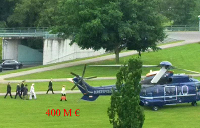

Chancellor Angela Merkel entering the helicopter in Berlin to fly 200 km south to Dresden. (Twitter, BMBF)

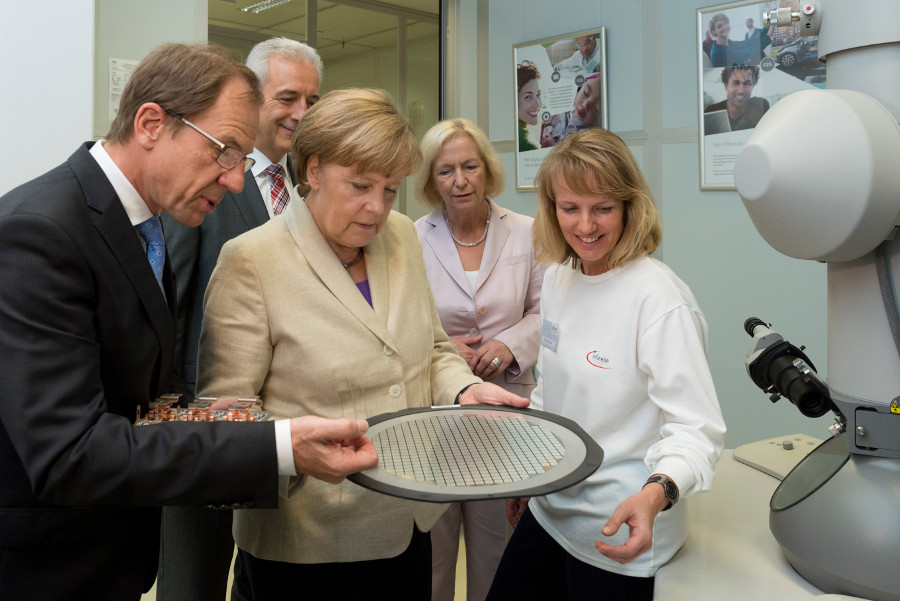
Rutger Wijburg (VP and General Manager Fab1, Dresden) explains factory physics for Sanjay Jha (CEO Globalfoundries) Chancellor Angela Merkel, Ministerpräsident Stanislaw
Tillich and Bundesforschungsministerin Johanna Wanka using a model Globalfoundries Fab 1 in
Dresden. (Photo: Heiko Weckbrodt)
More details for those of you reading German can be found in the excellent coverage by Heiko Weckbrodt :
Kanzlerin Merkel debattiert in Dresden Mikroelektronik-Strategie
MDR Sachsen Video in German:
Overview
http://www.mdr.de/sachsenspiegel/video284012.html
Silicon Saxony
http://www.mdr.de/sachsenspiegel/video284020.html
Globalfoundries
http://www.mdr.de/sachsenspiegel/video283788.html
MDR Sachsen Video in German:
Overview
http://www.mdr.de/sachsenspiegel/video284012.html
Silicon Saxony
http://www.mdr.de/sachsenspiegel/video284020.html
Globalfoundries
http://www.mdr.de/sachsenspiegel/video283788.html

Later Frau Bundeskanzlerin Dr Merkel also stopped by Fraunhofer to meet with The Fraunhofer President Prof. Dr. Reimund Neugebauer.
Angela Merkel also visited Infineon’s Dresden 300 and 200 mm fabs today and discussed the political framework for a competitive development and production in Germany with CEO Reinhard Ploss. - See more at: http://www.electronicsweekly.com/news/business/merkel-visits-infineon-dresden-fab-2015-07/#sthash.XHTLv12Y.dpuf

Yesterday, flanked by two clean room engineers posing with 300 mm device wafers the Globalfoundries Managers Gregg Bartlett, Sanjay Jha (CEO) und Rutger Wijburg (VP and General Manager Fab1, Dresden) announce that Globalfoundries will invest $250 million for 22nm FD-SOI production in Fab 1 Dresden, Germany. From the press conference in Dresden (photo by Heiko Weckbrodt, www.computer-oiger.de)
UPDATE: ASM International technology briefing SEMICON West 2015
ASM International N.V. announces that it
will be hosting an analyst and investor technology briefing on
Wednesday, July 15, 2015 at 8:00 - 9:30 a.m. (PDT) in San Francisco, US,
coinciding with SEMICON West 2015. The presentation will be held in
Room 301, Esplanade, Moscone Center.

ASMi is operating in a very close relationship with leading IDMs and Imec on CMOS scaling. In this
technology seminar Han Westendorp, Vice President Corporate Marketing,
will present "Advanced wafer processing with new materials". The
presentation will include highlights of ASM's
- Advanced thermal ALD
- Plasma enhanced ALD products and technologies
- CVD, PECVD and epitaxy technologies
The excellent presentation has now been released and can be downloaded here and some highlights you can find below:
http://www.asm.com/Downloads/2015_Semicon_West_investor_technology_seminar_presentation.pdf
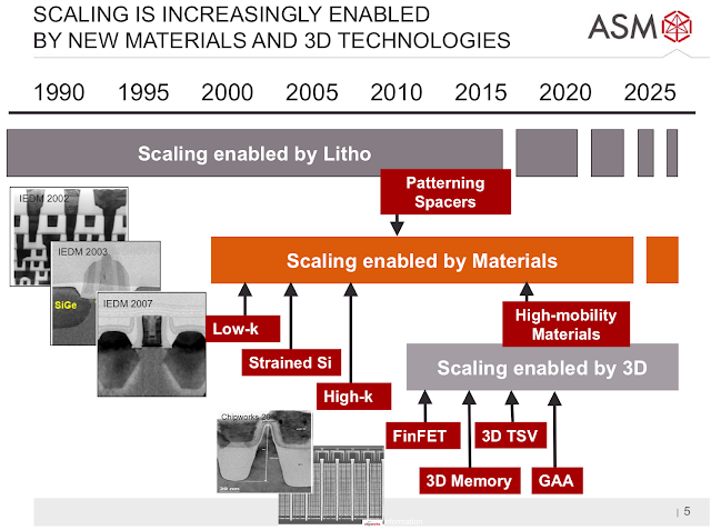


How scaling has been enabled by the introduction of new material and 3D integration.

Density scaling (continuing Moore’s law) driving towards higher mobility materials and alternate device architectures. Future systems will integrate much wider variety of materials and device structures


Here is a nice growing list of the materials and processes that has been introduced until now to drive scaling forward. Many of these process are perfumed by either Epitaxy, CVD/PECVD or ALD/PEALD.
Applied Materials announced a next-generation etch tool at SEMICON West
Applied Materials, Inc. announced a next-generation etch tool at SEMICON West, the Applied Centris(TM) Sym3(TM) Etch system,
featuring an entirely new chamber for atomic-level precision
manufacturing. To overcome within-chip feature variations, the Centris
Sym3 system leapfrogs current tools to provide chipmakers with the
control and precision needed to pattern and create densely packed 3D
structures in advanced memory and logic chips.

Applied Materials Centris
Sym3 - an entirely new chamber for atomic-level precision
manufacturing
"Drawing
on over 20 years of etch learning and our expertise in precision
materials removal, the Sym3 system represents a brand new design, built
from the ground up, that solves persistent and impending industry
challenges," said Dr. Raman Achutharaman, vice president and general
manager of Applied's Etch business unit. "Customer traction has been
remarkable, resulting in the fastest adoption rate we've seen for an
etch tool in the company's history, with record ramp to production at
leading-edge fabs."
The Centris Sym3 etch chamber
employs Applied's unique True Symmetry(TM) technology with multiple
tuning controls for optimizing global process uniformity to the atomic
level. Key to the design is a focus on controlling and removing etch
byproducts, which are increasingly hampering within-chip patterning
uniformity. The system mitigates byproduct re-deposition to overcome the
challenges of line edge roughness, pattern loading and defects -
issues that are becoming more limiting for each successive technology
node. Combined with an advanced RF technology that controls ion energy
and angular distributions, the Sym3 system delivers unsurpassed vertical
profiles for high aspect ratio 3D structures.
The
Centris Sym3 platform's six etch and two plasma clean process chambers
feature system intelligence software to ensure that every process in
every chamber matches precisely, enabling repeatability and high
productivity for high-volume manufacturing.
Imec and Panasonic Demonstrate Breakthrough RRAM Cell
Imec and Panasonic Corp. announced today that they have fabricated a 40nm TaOx-based RRAM (resistive RAM) technology with precise filament positioning and high thermal stability. This breakthrough result paves the way to realizing 28nm embedded applications. The results were presented at this year’s VLSI technology symposium (Kyoto, June 15-19 2015).

Cross-sectional TEM of 40-nm Ir(TE)/Ta2O5/TaOx/TaN (BE) RRAM
One of today’s most promising concepts for scaled memory is RRAM which is based on the electronic (current-or voltage-induced) switching of a resistor element material between two metals. Imec and Panasonic developed a method that overcomes filament instability in RRAM, one of the critical parameters that impacts the memory state during read operation in resistive memory.
The method was realized using a combination of process technologies such as low-damage etching, cell side oxidation, and an innovative encapsulated cell structure with an Ir/Ta2O5/TaOx/TaN stacked film structure featuring a filament at the cell center. With these methods, a 2-Mbit 40nm TaOx-based RRAM cell with precise filament positioning and high thermal stability was achieved. The memory array showed excellent reliability of 100k cycles and 10 years’ retention at 85°C. Additionally, the filament control and thermal stability technologies offer the potential to realize 28nm cell sizes.
Gosia Jurczak, director of imec’s research program on RRAM devices stated: “With these breakthrough results, we have proven the potential of this promising memory concept as embedded nonvolatile memory in 28nm technology node where conventional NOR Flash shows scaling limitations. This result is a confirmation of our leadership position in research and development on resistive memory.”
Monday, July 13, 2015
Lam Research Releases High-Productivity VECTOR(R) ALD Oxide Deposition System
Lam Research Corp a major global supplier of innovative wafer fabrication equipment and services to the semiconductor industry, today announced it has released its high-productivity VECTOR® ALD Oxide system on the Extreme platform. The new product uses atomic layer deposition (ALD) to create highly conformal dielectric films with an emphasis on advanced patterning, in particular spacer-based multiple patterning. One key challenge is managing thickness variability of the self-aligned spacers that define critical dimensions (CDs). By delivering superior CD control, VECTOR ALD Oxide has been winning volume-production decisions for multi-patterning applications. Now leveraging Lam's Extreme platform, the latest system meets productivity requirements for continued scaling, where additional steps increase process time, cost, and complexity. As a result, VECTOR ALD Oxide is gaining rapid adoption by a number of leading chipmakers for advanced multi-step patterning applications.

"Multiple patterning continues to be a key inflection for the industry, and spacer-based multi-patterning remains an enabling strategy for chipmakers for both current immersion and future EUV lithography schemes," said Sesha Varadarajan, group vice president, Deposition Product Group. "With this in mind, we are working closely with our customers to deliver cost-effective, extendible solutions required for further scaling, such as the high-productivity atomic-scale control from our VECTOR ALD Oxide product."
By repeating lithography/etch/deposition steps, multiple patterning techniques create smaller features and higher feature densities compared to the capability of current optical lithography using single patterning. To enable scaling for 14 nm and below, chipmakers are adopting self-aligned schemes, including self-aligned double patterning (SADP) and self-aligned quadruple patterning (SAQP), where deposition plays a critical role in forming the pattern-defining spacers. These deposition processes are challenging since they must form high-quality conformal and very uniform films. For example, a 200-300 angstrom-thick film can have only a few angstroms thickness variation across the wafer. For next-generation 10 nm processes, the manufacturing complexity will continue to increase as additional multi-patterning process steps are added, with each step contributing to overall CD variability.
Using Lam's advanced ALD capabilities, the latest VECTOR ALD Oxide system delivers the uniformity required for CD control of the ultra-thin films critical to SADP and SAQP schemes. The quad-station modules process four wafers simultaneously and share components to improve reliability and chamber matching, contributing to industry-leading wafer-to-wafer repeatability performance. The system's compact design delivers as much as 20% higher footprint productivity compared with other solutions. Process hardware has also been optimized to enable fast gas and RF switching, increasing throughput and reducing precursor usage for improved running costs. These innovative process module features combined with the high-productivity platform deliver the performance and cost-efficiency needed for manufacturing. Consequently, VECTOR ALD Oxide is winning development and production tool of record positions at leading manufacturers for advanced multi-patterning applications. This momentum is being successfully expanded to other applications, such as high-aspect ratio liners for through-silicon vias (TSVs) and image sensors.
Applied Materials to introduce a new system for Atomic Layer Deposition - Olympia™ ALD
Woah - this one we all have been waiting for - a paradigm shift in ALD processing by Applied Materials! I have not checked out all the details yet and yes it is a Spatial ALD machine and I am stunned with what I have seen so far : As announced today - Applied Materials to introduce a new system for Atomic Layer Deposition - Olympia™ ALD. Continued process scaling is driving new levels of device performance. ALD
is essential for a growing number of the device-critical process steps
in 3D NAND and logic FinFET fabrication. However, while the conformality
and uniform film thickness achieved with ALD is still vital for CD
control, additional demands are being made on ALD to deliver a growing
range of high-quality, robust films within restrictive thermal budgets
of next-generation nodes.


The Applied Olympia™ ALD system for
stand-alone deposition of dielectric and metal films solves the
significant challenge of obtaining high-quality ALD films at the low
deposition temperatures needed to fabricate planar and 3D devices at
next-generation nodes, delivering a new class of high-performance ALD.


Today’s
ALD involves not only laying down a film by depositing a succession of
layers each one atom thick. The process is also often accompanied by
materials engineering (treatments) required to impart specific
properties to these films. The Olympia system’s capabilities extend well
beyond conventional solutions, performing the dual functions of
deposition and materials engineering through flexible modular design.
This modularity offers unmatched sequencing capabilities that solve the
significant challenge of obtaining high-quality films at the low
deposition temperatures required to manufacture today’s leading-edge
memory and logic chips. The flexible design also enables the system to
accommodate the wide variety of precursors and process/treatment
combinations that will be needed to deliver the quality, diversity and
thermal range of ALD processes anticipated for future generations of
devices.
Video - In the Olympia chamber, wafers rotate through isolated zones of different chemistries. Here, each wafer is exposed to two chemistries in series; they react at the wafer surface to create a conformal monolayer of film. An additional monolayer is deposited with every exposure cycle. Treatment processes can be incorporated into the sequence for atomic-level materials engineering to meet specific customer needs.

The Olympia ALD system is differentiated by innovative chemistry management that ensures absolute separation of the individual precursors used in the deposition process. This unique feature is crucial for minimizing the creation of potentially damaging byproducts and particles that can form when chemistries mix freely. Consequently, the system generates exceptionally few defects, running for extended periods between chamber cleanings. Furthermore, the system offers a more than 50 percent productivity benefit over conventional, time-separated ALD by eliminating the pump/purge step after each chemistry.
According to Solid State Technology Applied Materials formed a Patterning Group about a year ago, led by Prabu Raja, group vice president. The group handles etch, CVD, selective material removal and ALD. “The growth there has been tremendous,” Dickerson said. Dickerson said they have moved $400 million of investment in the company into these opportunities and into new products.
According to Solid State Technology Applied Materials formed a Patterning Group about a year ago, led by Prabu Raja, group vice president. The group handles etch, CVD, selective material removal and ALD. “The growth there has been tremendous,” Dickerson said. Dickerson said they have moved $400 million of investment in the company into these opportunities and into new products.
GLOBALFOUNDRIES Launches Industry’s First 22nm FD-SOI Technology Platform in Dresden
GLOBALFOUNDRIES today launched a new semiconductor technology developed
specifically to meet the ultra-low-power requirements of the next
generation of connected devices. The “22FDX™” platform delivers
FinFET-like performance and energy-efficiency at a cost comparable to
28nm planar technologies, providing an optimal solution for the rapidly
evolving mainstream mobile, Internet-of-Things (IoT), RF connectivity
and networking markets.
Flanked by two clean room engineers posing with 300 mm device wafers the Globalfoundries Managers Gregg Bartlett, Sanjay Jha (CEO) und Rutger Wijburg today announced at a press event that Globalfoundries will invest $250 million for 22nm FD-SOI production in Fab 1 Dresden, Germany.

Flanked by two clean room engineers posing with 300 mm device wafers the Globalfoundries Managers Gregg Bartlett, Sanjay Jha (CEO) und Rutger
Wijburg (VP and General Manager Fab1, Dresden) announce that Globalfoundries will invest $250 million for 22nm FD-SOI production in Fab 1 Dresden, Germany. From the press conference in Dresden (photo by Heiko Weckbrodt, www.computer-oiger.de)
While some applications require the ultimate performance of three-dimensional FinFET transistors, most wireless devices need a better balance of performance, power consumption and cost. 22FDX provides the best path for cost-sensitive applications by leveraging the industry’s first 22nm two-dimensional, fully-depleted silicon-on-insulator (FD-SOI) technology. It offers industry’s lowest operating voltage at 0.4 volt, enabling ultra-low dynamic power consumption, less thermal impact, and smaller end-product form-factors. The 22FDX platform delivers a 20 percent smaller die size and 10 percent fewer masks than 28nm, as well as nearly 50 percent fewer immersion lithography layers than foundry FinFET.
“The 22FDX platform enables our customers to deliver differentiated products with the best balance of power, performance and cost,” said Sanjay Jha, chief executive officer of GLOBALFOUNDRIES. “In an industry first, 22FDX provides real-time system software control of transistor characteristics: the system designer can dynamically balance power, performance, and leakage. Additionally, for RF and analog integration, the platform delivers best scaling combined with highest energy efficiency.”
"The 22nm process overcomes some challenges at 28nm. The transistor is better and the 20 percent area scaling we get makes up for the cost of the substrate," Jha said. "That means we can offer better performance at the same cost as 28nm [alternatives to FD-SOI]," Jha added in EE Times Europe.
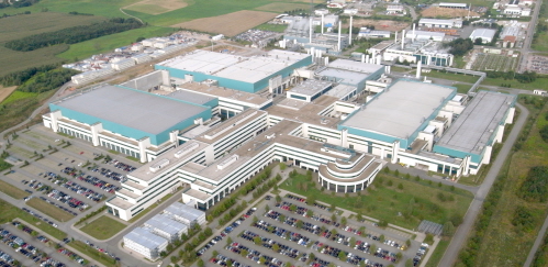
The Dresden Fab 1 with a capacity: 60,000 wafers/month (300 mm)Technology: 45nm to 28nm and now also 22 nm (www.globalfoundries.com)
22FDX leverages the high-volume 28nm platform in GLOBALFOUNDRIES’ state-of-the-art 300mm production line in Dresden, Germany. This technology heralds a new chapter in the “Silicon Saxony” story, building on almost 20 years of sustained investment in Europe’s largest semiconductor fab. GLOBALFOUNDRIES launches its FDX platform in Dresden by investing $250 million for technology development and initial 22FDX capacity. This brings the company’s total investment in Fab 1 to more than $5 billion since 2009. The company plans to make further investments to support additional customer demand. GLOBALFOUNDRIES is partnering with R&D and industry leaders to grow a robust ecosystem and to enable faster time-to-market as well as a comprehensive roadmap for its 22FDX offering.
Full story here: http://globalfoundries.com/newsroom/press-releases/2015/07/13/globalfoundries-launches-industry-s-first-22nm-fd-soi-technology-platform
Furthermore, Rutger Wijburg, senior vice president and general manager of the Dresden Fab 1, acknowledged that Globalfoundries is taking part in European Commission administered projects such as Horizon 2020. "We plan to extend that activity," Wijburg said according to EE Times Europe. As far as I know one of them is WAY-TO-GO CMOS headed by ST Microelectronics
Sunday, July 12, 2015
GLOBALFOUNDRIES Webinar: Extending Moore's Law with FD-SOI Technology
"Extending Moore's Law with FD-SOI Technology" is part of the GLOBALFOUNDRIES Technical Webinar Series. Jamie Schaeffer, Ph.D. explains how FDSOI (Fully Depleted Silicon On Insulator) technology is extending the life of Moore's Law.
Only available by this link : https://www.youtube.com/watch?v=7VmQlpXKtHE#t=100

It has previously been announced this year that Globalfoundries will entry FDSOI at 22 nm and today there will be a press conference in Dresden in front of the Bundeskanslerin Angela Merkels visit to the Dresden Fab tomorrow (Fab 1).


News & Analysis
GlobalFoundries’ FD-SOI Revolution
GRENOBLE, France — The appearance of Gerd Teepe, director and design engineering at GlobalFoundries, at a CEA-Leti-sponsored FD-SOI workshop here has confirmed, once again, rumors surrounding the company’s upcoming “big announcement” about FD-SOI.
Teepe offered, in broad strokes, GlobalFoundries' FD-SOI time schedule. While it was no formal announcement, his presentation implied the company’s oft-leaked but never confirmed big plans in FD-SOI.
Teepe came to Grenoble, ostensibly, to end the suspense.
He said, “We are developing 22nm FD-SOI process technology right now.” The plan is to qualify the process by early 2016 and start volume production by the end of 2016. Asked about what the company’s 22nm FD-SOI process entails, Teepe explained, “We are using STMicroelectronics’ 14nm FD-SOI in our frontend, while using 28nm FD-SOI in the backend.”
[...]
Subscribe to:
Posts (Atom)