Tuesday, July 7, 2015

Photo show from EuroCVD 20 in Sempach

Here all pictures that appear on Twitter (#EuroCVD), Facebook, LinkedIn or that people send me (jonas.sundqvist@baldengineering.com) will be collected!
Main page of Euro CVD 20 : http://eurocvd20.empa.ch/index.html 

Impressions


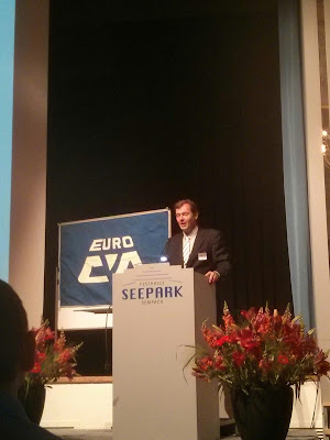
Prof. Hoffman opening the Euro CVD and the famous CVD flag hanging in the background (Photo by Henrik Pedersen)


HERALD Flyers! (Twitter, Henrik Pedersen)


Hoffman and Devi presented HERALD (Twitter, Henrik Pedersen)


Michael Hitchman makes a big announcement: after 20 years, he will retire as the editor of the journal CVD (Twitter, Sean Barry)


Seminars


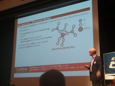
Don´t miss the talk by Henrik Pedersen, Department of Physics, Chemistry and Biology, Linköping University, making an effort to unite us all "A combined ALD-CVD route for group 13 nitride based high frequency devices" Thursday 16 July, 09:30. Here a preview of the talk in the making (Twitter, Henrik Pedersen).


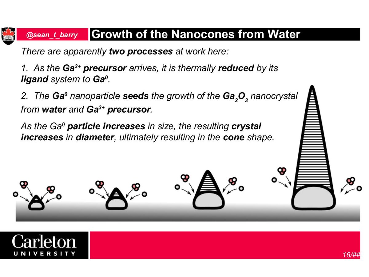
Preview slide from Sean Barry "Growth of Nanocones from Water" (shared on Twitter)


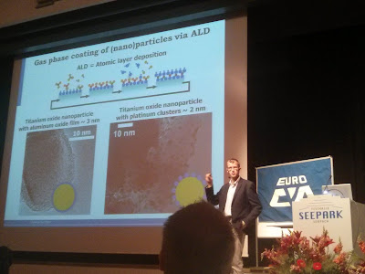
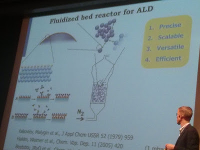
Ruud van Ommen giving his talk on ALD on nano powders using Fluidized bed reactors first publish in Russia 1979 (Photo by Henrik Pedersen)


Talk by Sean Barry on seedless GaO nano wire growth by pulsed CVD (Photo by Henrik Pedersen)


New ketoiminate Y precursors from Devi's group and for yttria stabilized cubic hafnia by ALD and post deposition anneal (Twitter, Henrik Pedersen)


The talk by Prof. Pedersen from Linköping University on combining ALD and CVD for InN (Twitter, Sean Barry)


Ending of Euro CVD Twenty by Prof. Hoffmann (Twitter, Louise)


Poster sessions


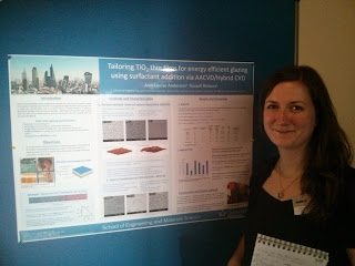
Ann-Louise Andersson at her poster on TiO2 AACVD / Hybrid CVD using surfactants (Photo by Henrik Pedersen)

Trade show


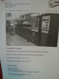
Free Aixtron MOCVD System (Henrik Pedersen)

Dinners and Receptions


Mini golf tournament (Twitter, Russell Binions)


Sightseeing


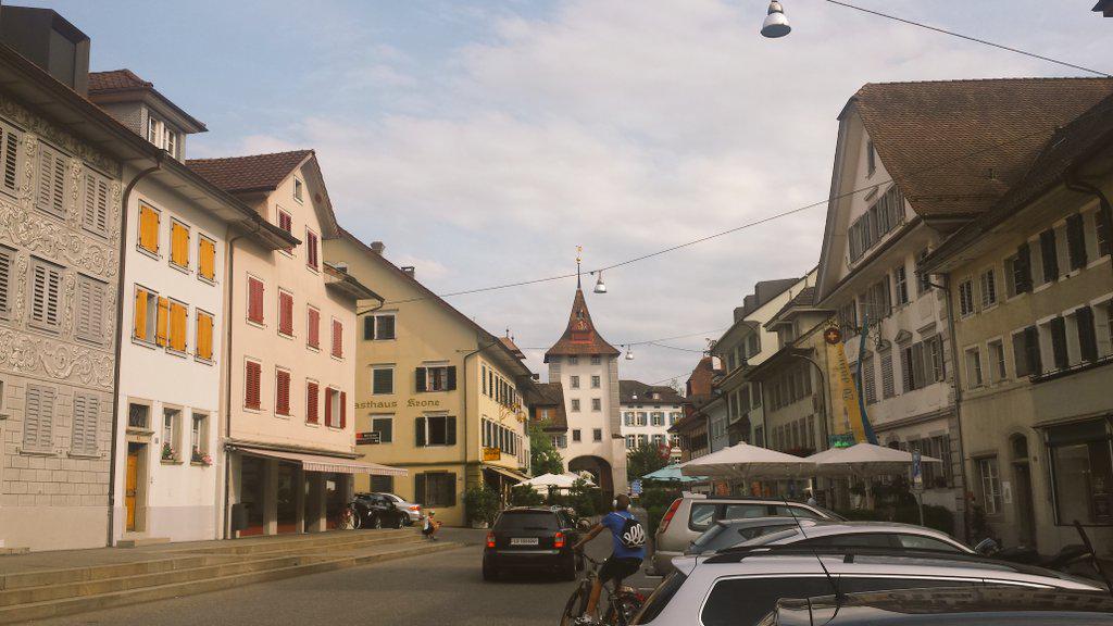
Sempach is a cute little town (Sean Barry, Twitter).


The gathering of ducks in the CVD Duck Pond - Euro CVD!  (Picture by Sean Barry, from Twitter)


A typically Swiss picture (Twitter, Russel BinIons)


Scenic Sempach (Twitter, Sean Barry)


Local gun shop  (Henrik Pedersen)


Boat cruise on the Sempach Lake (Henrik Pedersen)


UPDATE - Atomic Layer Deposition Precursor Suppliers

ALD Pulse has updated the ever growing list of ALD precursor suppliers - the list is reproduced below however for the most up to date version always go here: http://aldpulse.com/chemical-suppliers-view


Air Liquide is a leading supplier of precursors for Atomic Layer Deposition.
Strem is a leading supplier of precursors for Atomic Layer Deposition.
 Praxair is a leading supplier of precursors for Atomic Layer Deposition.
Tanaka is a leading supplier of precursors for Atomic Layer Deposition.
Sigma Aldrich is a leading supplier of precursors for Atomic Layer Deposition.
ATMI  is a leading supplier of precursors for Atomic Layer Deposition.
Nova-Kem is a leading supplier of precursors for Atomic Layer Deposition.
TOSOH is a leading supplier of precursors for Atomic Layer Deposition.
Air Products is a leading supplier of precursors for Atomic Layer Deposition.
Adeka is a leading supplier of precursors for  Atomic Layer Deposition.
Precision Molecular Design Corporation is a leading supplier of precursors for Atomic Layer Depos
DOW Electronic Materials is a leading supplier of precursors for Atomic Layer Deposition
UP Chemical Co; Ltd. is a leading supplier of precursors for Atomic Layer Deposition
EpiValence is a leading supplier of precursors for Atomic Layer Deposition.
Volatec is a leading supplier of precursors for Atomic Layer Deposition.
Pegasus Chemicals is a leading supplier of precursors for Atomic Layer Deposition.
Dock/Chemicals is a leading supplier of precursors for Atomic Layer Deposition.
Ereztech is a leading supplier of precursors for Atomic Layer Deposition.
Gelest is a leading supplier of precursors for Atomic Layer Deposition.
Japan Advanced Chemicals is a leading supplier of precursors for Atomic Layer Deposition.
Seastar Chemicals Inc. is a leading supplier of precursors for Atomic Layer Deposition.

Transparent, Stretchable Conductors Using ALD Nano-Accordion Structure

Whoah! this is really cool stuff" Researchers from North Carolina State University have created stretchable, transparent conductors that work because of the structures’ “nano-accordion” design. The conductors could be used in a wide variety of applications, such as flexible electronics, stretchable displays, or wearable sensors. (Youtube)


The dimensions of each ridge directly affect the transparent conductor’s stretchability (Image: Abhijeet Bagal, NC State News).

The fabrication process of multifunctional nano-accordion structures: 

1. The photoresist template is patterned with 500 nm period using interference lithography.
2. A ZnO thin film is then deposited on the photoresist template using ALD. 
3. The ZnO nano-accordion structure is then transferred by lift-off onto PDMS substrate by dissolving photoresist template.

“We can also control the thickness of the zinc oxide layer, and have done extensive testing with layers ranging from 30 to 70 nanometers thick,” says Erinn Dandley, a Ph.D. student in chemical and biomolecular engineering at NC State and co-author of the paper. “This is important because the thickness of the zinc oxide affects the structure’s optical, electrical and mechanical properties.” - NC State News


A new stretchable, transparent conductor could be used in flexible electronics, stretchable displays, or wearable sensors (Abhijeet Bagal, NCSU News )


Amazing Youtube video showing the trasparent nano-accordion in action.


For all the details to this rather amazing fabrication process check out the article, “Multifunctional Nano-Accordion Structures for Stretchable Transparent Conductors,” is published online in the journal Materials Horizons. The paper was co-authored by Erinn Dandley, Junjie Zhao, Xu Zhang, Christopher Oldham and Gregory Parsons of NC State. The custom ALD reactor used in this work has been described earlier (Chem. Mater., 2009, 21 (5), pp 820–830 DOI: 10.1021/cm8020403)

Monday, July 6, 2015

The oral speakers have been announced for the 13th BALD conference in Tartu

The oral speakers have been announced for the 13th Baltic ALD conference in Tartu, Estonia September 28-29 - congratulations to everybody who made the quite competitive review process for oral presentation!

Invited speakers:

Prof. Markku Leskelä (University of Helsinki, Finland) "Recent challenges of ALD"

Prof. Maarit Karppinen (Aalto University, Finland) "Atomic/molecular layer deposition for multifunctional inorganic-organic thin films"

Prof. Nicola Pinna (Humboldt University of Berlin, Germany) "ALD of metal oxides onto nanostructured carbon materials"

Prof. Christophe Detavernier (University of Gent, Belgium) "Thermal and Plasma Enhanced Atomic Layer Deposition on Powders"

Dr. Massimo Tallarida (ALBA Synchrotron Light Source, Spain) "Recent advances and future directions in the investigation of ALD films with synchrotron radiation"

Dr. Sylwia Gieraltowska (Institute of Physics, Polish Academy of Sciences; Poland) "Oxide thin films grown by atomic layer deposition for antibacterial coatings"

Dr. Karol Fröhlich (Institute of Electrical Engineering, Slovak Academy of Sciences, Slovakia) "Atomic layer deposited films for next generation resistive switching memories"

Oral presentations:

Halit Altuntas "A comparative study of the AlN dielectric films grown by PA-ALD and HCP-ALD" 

Elisa Atosuo "Lithiation of binary oxides using atomic layer deposition and solid state reaction"

Peter Basa "Electrical and optical characterization of Ga-doped ZnO layers adapted for optoelectronics application"

Mikhael Bechelany "Atomic layer deposition: from nanomaterials to membranes applications"

Ole Bethge "Re-growth of GeO2 in between Atomic Layer Deposited high-k oxides and Ge surfaces for improving the interface trap density" 

David Cameron "Spectroscopic ellipsometry of the nucleation of ALD titanium dioxide films."

Bruno Dlubak "Sub-nanometer ALD for Spintronics in Magnetic Tunnel Junctions Based on Graphene Spin-Filtering Membranes"

Stanislaw Dubrovensky "Quantum chemical simulation for the synthesis of monolayer milticomponent coatings using molecular layering technique"

Salvador Duenas "Low temperature resistive switching in Ni-HfO2-Si capacitors"

Simon Elliott "How to design and optimise a process for selective area ALD" 

Michael Getz "Down Conversion in YbVO4 and YVO4:Yb3+, Eu3+ Thin Films Synthesized by Atomic Layer Deposition"

Carlos Guerra "Morphology and Crystallinity Control of Ultrathin TiO2 Layers Deposited on Carbon Nanotubes by Temperature-Step ALD"

Christoph Hossbach "Compact Plasma Source for Direct and Remote Plasma Enhanced Atomic Layer Deposition of Conductive Thin Films"

Alexander G. Hufnagel "Nanostructured AZO supports for photoelectrochemical water-splitting by atomic layer deposition and hydrothermal methods"

Taivo Jõgiaas "Mechanical properties of aluminium, zirconium, hafnium and tantalum oxides and their nanolaminates grown by atomic layer deposition"

Marianna Kemell "Atomic layer deposition of As2S3 thin films" 

Erwin Kessels "Nanotailoring ZnO:X (X = Al, B) Films by Atomic Layer Deposition" 

Peter King "Interface engineering with ALD on germanium"

Harm Knoops "Low temperature plasma-assisted ALD of conductive films" 

Kristian Blindheim Lausund "Deposition of organic-inorganic hybrid films of Zr-1,4-BDC by ALD"

Anatoly Malygin ""Framework" hypothesis of V. B. Aleskovskii - the fundamental basis of the molecular layering method"

Janne-Petteri Niemelä "Transport properties of ALD-fabricated Nb-doped TiO2 thin films" 

Matti Putkonen "Antimicrobial properties of ALD films" 

Riikka Puurunen "Mechanical property mapping of ALD thin films" 

Erwan Rauwel "ALD Applied to Conformal Rare-Earth Coating of Oxide Nanoparticles for Low Temperature Thermal Imaging Applications" 

Väino Sammelselg "ALD for advanced anti-corrosion nanocoatings"

Lionel Santinacci "Atomic layer deposition of Pd nanoparticles on TiO2 nanotubes for electrocatalytic oxidation of ethanol: effect of the substrate"

Uwe Schroeder "Piezo- and Ferroelectric Properties of ALD HfO2 Based Nanolaminates"

Sanni Seppälä "Effect of Oxygen Source on Film Properties in ALD of Lanthanum Oxide"

Imre Miklós Szilágy "Photocatalytic properties of crystalline and amorphous ALD TiO2 thin films"

Andy Thomas "Atomic layer deposited HfO2-based magnetic tunnel junctions"

Tobias Törndahl "An all atomic layer deposition window layer structure for increased photocurrent generation in CIGS solar cells"

Silvia Vangelista "Atomic layer- and chemical vapor- deposition of multiferroic Er-Fe-O thin films"

Timo Vähä-Ojala "Modelling of carrier gas flow in ALD reactor"

Katja Väyrynen "Photo-ALD of Tantalum and Niobium Oxides"

Christoph Wiegand "Characterization of ALD grown GaxSb2-xTe3 thin films: Halosilylation based reactions for controlling the transport properties"

Claudia Wiemer "Effect of the atomic layer deposition process on the crystallization properties of Al2O3."

Ana Zuzuarregui "Highly efficient encapsulation of organic opto-electronic devices utilizing ALD"

ALD in nanostructured photovoltaics by Stanford University

Atomic layer deposition in nanostructured photovoltaics: tuning optical, electronic and surface properties

Axel F. Palmstrom, Pralay K. Santra and Stacey F. Bent
Nanoscale, 2015, Advance Article DOI: 10.1039/C5NR02080H


Nanostructured materials offer key advantages for third-generation photovoltaics, such as the ability to achieve high optical absorption together with enhanced charge carrier collection using low cost components. However, the extensive interfacial areas in nanostructured photovoltaic devices can cause high recombination rates and a high density of surface electronic states. In this feature article, we provide a brief review of some nanostructured photovoltaic technologies including dye-sensitized, quantum dot sensitized and colloidal quantum dot solar cells. We then introduce the technique of atomic layer deposition (ALD), which is a vapor phase deposition method using a sequence of self-limiting surface reaction steps to grow thin, uniform and conformal films. We discuss how ALD has established itself as a promising tool for addressing different aspects of nanostructured photovoltaics. Examples include the use of ALD to synthesize absorber materials for both quantum dot and plasmonic solar cells, to grow barrier layers for dye and quantum dot sensitized solar cells, and to infiltrate coatings into colloidal quantum dot solar cell to improve charge carrier mobilities as well as stability. We also provide an example of monolayer surface modification in which adsorbed ligand molecules on quantum dots are used to tune the band structure of colloidal quantum dot solar cells for improved charge collection. Finally, we comment on the present challenges and future outlook of the use of ALD for nanostructured photovoltaics.


Air Products and SNU present low temperature ALD process for GST for PCRAM

Phase change random access memory (PCRAM) is one of the promising next-generation memory technologies because of its nonvolatile data retention property and rapid writing and reading speeds. Air Product and Seoul National University (SNU) now presents a stable and reliable  conformal ALDprocess for depositing the challenging GST material at low temperature. The Gb–Sb–Te films were deposited using a 200 mm shower head type ALD reactor from Quros (CN-1, Plus-200).

Combined Ligand Exchange and Substitution Reactions in Atomic Layer Deposition of Conformal Ge2Sb2Te5 Film for Phase Change Memory Application


Taeyong Eom, Taehong Gwon, Sijung Yoo, Byung Joon Choi, Moo-Sung Kim, Iain Buchanan, Sergei Ivanov, Manchao Xiao, and Cheol Seong Hwang
 

For phase change memories application, Ge–Sb–Te films were prepared by a stable and reliable atomic layer deposition (ALD) method. Ge(OC2H5)4, Sb(OC2H5)3, [(CH3)3Si]3Sb, and [(CH3)3Si]2Te were used to deposit various layers with compositions that can be described by combinations of GeTe2–Sb2Te layers including Ge2Sb2Te5 at a substrate temperature as low as 70 °C. A shift in composition of Sb–Te films from Sb2Te3 to Sb2Te composition was achieved by combining ligand exchange and substitution reaction between Sb in [(CH3)3Si]3Sb and Te in the Sb2Te3 layer. This surface-limited ALD process allowed highly conformal, smooth, and reproducible film growth over a contact hole structure, highlighting the feasibility of phase change memory applications.

Sunday, July 5, 2015

University of Wisconsin Madison demonstrate biodegradable microwave flexible TFTs

University of Wisconsin Madison demonstrate microwave flexible TFTs built on a cellulose nanofibrillated fiber (CNF) substrate by employing transferrable single crystalline Si nanomembranes (Si NMs)


(a) Illustration of the degradable  (b) Microscopic image of a finished device on the CNF substrate. (c) An optical image showing the transparency and flexibility of the CNF substrate. (d) An optical image and (e) an enlarged optical image showing the biodegradability of the array of devices built on the CNF substrate: (left) as-made and (right) after 3 weeks degradation.
Citation: Appl. Phys. Lett. 106, 262101 (2015); http://dx.doi.org/10.1063/1.4921077

Microwave flexible transistors on cellulose nanofibrillated fiber substrates


Jung-Hun Seo, Tzu-Hsuan Chang, Jaeseong Lee, Ronald Sabo, Weidong Zhou, Zhiyong Cai, Shaoqin Gong and Zhenqiang Ma

Appl. Phys. Lett. 106, 262101 (2015); http://dx.doi.org/10.1063/1.4921077

In this paper, we demonstrate microwave flexible thin-film transistors (TFTs) on biodegradablesubstrates towards potential green portable devices. The combination of cellulose nanofibrillated fiber (CNF) substrate, which is a biobased and biodegradable platform, with transferrable single crystalline Si nanomembrane (Si NM), enables the realization of truly biodegradable, flexible, and high performance devices. Double-gate flexible Si NM TFTs built on a CNF substrate have shown an electron mobility of 160 cm2/V·s and f T and f max of 4.9 GHz and 10.6 GHz, respectively. This demonstration proves the microwave frequency capability and, considering today's wide spread use of wireless devices, thus indicates the much wider utility of CNF substrates than that has been demonstrated before. The demonstration may also pave the way toward portable green devices that would generate less persistent waste and save more valuable resources.


Friday, July 3, 2015

UPDATED - 2014 PEALD Year in Review

The Plasma ALD Guy has updated his 2014 PEALD Year in Review : http://plasma-ald.com/2014YIR/2014YIR.php and republished below.

"To date, I have tracked down 131 publications using PEALD films accepted for publication during 2014. There are probably others I have not yet come across. Papers in which the focus is the development of PEALD films tend to be quite easy to track down. When PEALD is just one of the techniques utilized for some new application, finding the paper can be challenging, especially when few processing details are offered at which to point a search engine. Identifying these publications may be more challenging, but it is fun when I do find them and it is great to see the breadth of applications for which PEALD films are being utilized."

2014 PEALD Publications by Month

2014 PEALD Films

2014 PEALD Hardware

2014 PEALD Locations

Thursday, July 2, 2015

Picosun and Carleton Strike Gold with ALD


Picosun Oy, the leading provider of high quality Atomic Layer Deposition (ALD) solutions for industrial manufacturing, and Carleton University, Canada, report uniform ALD gold deposition on complete silicon wafers. The gold films were prepared using PICOSUN™ plasma ALD tool and a new gold precursor developed by Prof. Seán Barry. The novel process was described in the talk given at the AVS 15th ALD meeting held in Portland, USA.


Gold is a highly sought-after material in today's microelectronics, optoelectronics, and microsystems manufacturing. Due to its excellent chemical inertness and high thermal and electrical conductivity it has a plethora of applications for example in 3D packaging (via interconnects), wafer metallization, and heat dissipation of IC components, and preparation of electrical connections, structural layers, and electrodes for MEMS devices.

"We have worked on gold metal deposition chemistry for a few years now, and this process is a breakthrough. Our PICOSUN™ ALD system handles a wide variety of precursors beautifully, and its ease of use has made process development for challenging materials much easier. The uniformity that we are able to achieve with the PICOSUN™ plasma ALD tool is very impressive," states Seán Barry, Associate Professor of the Department of Chemistry, Carleton University, Ottawa, Canada.

"We are excited about these recent advances in gold deposition by ALD. Picosun's plasma ALD technology is optimal for metal deposition. This has enabled gold manufacturing also before, but the now published, larger scale results will definitely catch the interest of a vast number of our production customers in IC, MEMS, and electronics industries," summarizes Dr. Wei-Min Li, Applications Director of Picosun.

Picosun provides the most advanced ALD thin film technology and enables the industrial leap into the future by novel, cutting-edge coating solutions, with four decades of continuous expertise in the field. Today, PICOSUN™ ALD systems are in daily production use in numerous major industries around the world. Picosun is based in Finland, with subsidiaries in USA, China, Taiwan, and Singapore, and a world-wide sales and support network.

Located in the nation's capital, Carleton University is a dynamic research and teaching institution with a tradition of leading change. Its internationally recognized faculty, staff and researchers provide more than 27,000 full- and part-time students from every province and more than 100 countries around the world with academic opportunities. Carleton's creative, interdisciplinary and international approach to research has led to many significant discoveries and creative works in science and technology, business, governance, public policy and the arts. As an innovative institution, Carleton is uniquely committed to developing solutions to real-world problems.

Wednesday, July 1, 2015

Leading Edge Embedded NVM Workshop September 28-30 at Centre Microélectronique de Provence

The "Leading Edge Embedded NVM Workshop" (e-NVM), with the support of "l'Ecole Nationale Supérieur des Mines de Saint-Etienne", is organized by ARCSIS, a trade association for the microelectronics and semiconductor activities in the Provence-Alpes-Riviera (PACA) region, in France. ARCSIS participates in assuring sustainability, full economic development and enhanced competitiveness of the regional microelectronics and communicating objects industry.


Further to the success of the second edition of the «Leading-edge Embedded Non Volatile Memories» workshop in 2013 with over 180 international participants, ARCSIS reiterates the event in 2015 at the «Centre Microélectronique de Provence» in Gardanne (Aix-en-Provence area, France). The third edition of this workshop dedicated to embedded non-volatile memories takes place from 28 to 30 of September 2015.

The aim of the Workshop is to bring together researchers and industrials of both sides of the chain around Embedded Non-Volatile Memories: designers and manufacturers on the one hand and contractors and end-users on the other hand.

Worldwide specialists in research and industry of Embedded NVM domain have participated in e-NVM: Altis Semiconductor, Applied Materials, ASM International, ATMEL, CEA-LETI-MINATEC, CEA-Liten, Crocus Technology, Cypress Semiconductor, ELMOS Semiconductor AG, EMSE / CMP, EM Microelectronics (Swatch), Gemalto, Globalfoundries, Grace Semiconductor, IMEC, IM2NP Aix –Marseille University, Infineon Technologies AG, Inside Secure, Institut des Matériaux de Nantes, Institut Supérieur d’Electronique de Paris, LIRMM, Molecular Electronics Research Institute (MERI JSC), Nantero, NXP Semiconductors, Oerlikon Systems, Polytech’Nice, Rambus, Robert Bosch Gmbh, Samsung Electronics Co. Ltd, Starchip, STMicroelectronics, Università di Modena e Reggio Emilia, X-FAB Semiconductor Foundries AG...

Some companies and laboratories have already confirmed their participation as invited speakers: 

Aix-Marseille University-IM2NP (France) - Vincenzo Della Marca
CEA-LETI (France) - Bastien Giraud
CEA-Leti and IM2NP (France) - Alexandre Levisse
CEA, LETI, MINATEC Campus (France) - Gabriele Navarro
CEA-SACLAY (France) - Christian Gamrat
Crocus/LIRMM (France) - Sophiane Senni
Crossbar (USA) - Sylvain Dubois
Cypress Spansion (USA) - Igor Kouznetsov
Forschungszentrum Juelich GmbH (Germany) - Dr Vikas Rana
GLOBALFOUNDRIES Europe (Germany) - Robert Meier
Grace Semiconductor (China) - Weiran Kong
IM2NP (France) - Damien Deleruyelle
Inside Secure (France) - Laurent Sustek
Integrated System Solution Inc. (USA) - Julian Chang
Kilopass (USA) - André Hassan
Macronix (Taiwan) - Jocelyn Carroue
Panasonic (Japan) - Takumi Mikawa
Politecnico di Torino (Italy) - Elena Ioana Vatajelu
Rhealtys (France) - Jean-Pierre Delesse
Safran/Morpho (France) - Nicolas Prawitz
Samsung (Korea) - Jisung Kim
SMIC (China) - Jay Ning
SST-Microchip (USA) - Alex Kotov
SST-Microchip (USA) - Nhan Do
Starchip (France) - Speaker to be confirmed
STMicroelectronics – MMS Group (Italy) - Antonino Conte

Kurt J. Lesker introduces new R&D Platform for organic material deposition, ALD and PEALD

Kurt J.Lesker's most affordable organic material deposition system platform, designed specifically with the entry to mid-level user in mind. Standard configurations compatible with up to 100mm x 100mm square or 150mm diameter substrates, up to 350°C heating and cooling, glove box option available.


  • Designed to accommodate specific organic and inorganic thin film applications such as, OLED Displays, Lighting, Organic Photovoltaics and Electronics.
  • Offers both organic and metal deposition capabilities in a single chamber.
  • Recipe driven computer system control with data logging option available.
  • Field tested and proven design.

Glovebox Interfaced System: Incorporates a sliding front door with glove box interface flange and sliding rear door for unobstructed chamber access. Facilitates thermal and plasma enhanced atomic layer deposition techniques

Standard chambers are configured to allow up to:

(12) 1cc, 10cc, or 35cc plug-in low-temperature organic sources

(4) Thermal evaporation sources and pellet feeder option

- Personalised combinations available based on system platform

- Scroll type rough pumping; cryogenic high vacuum pumping

- Standard configurations compatible with up to 8" x 8" (200mm x 200mm) square substrates, up to 350°C heating, glove box, up to five mask storage shelves with motorised transfer, and wedge tool options

- Basic computer control with recipe and data logging options are available as well

Fraunhofer Center for Nanoelectronic Technologies Installs 200mm PEALD FlexAL Tool

The Fraunhofer IPMS  in Dresden, Germany has installed a FlexAL system for plasma enhanced and thermal ALD from Oxford Instruments Plasma Technology in its Center for Nanoelectronic Technologies.


The fields of use for the new tool are research and development on processes for metal oxides for ultra-thin integrated 3D capacitors, the development of new and unique metal ALD processes, and as a platform with a combinatorial screening concept including in-situ metrology and standardised tests for ALD/PEALD precursor development serving gas and chemical supplying companies. Additionally the FlexAL will serve as a 200mm PEALD tool for the MOEMS pilot line at the Fraunhofer IPMS.


The Center for Nanoelectronic Technologies has a long-term experience in atomic layer deposition (ALD), which is a sophisticated process where monolayer after monolayer is built up. ALD is the process of choice whenever precise thickness and composition control of thin films in the nanometer range are required. This is particularly the case for semiconductor devices where the smallest dimensions of some tens of nanometer are fabricated, and an increasing demand is observed for high conformal thin ALD films. Consequently, the development of materials and compounds deposited by ALD increases impressively.

After a rigid tendering process the Oxford Instruments FlexAL PEALD system was chosen because of its capabilities as a high end ALD research and development tool. The broad range of processes enabled by the FlexAL’s design allows the combination of plasma and thermal processes in one fully automated recipe as well as the flexible precursor cabinet which enables effective combinatorial precursor screening with in-situ metrology.

“The proven performance and versatility of the Oxford Instruments FlexAL together with the availability of multiple room temperature variants of PEALD processes made it the ‘system of choice’ for the Center for Nanoelectronic Technologies. We are extremely pleased to be supplying this prestigious research institute with this,” says Dr. David Haynes, Sales, Service and Marketing Director, Oxford Instruments Plasma Technology.