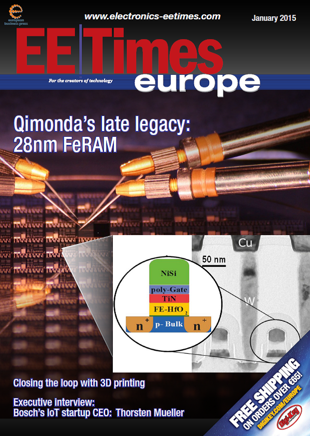
Friday, March 27, 2015

UPDATED - Workshop on Fundamentals of ALD - June 8 & 9, Eindhoven

Cost Action "HERALD" workshop on Fundamentals of ALD - June 8 & 9, Eindhoven

Organized by Erwin Kessels Professor in Applied Physics at Eindhoven University of Technology. June 8 (start at noon) to June 9 (end mid-afternoon). Please see http://www.nanomanufacturing.nl/

"The aim of the workshop is to spark a discussion about current topics in the field of atomic layer deposition (ALD) by addressing fundamental aspects of the method. It is expected that this discussion will lead to new and refined insights beneficial to further advance the field of ALD. The aim is to serve both scientists who work at the forefront of ALD research as well as newcomers and technologists who want to get a better understanding of ALD."

"Consistent with the aim of the event, this will be a "true" workshop in which participants are encouraged to actively take part in the presentations and discussions. During the workshop, 5 current topics within the field of ALD will be covered with ample time and opportunity for discussion and interaction. Each topic will be introduced by speaker who is an authority in the field. In the introduction, basic aspects will be presented such that non-experts can take part in the discussion while the leading edge of the current understanding will also be presented. Afterwards, a specific case will be addressed in more detail by a researcher who has studied an aspect of the specific topic in depth. This will be followed by presentations from the participants and an open discussion."
venue

Nanomanufacturing: ALD FUNdamentals nanomanufacturing.nl Dates: June 8 & 9 Location: Eindhoven, NL The aim of the workshop is to spark a discussion about current topics in the field of atomic layer deposition (ALD) by addressing fundamental aspects of the method. It is expected that this discussion.
    Speakers:
    • Dr. Chaitanya Ande (Eindhoven University of Technology, NL)
    • Ir. Roger Bosch (Eindhoven University of Technology, NL)
    • Prof. dr. ir. Erwin Kessels (Eindhoven University of Technology, NL)
    • Dr. ir. Harm Knoops (Oxford Instruments, NL)
    • Dr. ir. Adrie Mackus (Stanford University, USA)
    • Dr. Paul Poodt (Holst Centre / TNO, NL)
    • Dr. Stephen Potts (Queen Mary University of London, UK)
    • Ir. Vincent Vandalon (Eindhoven University of Technology, NL)
    • Angel Yanguas-Gil, PhD (Argonne National Laboratory & Northwestern University, USA)
    • ...
    Discussion Leaders
    • Low temperature ALD – Suvi Haukka (ASM Microchemistry)
    • ALD of nitrides– Riikka Puurunen (VTT Technical Research Centre of Finland)
    • ALD of metals – Simon Rushworth (EpiValence)
    • ALD of multi-element oxides – Chris Hodson (Oxford Instruments Plasma Technology)
    • Spatial ALD vs Temporal ALD – Dennis Hausmann (Lam Research)

    Program

    Important dates

    • March 27 - Workshop Announcement
    • April 20 - Detailed program announced
    • May 1 Deadline for requesting travel support
    • May 29 - Submission deadline for short presentations
    • May 29 - Deadline for registration
    • June 8 & 9 - Workshop!

    Topics

    The following topics will be addressed during the workshop:
    Available soon: Click on the topics for a more detailed description and submission guidelines on how to contribute to the session.
    How to participate?

    You can participate actively in the session about low-temperature ALD by giving a short presentation or a pitch after the two presentations that are already scheduled. Please submit a short presentation clearly describing the observation, issue or open question that you would like to discuss to contact@nanomanufacturing.nl. We would like to receive your presentation before the 29th of May, which will allow sufficient time for us to evaluate your contribution. You might receive suggestions from the session coordinators to fit it in better in the session.

    If your short-talk is accepted, you can chose to bring a poster in addition to giving the short talk. The poster will receive attention during the breaks and during lunch. The poster will allow you to present more background information and interesting findings which cannot be discussed during the sessions due to time constraints.


      Too many good questions and discussions to tweet during the ALD Fundamentals workshop. It was a lot of FUN!

      Stanford GaAs process could yield better solar cells, faster chips

      New Stanford manufacturing process could yield better solar cells, faster chips
      Silicon isn't the only chip-making material under the sun, just the cheapest. But a new process could make the alternative material, gallium arsenide, more cost effective.

      http://www.dataversity.net/wp-content/uploads/2014/06/Stanford-University-logo.jpg

      Silicon is typically used in solar cells and computer chips. Gallium arsenide is an alternative material with many advantages. But it costs too much. A new process would reduce manufacturing costs.

      "Solar cells that use gallium arsenide hold the record when it comes to the efficiency at which they convert sunlight into electricity," said Bruce Clemens, the professor of materials science and engineering who led this work.

      "Once it becomes possible to make gallium arsenide more cost-effectively, other people will jump in to improve other parts of the process,'' Clemens said. "And with each advance, more uses will open up, especially in solar energy generation where gallium arsenide has clear efficiency advantages."

      Micron and Intel Unveils 3D NAND

      Micron and Intel Unveils 3D NAND : The World’s Highest-Capacity NAND Flash Memory


      "The interdependent, growing demands of mobile computing and data centers continue to drive the need for high-capacity, high-performance NAND flash technology. With planar NAND nearing its practical scaling limits, delivering to those requirements has become more difficult with each generation. Enter our new 3D NAND technology, which uses an innovative process architecture to provide 3X the capacity of planar NAND technologies while providing better performance and reliability."


      3 times the capacity of existing NAND products—enough to enable 3.5TB gum stick-sized SSDs or more than 10TB in standard 2.5-inch SSDs.
       
      Bildergebnis für intel logo


      Tuesday, March 24, 2015

      Nanoplas’ atomic-layer downstream etching (ALDE) technology explained


      Nanoplas
       
      Nanoplas’ atomic-layer downstream etching (ALDE) technology enables a new class of plasma-based etching and stripping processes that may be used at the 14nm technology node and beyond. Here is a new video that was released recently explaining the technology:

      LAM Research - Multiple Patterning Makes Miniaturization Possible

      Here is a great blog on Multiple Patterning by LAM Research that explains it all in a straight forward way. The main technologies are pictured below - check ot the blog for details.

      https://firmenportal.iaeste.at/sites/default/files/logos/492-Lam%20Research/Lam_Research_logo_color%20june.jpg
       
      "Today’s advanced chip designs have smaller and more dense features than can be created using available lithography capability. Fortunately, advanced patterning techniques have been devised to work around these limitations by using multiple patterns of larger dimensions to obtain smaller and/or more tightly packed features."

      (1) Convential (Single) Patterning

       
      In conventional lithography, a wafer is coated with a light-sensitive material called photoresist. Light is then streamed through a photomask (a pattern of transparent and opaque areas), exposing the photoresist in some places, but not in others. The exposed regions are then etched away, while covered areas remain protected (in the case of positive photoresist). The end result is a set of features whose size and density are determined by the original photoresist pattern.

      (2) Double Patterning 

       
      One of the most widely adopted double patterning schemes is double exposure/double etch, also known as litho-etch-litho-etch, or LELE.

      (3) The Self-Aligned Spacer Technique - Self-Aligned Double Patterning (SADP)


      Examples of self-aligned double patterning (SADP) applications include formation of fins in FinFET technology, lines and spaces for interconnect levels, and bitline/wordline features in memory devices

      (4) Multiple Patterning - Self-Aligned Quadruple Patterning (SAQP)


      Self-aligned quadruple patterning (SAQP) can achieve a half-pitch resolution of ~10 nm


      Check out this awesome video to understand Atomic Layer Deposition (ALD) and Atomic Layer Etching (ALE), which are two very important processes for driving nano-patterning and scaling further down to below 10 nm.


      Monday, March 23, 2015

      Picosun and NCTU Launch Industrial ALD Facility in Taiwan

      National Chiao Tung University (NCTU), Taiwan, and Picosun Oy, the leading provider of high quality Atomic Layer Deposition (ALD) solutions for global industries, establish a Joint Industrial ALD Research Laboratory at the premises of X-Photonics Interdisciplinary Center at NCTU to enable the next generation of micro- and optoelectronics using ALD technology.

      http://life.nctu.edu.tw/~jwchu/wp-content/uploads/2013/10/NCTU.png


      With this collaboration NCTU and Picosun will develop a wide range of interdisciplinary technology solutions for applications such as microelectronic devices for: 
       
      • 7 nm technology node
      • high-brightness light emitting diodes (HBLED)
      • high electron mobility transistors (HEMT)
       
      Both fundamental research and advanced device fabrication for industrial applications will be the core objectives of the Joint Industrial ALD Research Laboratory.

      Picosun Oy Logo / Picosun Oy Logo

      "It's obvious that Picosun, with their world-leading experience in ALD system design and process knowhow, has been chosen as our ALD technology provider. We are happy and excited to start this collaboration to realize a whole new generation of micro- and optoelectronic products. Based on the energy of NCTU in the semiconductor field, I think we will achieve lots of success in the near future," summarizes Professor Hao-Chung Kuo, Associate VP of NCTU, and both IEEE and OSA fellow.

      "Taiwan is one of the world's leading semiconductor manufacturing hubs. Picosun's state-of-the-art ALD technology is a key enabler for advanced micro- and optoelectronics fabrication. Establishing a partnership and a joint research laboratory with NCTU will provide our existing and future industry customers not only local access to our technology for their applications, but also stronger collaboration ties for future generation products enabled by our ALD technology. This is further supported by our newest subsidiary, Picosun Taiwan, which was established two months ago," states Dr. Wei-Min Li, CEO of Picosun Asia and Applications Director of Picosun Group.

      Picosun provides the most advanced ALD thin film technology and enables the industrial leap into the future by novel, cutting-edge coating solutions, with four decades of continuous expertise in the field. Today, PICOSUN™ ALD systems are in daily production use in numerous major industries around the world. Picosun is based in Finland, with subsidiaries in USA, China, Taiwan, and Singapore, and a world-wide sales and support network.

      Sunday, March 22, 2015

      Ferroelectric HfO2 Based Materials and Devices: Current Status and Future Prospects

      Ferroelectric Hafnium Oxide Based Materials and Devices: Assessment of Current Status and Future Prospects [OPEN ACCESS]

      J. Müller, P. Polakowski, S. Mueller and T. Mikolajick
      ECS J. Solid State Sci. Technol. volume 4, issue 5, N30-N35

      Abstract

      Bound to complex perovskite systems, ferroelectric random access memory (FRAM) suffers from limited CMOS-compatibility and faces severe scaling issues in today's and future technology nodes. Nevertheless, compared to its current-driven non-volatile memory contenders, the field-driven FRAM excels in terms of low voltage operation and power consumption and therewith has managed to claim embedded as well as stand-alone niche markets. However, in order to overcome this restricted field of application, a material innovation is needed. With the ability to engineer ferroelectricity in HfO2, a high-k dielectric well established in memory and logic devices, a new material choice for improved manufacturability and scalability of future 1T and 1T-1C ferroelectric memories has emerged. This paper reviews the recent progress in this emerging field and critically assesses its current and future potential. Suitable memory concepts as well as new applications will be proposed accordingly. Moreover, an empirical description of the ferroelectric stabilization in HfO2 will be given, from which additional dopants as well as alternative stabilization mechanism for this phenomenon can be derived. 

      Figure 4.

      Comparison of the two major flavors of FRAM. 1T-1C: (a) Working principle illustrating the sensing margin / switched polarization Psw derived from switched charge Qsw and non-switched polarization Pnsw in the P-E-hysteresis. (b) DRAM-like architecture of FRAM adding a plateline to word- and bitline for bipolar ferroelectric switching. (c) TEM-micrograph and related P-E-hysteresis of a FE-HfO2 based deep trench capacitor array proving the concept of 3D-integration capability. To illustrate the advantage of this area enhancement, the polarization density is calculated with respect to the lateral footprint of a comparable planar capacitor. 1T: (d) Illustration of the working principle by a graphical representation of the charge neutrality condition in a MFIS stack. Position 1 and 2 of the insulator-semiconductor loadline represents the transition from the ON-state to the OFF-state of the FeFET or vice versa. Accordingly, the gate voltage difference to turn on/off the FeFET can be approximated by 2 · VC = 2 · Ec · dFE, i.e. the memory window MW. (e) Disturb resilient AND architecture of the FeFET. (f) TEM-micrograph and related ID-VG-hysteresis of a FE-HfO2 based 28 nm high-k metal gate transistors proving the concept of advanced 1T FRAM scalability

      The recent success of smartphones and tablet computers has accelerated the R&D of fast and energy efficient non-volatile semiconductor memories, capable of replacing the conventional SRAM-DRAM-Flash memory hierarchy. These so called emerging memories usually leverage on the fact that certain materials possess the capacity for remembering their electric, magnetic or caloric history. For the extensively investigated ferroelectrics this ability to memorize manifests in atomic dipoles switchable in an external electric field. This unique property renders them the perfect electric switch for semiconductor memories. Consequently, only a few years after the realization of a working transistor the first ferroelectric memory concepts were proposed.

      However, more than 60 years and several iterations later it is now clear that the success or failure of FRAM is mainly determined by the proper choice and engineering of the ferroelectric material. Perovskite ferroelectrics and related electrode systems underwent an extensive optimization process to meet the requirements of CMOS integration and are now considered the front up solution in FRAM manufacturing. Nevertheless, those perovskite systems require complex integration schemes and pose scaling limitations on 1T and 1T-1C memory cells that until now remain unsolved. This creates an unbalance between memory performance on the one side and manufacturing and R&D costs on the other side. This dilemma has ever since restricted FRAM to niche markets. 

      With the recent demonstration of ferroelectricity in HfO2-based systems (FE-HfO2) a CMOS-compatible, highly scalable and manufacturable contender has emerged, that significantly expands the material choice for 1T and 1T-1C ferroelectric memory solutions as well as nanoscale ferroelectric devices. 

      In this paper we will review and expand the current understanding of ferroelectricity in HfO2, as well as discuss future prospects of ferroelectric HfO2-based devices with respect to scaling, reliability and manufacturability. Opportunities and drawbacks of this disruptive development in ferroelectric material science will be critically examined. 

      Continue reading in the full paper with Open Access here.

      Saturday, March 21, 2015

      Highly Selective Directional ALE of Silicon by LAM Research (OPEN ACCESS ARTICLE)

      LAM Research, Intel and others are pumping out great publications on Atomic Layer Etching (ALE) at the moment. Here is a good one on Si etchning from LAM Reasearch and I think this is also the first time I come across the term EPC as in "Etching per Cycle" as corresponding to GPC "Growth per Cycle" in ALD. Also the concept of an ALE window is explained. Check out the abstract below or go for the complete article by following the link:

      Highly Selective Directional Atomic Layer Etching of Silicon (OPEN ACCESS)
      Samantha Tan, Wenbing Yang, Keren J. Kanarik, Thorsten Lill, Vahid Vahedi, Jeff Marks and Richard A. Gottscho
      Abstract
      Following Moore's Law, feature dimensions will soon reach dimensions on an atomic scale. For the most advanced structures, conventional plasma etch processes are unable to meet the requirement of atomic scale fidelity. The breakthrough that is needed can be found in atomic layer etching or ALE, where greater control can be achieved by separating out the reaction steps. In this paper, we study selective, directional ALE of silicon using plasma assisted chlorine adsorption, specifically selectivities to bulk silicon oxide as well as thin gate oxide. Possible selectivity mechanisms will be discussed. 

      As the IC industry approaches sub 10 nm devices, the need for atomic scale fidelity has been recognized. In the field of deposition, atomic layer deposition (ALD) emerged. The driving forces for advancement of ALD were among others conformal deposition in high aspect ratio structures and deposition of dielectrics and metals with atomic layer control. The idea that an analogous technology for removal of material might exist was proposed over 10 years after the discovery of ALD. The number of publications on this so called atomic layer etch (ALE) increased significantly in recent years and now ALE is transitioning from the lab to the fab.

      One highly desirable quality of ALE is selectivity. Recently, Hudson et al. verified that a directional oxide ALE process can etch SiO2 selective to Si3N4. Ikeda et al. showed that thermal ALE of germanium can be selective to silicon or SiGe. Thermal etching is isotropic and not directional. Etching of 3D devices requires directionality and selectivity. FinFET gate etching for instance requires overetches of 40 nm and more to clear the silicon between the fins while gate oxide is exposed. As fin heights increase to achieve the required Ion currents while CD's are shrinking further, the amount of overetch is expected to increase even more. During extended plasma exposure, species from the plasma can penetrate into the fin silicon and cause lattice damage and undesired fin recess. This drives the need for new etching approaches such as ALE. 

      ALE processes are comprised of single unit steps which repeat in cycles. These single unit steps use the simplest possible chemistry to realize specific surface processes such as activation and removal. In analogy to ALD, ALE single unit steps should have as much self-limitation as possible. Self-limitation or saturation eliminates the influence of transport phenomena which are the root cause of aspect ratio dependent etching or ARDE on a microscopic scale.8 On an atomic scale, saturation of the single unit steps should lead to atomic level smoothness of the etching surface.5

      Another important concept which can be adapted from ALD is the existence of an ideal process window. Figure 1a illustrates the so called “ideal ALD window,” which is defined as the region of nearly ideal ALD behavior between non-ideal regions.3 The graph shows “growth per cycle” or GPC as a function of surface temperature which for chemical surface reactions represents the available energy to overcome reaction barriers. The analogy of an ideal process window for ALE with ion based removal is shown in Fig. 1b. Here, “etch per cycle” or EPC is shown as a function of ion energy. The material to be etched is activated in a first step and the activated layer is removed in a second step by energetic ions. For instance, silicon can be activated by chlorine molecules or radicals and the resulting surface layer of SiClx can be removed by low energy noble gas ions. This particular embodiment of ALE is directional since the removal step is directional due to the use of ions that have been accelerated by a plasma sheath or ion beam source. There are other embodiments of ALE as well. For instance, in the absence of directionality in both, the activation and removal step, the result is isotropic ALE. In this case, surface temperature can be used as control variable of the removal step.


      Figure 1.

      Fig. 1. a. Ideal process window for ALD adapted from. Ref. 3 b. Ideal process window for direction ALE. The region called “incomplete removal” in Figure 1b is characterized by ion energies that are insufficient to completely remove the activated surface layer. Under the conditions labeled “ideal ALE window,” the ion energy is chosen to be high enough to remove the activated layer but not the bulk silicon material. A third process regime is labeled “sputtering” and designates a region where the ion energy is high enough to remove bulk material.


      The concept of an “ideal ALE window” can be extended to explain etch selectivity. In Fig. 2, material A exhibits an ALE window while material B does not. In the case of material B, the bonding energy of the adsorbed layer is significantly lower than for the bulk material. In this case, the adsorbed species would be removed as atomic species (EPC equals zero) and the removal of the bulk material realized only if the energy reaches the energy needed to sputter the bulk material. If this sputter threshold energy is higher than at least part of the energy range for ideal ALE of material A, high selectivities can be obtained. 

      Figure 2.

      Fig. 2. Schematic of EPC for material A (e.g. silicon) and material B (e.g., silicon oxide) as a function of ion energy.. Hypothetically, infinite etch selectivity can be reached in the energy range that etches material A and not material B.

      ASM Pulsar 2000 ALD reactor from Intel for sale on ebay US $74,999.99

      ASM Pulsar 2000 ALD reactor from Intel for sale on ebay “This unit was Intel surplus. It is being sold as-is. All we have is the reactor portion.”

      You can only imagine how this one maybe was part in the pre development for the introduction of ALD HfO2 at 45 nm. It makes me thinking of the fantastic experience when I started to work on  one of these fresh out of university in the Infineon 200 mm DRAM line in Dresden. I had mine pimped up and could run both high-k and metal nitrides (Al2O3, HfO2, TiN, HfN, TiAlN) I later was forced to sell mine to an US East Cosat company making VR goggles with a Ta2O5 layer.  

      This beauty is for sale for only US $74,999.99 on ebay (I got 10x more for mine in 2006...) - Anyone up for crowd founding? I have clean room space!

      Check out the pictures below and read this press release from 2000 and the firstt sell of a Pulsar 2000 on a Polygon ASM mainframe to a Japanese customer : 
      "ALCVD is an enabling technology which can be scaled down to well below 0.07 um."

      ASM International Sells First Atomic Layer CVD Module Attached to Polygon Platform


      ASM-Pulsar-2000-ALCVD-Polygon-Atomic-Layer-CVD-Reactor-200mm-8 

      Left side showing the cold source cabinets where you typically find TMA, TiCl4, H2O in small sice bubblers that can be cooled to 15-18 C with a petier element.


      ASM-Pulsar-2000-ALCVD-Polygon-Atomic-Layer-CVD-Reactor-200mm-8 

      The right side showing the fantastic integration of the hot source in a furnace directly on to the outer chamber of the reactor - no cold spots here! Perfectly made for delivering HfCl4 and other low vapour pressure solids into the cross flow chamber via inert gas valves.


      Here the lid from the outer chamber and the inner chamber has been removed revealing the inside of the cross flow chamber. You can see the gas inlets on the far away side and can imagine the ALD pulse train coming towards you - The Pulsar!

      ASM-Pulsar-2000-ALCVD-Polygon-Atomic-Layer-CVD-Reactor-200mm-8 

      Here the hot source furnace (HIG Source) has been opened up showing the hook up connections for the stainless steel ampole containing e.g. solid HfCl4.

      https://patentimages.storage.googleapis.com/US7601225B2/US07601225-20091013-D00003.png 

      Here is a patent drawing of the solid precursor sublimator that looks pretty much as the one I used to use if my memory is right. Inside was a quartz crusible with a lid that s at same time the filter for particles that could come from the solid precursor (System for controlling the sublimation of reactants US 7601225 B2)
       

      Observation of Nanoscale Processes in Lithium Batteries

      B. L. Mehdi, J. Qian, E. Nasybulin, C. Park, D. A. Welch, R. Faller, H. Mehta, W. A. Henderson, W. Xu, C. M. Wang, J. E. Evans, J. Liu, J. -G. Zhang, K. T. Mueller, and N. D. Browning
      Nano Lett., 2015, 15 (3), pp 2168–2173

       
      An operando electrochemical stage for the transmission electron microscope has been configured to form a “Li battery” that is used to quantify the electrochemical processes that occur at the anode during charge/discharge cycling. Of particular importance for these observations is the identification of an image contrast reversal that originates from solid Li being less dense than the surrounding liquid electrolyte and electrode surface. This contrast allows Li to be identified from Li-containing compounds that make up the solid-electrolyte interphase (SEI) layer. By correlating images showing the sequence of Li electrodeposition and the evolution of the SEI layer with simultaneously acquired and calibrated cyclic voltammograms, electrodeposition, and electrolyte breakdown processes can be quantified directly on the nanoscale. This approach opens up intriguing new possibilities to rapidly visualize and test the electrochemical performance of a wide range of electrode/electrolyte combinations for next generation battery systems.


      Friday, March 20, 2015

      Sol Voltaics makes record-breaking III-V nanowire solar cell

      As reported in Compund Semiconductor: Sol Voltaics, based in Lund, Sweden, has announced that it has doubled the previously reported world-record for photovoltaic (PV) conversion efficiency using a GaAs nanowire array (NWA).

      As independently verified by Fraunhofer-ISE, Sol Voltaics has demonstrated a 1-sun conversion efficiency of 15.3 percent in a GaAs NWA solar cell, representing a significant milestone towards providing the solar industry with an efficiency boosting tandem film.

      This is the highest efficiency reported to date in a III-V NWA solar cell, and twice the prior record for GaAs NWA technology. Control of the high density of surface states of native GaAs is essential for PV applications, and these results, says Sol Voltaics, prove that it has has resolved this challenge in the growth of solar cell nanowires.

      "The efficiency of our GaAs nanowires is a critical component of our low cost film. The use of III-V materials in the PV industry has always been a goal but the costs have been prohibitive. Using Sol Voltaic's Aerotaxy nanowire production methodology allows our III-V film to be produced at competitive cost at efficiencies that are industry changing," said Erik Smith, CEO of Sol Voltaics. "We look forward to working with industrial partners on the integration of our technology on to silicon cells so they may make the leap to 27 percent efficiency and beyond."

      GaAs has been used in performance-category solar modules for years because of its high conversion efficiencies. The challenge has always been its high cost relative to other solar materials.

      The low cost Aerotaxy process invented by Sol Voltaics' founder and Lund University professor Lars Samuelson, reduces the amount of GaAs and other expensive materials required to generate electricity. Nanowires are created by suspending active materials in gases intermingled in precisely controlled environment. The suspended materials bond to form larger, uniform structures: nanowires are literally grown in space.

      Aerotaxy generates nanowires within milliseconds, according to the company, and can produce them on a continuous basis at comparatively low temperatures.

      The finished nanowire film can be integrated into solar panels or stored indefinitely. A 2012 paper published in Nature details how Samuelson and his team manufactured GaAs nanowires with Aerotaxy.


      Magnus Heurlin, Martin H. Magnusson, David Lindgren, Martin Ek, L. Reine Wallenberg, Knut Deppert & Lars Samuelson

      Nature 492, 90–94


      Semiconductor nanowires are key building blocks for the next generation of light-emitting diodes1, solar cells2 and batteries3. To fabricate functional nanowire-based devices on an industrial scale requires an efficient methodology that enables the mass production of nanowires with perfect crystallinity, reproducible and controlled dimensions and material composition, and low cost. So far there have been no reports of reliable methods that can satisfy all of these requirements. Here we show how aerotaxy, an aerosol-based growth method4, can be used to grow nanowires continuously with controlled nanoscale dimensions, a high degree of crystallinity and at a remarkable growth rate. In our aerotaxy approach, catalytic size-selected Au aerosol particles induce nucleation and growth of GaAs nanowires with a growth rate of about 1micrometre per second, which is 20 to 1,000 times higher than previously reported for traditional, substrate-based growth of nanowires made of group III–V materials5, 6, 7. We demonstrate that the method allows sensitive and reproducible control of the nanowire dimensions and shape—and, thus, controlled optical and electronic properties—through the variation of growth temperature, time and Au particle size. Photoluminescence measurements reveal that even as-grown nanowires have good optical properties and excellent spectral uniformity. Detailed transmission electron microscopy investigations show that our aerotaxy-grown nanowires form along one of the four equivalent left fence111right fenceB crystallographic directions in the zincblende unit cell, which is also the preferred growth direction for III–V nanowires seeded by Au particles on a single-crystal substrate. The reported continuous and potentially high-throughput method can be expected substantially to reduce the cost of producing high-quality nanowires and may enable the low-cost fabrication of nanowire-based devices on an industrial scale.


      Issues and options for using selective ALD at 5nm

      Here is a very good blog by Mark Lapedus on scaling down some additional nodes. Mark Lapedus is Executive Editor for manufacturing at Semiconductor Engineering.

      One of the more interesting option for all us ALD freaks besides the NGLs, there is another emerging option—selective deposition. Below I have cut out that part and please do forward any good open avaialble information on this topic to me (jonas.sundqvist@baldengineering.com) or simply post a comment here!

      Still in the R&D stage, selective deposition could be used to selectively deposit materials, namely metals on metals and dielectrics on dielectrics, on a device. “There are a lot of people thinking about
      this today,” said Girish Dixit, vice president of process applications for Lam Research . “There are many areas that selective deposition could be used in, including doing edges or removing something at the expense of something.

      Selective deposition involves the use of special chemistries and existing atomic layer deposition (ALD) tools. It also makes use of molecular layer deposition (MLD), which is similar to ALD. “With MLD,you are typically making something that is primarily an organic,composed of carbon, nitrogen, oxygen and hydrogen. In classic ALD, you are making inorganic materials. There are also hybrids,” said James Engstrom, a professor in the School of Chemical and Biomolecular Engineering at Cornell University. There are some differences between traditional ALD and selective deposition using ALD. “The difference is you somehow trick the ALD process, so that it grows on material A, but does not grow on material B,” Engstrom said.


      Selective deposition doesn’t replace lithography, but it does solve a problem—edge placement error. “When you want one thing to line up with another, the ability to control the placement of a feature is getting to be outside the range, because the features are small,” said Gregory Parsons, a professor in the College of Engineering at North Carolina State University.

      In a theoretical flow, a lithography tool would first pattern a surface. “So, if there is a pattern available on the surface that you want to selectively deposit, then your material that you are forming would then align to the pattern that is underneath the substrate,” Parsons said. “Instead of a physical mask to align, you would want to use the chemistry of the surface to do the alignment. And if the process can recognize that selective chemical difference, then we can deposit materials exactly where we want.”

      Still, the technology is unproven and there are challenges. But if the technology works, it could possibly change the landscape in IC manufacturing. “Once the ball is rolling, and you can do selective deposition on anything, then the applications will expand,” Lam’s Dixit added.

      Full Story here: http://semiengineering.com/issues-and-options-at-5nm/#.VQrjFVPwzdg.linkedin

      Good papers on the topic:

      The use of atomic layer deposition in advanced nanopatterning by Kessels et al

      Atomic layer deposition (ALD) is a method that allows for the deposition of thin films with atomic level control of the thickness and an excellent conformality on 3-dimensional surfaces. In recent years, ALD has been implemented in many applications in microelectronics, for which often a patterned film instead of full area coverage is required. This article reviews several approaches for the patterning of ALD-grown films. In addition to conventional methods relying on etching, there has been much interest in nanopatterning by area-selective ALD. Area-selective approaches can eliminate compatibility issues associated with the use of etchants, lift-off chemicals, or resist films. Moreover, the use of ALD as an enabling technology in advanced nanopatterning methods such as spacer defined double patterning or block copolymer lithography is discussed, as well as the application of selective ALD in self-aligned fabrication schemes.

      Graphical abstract: The use of atomic layer deposition in advanced nanopatterning


      Thursday, March 19, 2015

      Qimonda’s late legacy: 28nm FeRAM using ALD Ferroelectric HfO2

      Qimonda’s late legacy: 28nm FeRAM
      By Julien Happich
      Electronic Engineering Times Europe January 2015 27
      CMOS-COMPATIBLE 28 NM FERAM could become commercially available within three to five years, according to research from a collaborative project between NaMLab at TU Dresden, the Fraunhofer Institute for Photonic Micro Systems (IPMS) and GlobalFoundries. Indeed, smashing all prior research claims on FeRAM and scalable to geometries an order of magnitude smaller than today’s 130nm FeRAM commercial offerings, the results are so promising that they are being included in the current version of the International Technology Roadmap for Semiconductors (ITRS).
      A result of a sub-project called ‘Cool Memory’ at Saxonys’ cluster Cool Silicon, the technology relies on newly found ferroelectric effects in doped Hafnium oxide (HfO2). Considering that Hafnium oxide is already commonly used as a high-k gate dielectric in CMOS transistors, the processes are pretty much already in place for its ferroelectric variant, readily scalable with CMOS transistors. So why look at doped Hafnium oxide in the first place? We asked Dr. Thomas Mikolajiick, Professor for Nanoelectronic Materials and Director of the NaMLab, coordinator for Cool Silicon.
      “This research goes back to 2007 at DRAM maker Qimonda, when a PhD candidate Tim Böscke was doing research to improve HfO2 as a high-k dielectric for capacitors in dynamic random access memories, using dopants to stabilize the material”, explained Mikolajiick. “At certain dopant concentrations and under specific treatments, Böscke noticed that strange peaks occurred in the CV characteristic of the material, and that it behaved as a ferroelectric. This was totally unexpected!


      Full story as a PDF can be downloaded here.

      Wednesday, March 18, 2015

      FREE - Overview of Atomic Layer Etching in the Semiconductor Industry by LAM Research (JVSTA)

      Overview of Atomic Layer Etching in the Semiconductor Industry

      Keren J. Kanarik, Thorsten Lill, Eric A. Hudson, Saravanapriyan Sriraman, Samantha Tan, Jeffrey Marks, Vahid Vahedi and Richard A. Gottscho

       
      Atomic layer etching (ALE) is a technique for removing thin layers of material using sequential reaction steps that are self-limiting. ALE has been studied in the laboratory for more than 25 years. Today, it is being driven by the semiconductor industry as an alternative to continuous etching and is viewed as an essential counterpart to atomic layer deposition. As we enter the era of atomic-scale dimensions, there is need to unify the ALE field through increased effectiveness of collaboration between academia and industry, and to help enable the transition from lab to fab. With this in mind, this article provides defining criteria for ALE, along with clarification of some of the terminology and assumptions of this field. To increase understanding of the process, the mechanistic understanding is described for the silicon ALE case study, including the advantages of plasma-assisted processing. A historical overview spanning more than 25 years is provided for silicon, as well as ALE studies on oxides, III-V compounds, and other materials. Together, these processes encompass a variety of implementations, all following the same ALE principles. While the focus is on directional etching, isotropic ALE is also included. As part of this review, the authors also address the role of power pulsing as a predecessor to ALE and examine the outlook of ALE in the manufacturing of advanced semiconductor devices. Download Free
       
      https://firmenportal.iaeste.at/sites/default/files/logos/492-Lam%20Research/Lam_Research_logo_color%20june.jpg


      European Researchers grow InGaN layers directly on Silicon by PA-MBE

      Researchers from Spain, Germany and Italy grows InGaN layers grown directly on Silicon by PA-MBE.

      Pavel Aseev, Paul E. D. Soto Rodriguez, Víctor J. Gómez, Naveed ul Hassan Alvi1, José M. Mánuel, Francisco M. Morales, Juan J. Jiménez, Rafael García, Alexander Senichev, Christoph Lienau, Enrique Calleja and Richard Nötzel
      Appl. Phys. Lett. 106, 072102 (2015); http://dx.doi.org/10.1063/1.4909515

      The authors report compact and chemically homogeneous In-rich InGaN layers directly grown on Si (111) by plasma-assisted molecular beam epitaxy. High structural and optical quality is evidenced by transmission electron microscopy, near-field scanning optical microscopy, and X-ray diffraction. Photoluminescence emission in the near-infrared is observed up to room temperature covering the important 1.3 and 1.55 μm telecom wavelength bands. The n-InGaN/p-Si interface is ohmic due to the absence of any insulating buffer layers. This qualitatively extends the application fields of III-nitrides and allows their integration with established Si technology.


      (a) HRTEM image of the In0.73Ga0.27N/SiNx/Si interface and (b) HAADF image of the InGaN layer, both taken along the [11–20] III-N zone axis. (c) Corresponding SEM image.