Tuesday, February 3, 2015

Novel High k Applications Workshop 2015 by NaMLab

Similar to the last years, NaMLab invites to the Novel High-k Application Workshop on March 10th, 2015. New challenges offered by the application of high-k dielectric materials in micro– and nanoelectronics will be discussed by more than 80 participants from industry, research institutes and universities. NaMLab created with the workshop a stimulating European platform for application-oriented scientist to exchange ideas and discuss latest experimental results on MIM-capacitors, process technology, leakage & reliability as well as characterization of high-k dielectrics integrated in silicon based micro– and nanoelectronics. 
 
 
Registration:
Groups: http://de.amiando.com/ZXEIICS
Single persons: http://de.amiando.com/JRUKCCB

Location:
Faculty of Computer Science - Technical University of Dresden -
Noethnitzer Strasse 46
check: Google Maps for location

http://www.namlab.com/news/events-1/high-k-applications-workshop-2015
 
 
Sponsors:
COST | European Cooperation in Science and Technology      
 

University of Manchester slim down LEDs using atom thick materials

Ultrathin, flexible and semi-transparent LEDs made from a mix of different atom thick materials have been created by researchers in the UK and Japan. Beyond their scientific importance, the researchers believe the design could have significant commercial potential. Other researchers agree, but says that a suitable method for producing the devices is still needed.
 

Since graphene's remarkable electrical properties were discovered, other monolayer materials followed whose electrical properties are often very different. While graphene is an excellent conductor, boron nitride is an insulator and some transition metal dichalcogenide (TMDCs) monolayers are semiconductors. Several research groups have developed simple van der Waals heterostructures, such as tunnelling transistors, by combining multiple layers. Now Konstantin Novoselov, who shared the 2010 physics Nobel prize with Andre Geim for their discovery of graphene, and colleagues at the University of Manchester, have produced LEDs using the most complex monolayer heterostructures ever created.
 

Light-emitting diodes by band-structure engineering in van der Waals heterostructures
F. Withers, O. Del Pozo-Zamudio, A. Mishchenko, A. P. Rooney, A. Gholinia, K. Watanabe, T. Taniguchi, S. J. Haigh, A. K. Geim, A. I. Tartakovskii & K. S. Novoselov
Nature Materials(2015) doi:10.1038/nmat4205 Published online 02 February 2015 

The advent of graphene and related 2D materials, has recently led to a new technology: heterostructures based on these atomically thin crystals. The paradigm proved itself extremely versatile and led to rapid demonstration of tunnelling diodes with negative differential resistance, tunnelling transistors, photovoltaic devices, and so on. Here, we take the complexity and functionality of such van der Waals heterostructures to the next level by introducing quantum wells (QWs) engineered with one atomic plane precision. We describe light-emitting diodes (LEDs) made by stacking metallic graphene, insulating hexagonal ​boron nitride and various semiconducting monolayers into complex but carefully designed sequences. Our first devices already exhibit an extrinsic quantum efficiency of nearly 10% and the emission can be tuned over a wide range of frequencies by appropriately choosing and combining 2D semiconductors (monolayers of transition metal dichalcogenides). By preparing the heterostructures on elastic and transparent substrates, we show that they can also provide the basis for flexible and semi-transparent electronics. The range of functionalities for the demonstrated heterostructures is expected to grow further on increasing the number of available 2D crystals and improving their electronic quality.

Heterostructure devices with a SQW and MQWs.

Monday, February 2, 2015

Rare Earths Elements in High-Tech Industries: Market Analysis and Forecasts amid China's Trade Embargo

Rare earth elements are used in CMP polishing slurries and as high-k dielectrics in the semiconductor industry. . Prices of ceria, used in STI planarization slurries, have increased 1300% between 2009 and 2010 because of an embargo by China, home to 97% of the rare earth mines. This report analyzes the impact of the embargo on high-tech industries such as semiconductors, HDDs, LCDs, consumer products, and green technology.

Manufacturers of a broad spectrum of high-tech products have been feeling the impact of price hikes in rare earth element-based processing materials because of the Chinese embargo in late 2010. China, which accounts for 90 percent of global rare earth supplies, has been tightening trade in the strategic metals since late 2010, resulting in an explosion in prices.

Japan accounts for a third of global demand and has been looking to diversify its supply sources, particularly of heavy rare earths such as dysprosium used in magnets.

In semiconductor manufacturing, rare earth materials are used as high-k dielectric films and as polishing materials in CMP. Prices of ceria, used in STI planarization slurries, increased 1300% a few years ago.

Ceria is also used in the polishing of glass disks for hard disk drives (HDDs), LCD panels, and high brightness LEDs (HBLEDs).

Europium is a rare earth used as a phosphor in Cold Cathode Fluorescent Lamps (CCFL) used in backlights for notebooks and in PDP TVs. Price hikes of 170% in the a few years ago for Europium filtered down the supply chain to manufacturers of these end products.

Neodymium is a rare earth element used in magnets for HDDs, wind turbines, and hybrid electric vehicles. Neodymium is already in short supply, and prices have increase 420%.

According to the report, China can supply rare earth products as pure as 99.9999%, while French companies can only produce 99.999% pure products and Japanese firms generally produce 99.9% purity products. With a supply chain of raw material and refining prowess, this is a wake-up call for non-Chinese mining operations, governments, and corporations to take proactive steps to get out of the stranglehold China has on the rest of the world.

A $14 billion market in 2017.

Read the full report: http://www.reportlinker.com/p02244733-summary/view-report.html

At 7nm Silicon giving way to Ge, III-IV, CNT and Graphene

In 1950s, when industry has moved from vacuum-tube diodes and triodes to solid-state diodes and transistors, electronics device researchers have selected Germanium as their semiconductor material. Early solid state diodes and bipolar junction transistors were made using Germanium material. But quickly Germanium replaced with silicon. In today's complementary metal–oxide–semiconductor (CMOS) digital integrated circuits, silicon is used near 100%. Now with the geometries of MOSFET shrinking further down the 14/10 nm, the performance of silicon as MOSFET channel material is questionable, with limitations in frequency of switching, and even the switch itself is erroneously operating. Well the future can be called post-silicon era, where the industry is moving from microelectronics to nanoelectronics/photonics.


IBM said in one of its release "Their (latest Si chips) increasingly small dimensions, now reaching the nanoscale, will prohibit any gains in performance due to the nature of Silicon and the laws of physics. Within a few more generations, classical scaling and shrinkage will no longer yield the sizable benefits of lower power, lower cost and higher speed processors that the industry has become accustomed to."

In the immediate future, the transition into <7nm is basically moving into non-Silicon CMOS switching, EUV lithography and increased on-chip photonics, a combination of control of electrons and photon flow in single integrated device. The 3D growth of structures will be more prominent.

Full article: At 7nm Silicon giving way to Ge, III-IV, CNT and Graphene : http://www.eeherald.com/section/news/onws20150111001a.html

Friday, January 30, 2015

40 years of atomic layer deposition

[From Materials Views] Forty years ago, Dr. Tuomo Suntola and his group demonstrated the growth of ZnS thin films in alternating, saturating gas-solid reactions. This initiated the development of atomic layer deposition (ALD) in Finland and gradually led to industrial and academic activities worldwide. Riikka L. Puurunen VTT Technical Research Centre of Finland has now written an essay covering this invention, as well as the developments that preceded and followed it, in Chemical Vapor Deposition. 

The ALE essay is part of the “40 Years of ALD in Finland: Photos, Stories” (FinALD40) exhibition organised by the Academy of Finland’s Centre of Excellence in Atomic Layer Deposition (ALDCoE), with Dr. Puurunen and Dr. Jaakko Niinistö (University of Helsinki, UH) as the main organisers. The exhibition material also describes how ALD research was initiated at Helsinki University of Technology (HUT, currently Aalto University) and at UH, contains photographs from over the years, lists Finnish academic theses related to ALD as well as organisations currently active with ALD in Finland, and contains stories on precursor development at HUT, an obituary, and a story of the successful ZyALD™ precursor.

SuntolaALE40-v2
The image is a reconstruction of the very first ALE-ALD experiment (made by Riikka Puurunen, in collaboration with Suntola).

The FinALD40 exhibition material was released in the internet on November 29, 2014, exactly forty years after filing the first ALE patent. The internet edition contains a preface written by Prof. Markku Leskelä (UH) and a reconstruction of the very first ALE experiment as the cover image. The material can be accessed through the ALDCoE webpages at http://www.aldcoe.fi/events/finald40.html and through the webpage of the Virtual Project on the History of ALD (VPHA), http://www.vph-ald.com.

Thursday, January 29, 2015

Levitech BV sells two Levitrack ALD systems to Japanese high-performance solar cell manufacturer

As reported by Levitech BV, a leading supplier of advanced process equipment for the manufacturing of solar cells, announced today that it has sold two Levitrack Atomic Layer Deposition (ALD) systems to Japan, the first multiple system order for ALD equipment in the world. A major multinational, which includes solar cell manufacturing among its many concerns, will use the Levitracks for high-volume production and the development of next-generation, high-efficiency crystalline solar cells.

ald cycle 350px

“The further success of the Levitrack, with two being sold to a prestigious client, is confirmation that our mass production solutions for fast ALD deposition deliver the right product to meet the needs of mass-production manufacturers”, stated Jaap Beijersbergen, CEO of Levitech. “The system will be used for PERC cells - with efficiencies exceeding 20 per cent - as well as multi-crystalline and n-type products.”

Since its introduction in 2010, the Levitrack has consistently demonstrated its advanced passivation capabilities at world-leading manufacturers and institutes in both Europe and Asia.
“We know that aluminum oxide film provides excellent cell passivation and increased cell efficiencies, especially when deposited in uniform and dense layers, a particular feature of the ALD technique. In the Levitrack these qualities are combined with an efficient and effective platform for delivery,” said Beijersbergen.

“This customer chose the Levitrack system based on its significant productivity, cost-of- ownership and process advantages over competitive PECVD and other ALD systems for aluminum oxide (Al2O3) applications.”

Wednesday, January 14, 2015

Hanwha Q Cells to evaluate SoLayTec InPassion technology

Dutch research spinoff SoLayTec has announced that Hanwha Q Cells has begun evaluating its atomic layer deposition (ALD) technology. The InPassion ALD can be deployed for PERC upgrades and n-type cell production.
“Last month in November SoLayTec announced it sold its first production machine in the U.S. for a 100MW n-type bi-facial cell line. Now also Hanwha Q CELLS decided to start the evaluation of the InPassion ALD system from SoLayTec for its high efficiency cell concepts in Thalheim (Germany).”

SoLayTec’s Görtzen says that the company’s goal is to demonstrate that the InPassion ALD process has a higher potential than the plasma-enhanced chemical vapor deposition (PECVD) approach.

“The biggest advantages of our spatial ALD tool compared to PECVD are a better step coverage, a stable uniformity and a layer thickness requirement of only 5 nm Al2O3,” said Görtzen. “Furthermore, if in the ALD cell process flow a direct PECVD is used for the SiN capping layer an integrated annealing process can be implemented, resulting in better cell performance compared to PECVD AlOx.”

Read more: http://www.pv-magazine.com/news/details/beitrag/hanwha-q-cells-to-evaluate-solaytec-inpassion-technology_100017741/#ixzz3OmOeCWkJ

ALD ZrO2 protects Photonic crystal nanolaser biosensor for DNA detection

As reported by AIP.org : A simple method to sense DNA, as well as potential biomarker proteins of cancer or other diseases such as Alzheimer's, may soon be within reach thanks to the work of a team of Yokohama National Univ. researchers in Japan.

As the team reports in Applied Physics Letters, they created a photonic crystal nanolaser biosensor capable of detecting the adsorption of biomolecules based on the laser's wavelength shift.

Equally impressive, the nanolaser biosensor enables detection of the surface charge from its laser emission intensity, which in turn can also be used to sense the adsorption of biomolecules. Using laser intensity to detect biomolecules is potentially less expensive than the fluorescent tagging or spectroscopy techniques typically used in biosensors because it is a simpler procedure.

When the team first set out to explore photonic crystal nanolaser sensors, they weren't focusing on the intensity of the laser emission because it's sensitive to the quality of the fabricated laser and, frankly, they didn't expect it to show sensing signals.

"In the beginning we focused on wavelength behavior, but quickly noticed that [the laser emission] intensity is influenced by both pH and polymers," noted Toshihiko Baba, a professor in Yokohama National Univ.'s Dept. of Electrical and Computer Engineering. "Our results were very reproducible and, interestingly, we found that the behaviors of the wavelength and intensity are independent." 
This image shows a top view of the group's nanolaser, in which the center narrow slot (horizontal line) is the main part of the sensor. The periodic holes form a photonic crystal, and although the size of the holes appears to fluctuate they've been intentionally modified so the laser's emission is effectively extracted to the top. Image: Toshihiko Baba/Yokohama National Univ.

The team was surprised by these results, which they discovered when they deposited a protective film of thin zirconium dioxide (ZrO2) over the device using atomic layer deposition, and then tried sensing in liquids of high or low pH and liquids containing charged polymers. The coating was necessary to protect the nanolaser from damage and unwanted wavelength drift.

The nanolaser device can sense surface charge because the surface charge changes the occupancy rate of electrons at the surface states in the semiconductor of the nanolaser, Baba explained. "This modifies the semiconductor's emission efficiency." 

Keisuke Watanabe, Yoji Kishi, Shoji Hachuda, Takumi Watanabe, Mai Sakemoto, Yoshiaki Nishijima and Toshihiko Baba
Appl. Phys. Lett. 106, 021106 (2015)
Abstract:

The emission intensity of a GaInAsP photonic crystal nanolaser is affected by the pH of the solution, in which the nanolaser is immersed. This phenomenon can be explained by the change in the redox potential, which modifies the filling of electrons at surface states of the semiconductor and hence the nonradiative surface recombination. This phenomenon allows the nanolaser to simultaneously and independently detect the refractive index and electric charges near the surface on the basis of the variation in emission wavelength and intensity, respectively. This paper demonstrates this function through alternate deposition of charged polyelectrolytes and hybridization of deoxyribonucleic acids.

Tuesday, January 13, 2015

New Savannah G2 Atomic Layer Deposition System Launched by Ultratech Cambridge NanoTech

Ultratech, Inc., a leading supplier of ALD systems, as well as lithography, laser-processing and inspection systems used to manufacture semiconductor devices and high-brightness LEDs (HB-LEDs), today introduced the Ultratech Cambridge NanoTech Savannah G2 atomic layer deposition (ALD) system. Since its introduction in 2004, the Savannah product line has become the industry-leading commercial ALD system used for research and development activities.


The Savannah G2 platform incorporates a wide range of advanced field-upgradable options intended to aid serious researchers in expanding their portfolio of available ALD films, as well as allow them to characterize the films in real time. Among the Savannah G2's array of options, a unique low vapor precursor delivery system has been developed to enable the growth of novel materials including single- and multi-component films from Perovskite, Yttrium, Lithium, and the rare earth families. Additional options such as ellipsometry, Quartz Crystal Microbalance (QCM), and mass spectrometry allow for the simultaneous growth of ALD films and the real-time characterization of the deposition process, all of which are indispensible capabilities for process development and optimization activities.

Ultratech Cambridge NanoTech Vice President of Research and Engineering Ganesh Sundaram noted, "With 400 ALD systems in the field, Ultratech Cambridge NanoTech's tools have been used in over 800 published papers in peer-reviewed journals. As a result, universities and government institutions, as well as corporate research and development centers, are using our ALD systems to break ground on some of the most interesting applications for thin film use. Today, the Savannah G2 system represents a highly extendable ALD platform, engineered to meet the needs of both routine and extremely challenging ALD thin-film research and development for today's and tomorrow's requirements."

Wednesday, December 17, 2014

Picosun Enables ALD Production on Powders

Picosun Oy Logo


Picosun's large scale POCA™ 300 powder cartridge is designed to fit the industry-standard PICOSUN™ P-300 reactor frame. Its patented construction is based on Picosun's successful R&D scale POCA™ 200 powder coating system with which top quality ALD coatings have been manufactured on several types of powderous carriers. These coatings enable applications such as functionalization of catalysts, solid state batteries, and light-emitting phosphors. The POCA™ 300 system is equipped with Picosun's innovative Picovibe™ feature, ensuring highly uniform and conformal ALD film formation around every single particle in the batch.

"ALD opens up new possibilities for next generation material manufacturing in e.g. energy storage, catalyst, pharmacological, and lighting industries. Our POCA™ 300 large scale powder coating system with the Picovibe™ feature meets the ever-increasing demand for efficient particle ALD processing from several of our production customers in various fields of industry," states Juhana Kostamo, Managing Director of Picosun.

Picosun provides the most advanced ALD thin film technology and enables the industrial leap into the future by novel, cutting-edge coating solutions, with four decades of continuous expertise in the field. Today, PICOSUN™ ALD systems are in daily production use in numerous major industries around the world. Picosun is based in Finland, with subsidiaries in USA, China, and Singapore, and a world-wide sales and support network.

Thursday, December 11, 2014

Atomic Layer Lithography - Creation of nanogaps by ALD

A team led by Sang-Hyun Oh of the University of Minnesota is now saying that it has produced SEIRA (surface-enhanced infrared absorption) enhancements as high as 105 for nanogaps just 3 nm across arranged in a dense array of millimetre-long hotspots.

“In our scheme, we create the nanogaps by depositing thin layers of aluminium oxide on the sidewalls of metal patterns using a well known technique called atomic layer deposition,” Oh tells nanotechweb.org. “We can use this technique to control the thickness of the film, which then defines the gap width on the Angstrom scale. And since thin-film deposition is a fast batch process, we can also make dense arrays of nanogaps over an entire wafer in a quick and easy way.”

The researchers use standard photolithography to pattern gold films on a 4 inch silicon wafer. These patterns are conformally encapsulated with a thin alumina spacer using atomic layer deposition (ALD). Next, a silver film is deposited conformally on the pattern, and the whole structure is stripped off from the silicon substrate using UV cured epoxy and a glass slide. f) Cross-sectional schematic of a buried nanocavity. g) Contact mode AFM line scan across a 5 nm nanogap cavity showing a height difference between the gold and silver films due to the 5 nm thick Al<sub>2</sub>O<sub>3</sub> film. h) Photograph of a 4 inch wafer-containing metal stripes after lift-off. Each square is approximately 1.5 by 1.5 mm. i) SEM image of an array of buried nanogaps on a chip. Further zoomed-in images show a single cavity and a 5 nm nanogap on one side of the cavity. j and k) SEM of buried disks and wedges. Courtesy: <i>Nano Lett.</i>

The researchers use standard photolithography to pattern gold films on a 4 inch silicon wafer. These patterns are conformally encapsulated with a thin alumina spacer using atomic layer deposition (ALD). Next, a silver film is deposited conformally on the pattern, and the whole structure is stripped off from the silicon substrate using UV cured epoxy and a glass slide. f) Cross-sectional schematic of a buried nanocavity. g) Contact mode AFM line scan across a 5 nm nanogap cavity showing a height difference between the gold and silver films due to the 5 nm thick Al2O3 film. h) Photograph of a 4 inch wafer-containing metal stripes after lift-off. Each square is approximately 1.5 by 1.5 mm. i) SEM image of an array of buried nanogaps on a chip. Further zoomed-in images show a single cavity and a 5 nm nanogap on one side of the cavity. j and k) SEM of buried disks and wedges. Pictures from: Nano Lett.

Wednesday, December 10, 2014

Intel shows porous silicon 3.5 mF/cm2 super caps using ALD TiN

As reported by Chip Works Blog: For those interested in energy storage, Intel have fabricated porous silicon capacitors (8.2) that can potentially be integrated on-die or onto solar cells, taking advantage of the extreme conformal deposition capabilities of atomic-layer deposition (ALD). The image below shows a top-down view of the porous silicon before and after ALD TiN deposition; the wall of the pore walls get thicker, but the pore structure doesn’t change. Capacitances of up to 3 milliFarads/cm2 are claimed.

IEDM: http://www.his.com/~iedm/program/program.html
Session 8: Sensors, MEMS, and BioMEMS– NEMS and Energy Harvesters

Monday, December 15, 1:30 p.m.
Imperial Ballroom B
Co-Chairs: Rainer Minixhofer, AMS
Kea-Tiong Tang, National Tsing Hua University
2:00 p.m.
8.2 Integrated On-Chip Energy Storage Using Porous-Silicon Electrochemical Capacitors, D.S. Gardner, C.W. Holzwarth, Y. Liu, S.B. Clendenning, W. Jin, B.K. Moon, C.L. Pint, Z. Chen, E. Hannah, R. Chen, C.P. Wang, C. Chen*, E. Mäkilä**, and J.L. Gustafson, Intel Corp., *Florida Int'l Univ., **University of Turku
Capacitors are favored over batteries for energy harvesting and certain energy storage applications. Electrochemical capacitors based on porous-silicon nano¬structures were synthesized and passivated using either ALD TiN or CVD carbon. Highly stable high density capacitances are achieved and are fabricated using silicon process methods with the potential of on-die integration.


8.2 Fig 5_Gardner

Sunday, December 7, 2014

sprayLD - New technique offers spray-on solar power

Dr. Illan Kramer of The Edward S. Rogers Sr. Department of Electrical & Computer Engineering and IBM has invented a new way to spray solar cells onto flexible surfaces using miniscule light-sensitive materials known as colloidal quantum dots (CQDs)—a major step toward making spray-on solar cells easy and cheap to manufacture.

Thumbnail image of graphical abstract

Kramer, I. J., Minor, J. C., Moreno-Bautista, G., Rollny, L., Kanjanaboos, P., Kopilovic, D., Thon, S. M., Carey, G. H., Chou, K. W., Zhitomirsky, D., Amassian, A. and Sargent, E. H. (2014), Efficient 

Spray-Coated Colloidal Quantum Dot Solar Cells. Adv. Mater.. doi: 10.1002/adma.201403281

A colloidal quantum dot solar cell is fabricated by spray coating under ambient conditions. By developing a room temperature spray coating technique and implementing a fully automated process with near monolayer control—an approach termed as sprayLD—an electronic defect is eliminated resulting in solar cell performance and statistical distribution superior to prior batch-processed methods along with hero performance of 8.1%.

Thursday, December 4, 2014

Altatech introduces new Fast ALD Technology

As reported by Soitec - Altatech : Altatech, a division of Soitec, has introduced the AltaCVD 3D Memory Cell(TM), a new member of its AltaCVD product line designed to deposit ultra-thin semiconductor films that enable the manufacturing of high-density, low-power memory ICs used throughout mobile electronics. The new system performs atomic-layer deposition 10 times faster than conventional ALDsystems, helping to meet global market demands for both high-volume production and cost efficiency in fabricating advanced memories.


"The performance of today's pervasive mobile devices, which many of us now take for granted, would not be possible without atomic-layer deposition technology, such as enabled by our newest CVD solution," said Jean-Luc Delcarri, general manager of Soitec's Altatech Division.

As the global semiconductor industry turns to 3D device architectures to increase memory capacity and boost IC performance for mobile applications, advanced material deposition is needed to create atomic-layer films with high uniformity and stoichiometry control. Altatech's AltaCVD 3D Memory Cell can deposit the needed layers of chalcogenide materials by using a combination of precursors.

In addition to working with conventional gaseous or solid precursors, Altatech's new tool uses patented pulsed technology to take advantage of advanced CVD precursors that are available only in liquid form. This versatility allows the system to achieve exceptional step coverage over features with very high aspect ratios, a key performance requirement in creating the vertical integration that enables high-density memory circuits.

The AltaCVD 3D Memory Cell also can perform advanced pre-treatment of semiconductor surfaces to improve circuit functionality as well as post-treatment of surfaces to enhance memory cells' electrical performance.

Designed to process 200-mm or 300-mm substrates, the AltaCVD 3D Memory Cell uses a single-wafer, multi-chamber architecture to deliver both single-wafer process control and volume-manufacturing capability.

The system is currently demonstrating its unique capabilities and performance at one of Altatech's key customers and production units are available.

Saturday, November 29, 2014

Stopping phosphorene from degrading by Al2O3 ALD coating

Joshua D. Wood, Spencer A. Wells, Deep Jariwala, Kan-Sheng Chen, EunKyung Cho, Vinod K. Sangwan, Xiaolong Liu, Lincoln J. Lauhon, Tobin J. Marks, and Mark C. Hersam

Nano Lett., Article ASAP, DOI: 10.1021/nl5032293, Publication Date (Web): November 7, 2014

Abstract Image

Unencapsulated, exfoliated black phosphorus (BP) flakes are found to chemically degrade upon exposure to ambient conditions. Atomic force microscopy, electrostatic force microscopy, transmission electron microscopy, X-ray photoelectron spectroscopy, and Fourier transform infrared spectroscopy are employed to characterize the structure and chemistry of the degradation process, suggesting that O2 saturated H2O irreversibly reacts with BP to form oxidized phosphorus species. This interpretation is further supported by the observation that BP degradation occurs more rapidly on hydrophobic octadecyltrichlorosilane self-assembled monolayers and on H-Si(111) versus hydrophilic SiO2. For unencapsulated BP field-effect transistors, the ambient degradation causes large increases in threshold voltage after 6 h in ambient, followed by a ∼103 decrease in FET current on/off ratio and mobility after 48 h. Atomic layer deposited AlOx overlayers effectively suppress ambient degradation, allowing encapsulated BP FETs to maintain high on/off ratios of ∼103 and mobilities of ∼100 cm2 V–1s–1 for over 2 weeks in ambient conditions. This work shows that the ambient degradation of BP can be managed effectively when the flakes are sufficiently passivated. In turn, our strategy for enhancing BP environmental stability will accelerate efforts to implement BP in electronic and optoelectronic applications.

Friday, November 28, 2014

VTT demonstrate ALD TiN for porous silicon electrodes integrated supercaps

VTT demonstrated ALD TiN for porous silicon electrodes integrated supercapacitors at the Electronics System-Integration Technology Conference (ESTC), 2014 in Helsinki, Finland (16-18 Sept. 2014)


K. Grigoras, J. Keskinen, J. Ahopelto, M. Prunnila

VTT Technical Research Centre of Finland

We demonstrate high performance porous Si based supercapacitor electrodes that can be utilized in integrated micro supercapacitors. The key enabler here is ultra-thin TiN coating of the porous Si matrix leading to high power and stability. The TiN layer is deposited by atomic layer deposition (ALD), which provides sufficient conformality to reach the bottom of the high aspect ratio pores. Our porous Si supercapacitor devices exhibit almost ideal double layer capacitor characteristic with electrode volumetric capacitance of 7.3 F/cm. Several orders of magnitude increase in power and energy density is obtained comparing to uncoated porous silicon electrodes. Good stability of devices is confirmed performing over 5 000 charge/discharge cycles

Wednesday, November 26, 2014

SoLayTec Sells Spatial ALD Machine To Mission Solar

As reported by SoLayTec : Texas-based Mission Solar Energy has ordered an InPassion atomic layer deposition (ALD) machine from Netherlands-based SoLayTec for its high-efficiency n-type silicon bifacial solar cell line.

 
Mission Solar recently opened a solar panel manufacturing facility at Brooks City-Base in San Antonio. The 240,000 square-foot facility produces n-type solar cells and 72-cell 320 W modules for Korea-based OCI Co. Ltd., which is developing four large-scale projects in the region, including the Alamo projects for CPS Energy.

SoLayTec says the order is its first U.S. sale.


SoLayTec is a spin-off company from the Dutch research organisation TNO and established in 2010. The company develops, delivers and services machines for atomic layer deposition (ALD) on solar cells worldwide. The SoLayTec ALD machines are intended for industrial production in the solar market. SoLayTec mass production equipment will be exclusively sold together with RENA GmbH on the market. RENA

Monday, November 17, 2014

SENTECH presents Real Time Monitor at ALD China Conference

SENTECH Instruments GmbH of Berlin, Germany, which manufactures equipment for plasma etching and deposition, atomic layer deposition (ALD) and thin-film measurements, has presented its new ALD Real Time Monitor in Asia at the 3rd China ALD Conference in Shanghai (16-17 October). 

For the first time the patented monitor allows the direct monitoring of absorption and desorption processes on the substrate surface during ALD processes within ALD half cycles.
 

Sentech PEALD system - The system can be equipped with several in-situ diagnostics tools e. g. QCM, QMS, ellipsometer. Ultra-fast in-situ ellipsometers are offered for monitoring layer-by-layer film growth applying laser ellipsometry as well as wide range spectroscopic ellipsometry


“Using the ALD Real Time Monitor enables efficient and fast process optimization,” says Dr Gargouri, SENTECH’s specialist for ALD processes, who gave a speech during the conference.


University of Maryland present all-in-one nanopore battery array using ALD Ruthenium and V2O5

An all-in-one nanopore battery array

Chanyuan Liu, Eleanor I. Gillette, Xinyi Chen, Alexander J. Pearse, Alexander C. Kozen, Marshall A. Schroeder, Keith E. Gregorczyk, Sang Bok Lee & Gary W. Rubloff

Nature Nanotechnology (2014) doi:10.1038/nnano.2014.247 Published online 10 November 2014 
 
 
a, Schematic of parallel nanopore battery array and cross-section of a single-pore battery. b, Upper panels: SEM images of device (top view), showing AAO pores remaining open after Ru, and Ru and V2O5 ALD

A single nanopore structure that embeds all components of an electrochemical storage device could bring about the ultimate miniaturization in energy storage. Self-alignment of electrodes within each nanopore may enable closer and more controlled spacing between electrodes than in state-of-art batteries. Such an ‘all-in-one’ nanopore battery array would also present an alternative to interdigitated electrode structures that employ complex three-dimensional geometries with greater spatial heterogeneity. Here, we report a battery composed of an array of nanobatteries connected in parallel, each composed of an anode, a cathode and a liquid electrolyte confined within the nanopores of anodic aluminium oxide, as an all-in-one nanosize device. Each nanoelectrode includes an outer Ru nanotube current collector and an inner nanotube of V2O5 storage material, forming a symmetric full nanopore storage cell with anode and cathode separated by an electrolyte region. The V2O5 is prelithiated at one end to serve as the anode, with pristine V2O5 at the other end serving as the cathode, forming a battery that is asymmetrically cycled between 0.2 V and 1.8 V. The capacity retention of this full cell (relative to 1 C values) is 95% at 5 C and 46% at 150 C, with a 1,000-cycle life. From a fundamental point of view, our all-in-one nanopore battery array unveils an electrochemical regime in which ion insertion and surface charge mechanisms for energy storage become indistinguishable, and offers a testbed for studying ion transport limits in dense nanostructured electrode arrays.
 
 
Image: University of Maryland


Engineers at the University of Maryland have invented a single tiny structure that includes all the components of a battery that they say could bring about the ultimate miniaturization of energy storage.

Ultra-compact capacitors by ALD for the electronics market

Fraunhofer IPMS-CNT and IZM-ASSID presented ultra-thin and integrated capacitors with a high capacity and specially tailored features for industrial applications at electronica, the international trade show for components, systems and applications in the electronic sector in Munich (November 11-14, 2014).
 
 
New High Density capacitors for SiP From Fraunhofer institutes IPMS & IZM ASSID Booth A4.113 (Twitter: https://twitter.com/IZMASSID
 
The division "Center Nanoelectronic Technologies" (CNT) is the Fraunhofer IPMS research and development platform for material and process optimization for the industrial semiconductor production. Together with Fraunhofer IZM-ASSID and ALD Lab Dresden, a competence center for atomic layer deposition, the CNT developed an ultra-compact capacitor for direct integrated circuit packaging. The capacitor’s design and features can be adapted to specific customer requirements and a large range of capacity values can be achieved with the use of high-k materials and special structuring processes.


Close up of the Ultra Thin High Density capacitors for SiP From Fraunhofer institutes IPMS & IZM ASSID Booth A4.113 (Twitter: https://twitter.com/IZMASSID
 
Customizable high density integrated capacitors.
 
Besides the direct integration (“system in package”), the capacitor is also suited for implementation in high-end printed circuit boards. In addition, the technology is also used in interposers or directly on the chip metallization level. The application fields of these capacitors vary and may include signal filtering in low- and high-frequency applications, for decoupling purposes and as energy storage.


Sunday, November 16, 2014

Layered tunnel junction by ALD reads single molecules (DNA)

As reported by Nanotechweb.org: Researchers at Arizona State University in the US say that they have made a new molecular reader that might be able to sequence DNA. The device works by capturing molecules in a hole cut into a layered tunnel junction. The work is part of a global effort to develop speedy, low-cost methods to read DNA nucleotides – the building blocks of life.

The fixed-gap layered tunnel junction developed by the ASU team is different in that the tunnel gap is defined by a dielectric, which the researchers grow on the device using a routine and well-known technique called atomic layer deposition (ALD). They then drill a hole through the layers using a process called reactive ion etching so that the tunnel junction can be exposed to molecules in solution.

When the metal electrodes making up the junction are functionalized with so-called recognition molecules that capture DNA nucleotides (thanks to hydrogen bonding), the team is able to identify individual nucleotides by measuring how the tunnel current fluctuates.

Full story here and publication below:

Pei Pang, Brian Alan Ashcroft, Weisi Song, Peiming Zhang, Sovan Biswas, Quan Qing, Jialing Yang, Robert J. Nemanich, Jingwei Bay, Joshua T. Smith, Kathleen Reuter, Venkat S. K. Balagurusamy, Yann Astier, Gustavo Stolovitzky, and Stuart Lindsay

ACS Nano, Article ASAP, DOI: 10.1021/nn505356g, Publication Date (Web): November 7, 2014


Previous measurements of the electronic conductance of DNA nucleotides or amino acids have used tunnel junctions in which the gap is mechanically adjusted, such as scanning tunneling microscopes or mechanically controllable break junctions. Fixed-junction devices have, at best, detected the passage of whole DNA molecules without yielding chemical information. Here, we report on a layered tunnel junction in which the tunnel gap is defined by a dielectric layer, deposited by atomic layer deposition. Reactive ion etching is used to drill a hole through the layers so that the tunnel junction can be exposed to molecules in solution. When the metal electrodes are functionalized with recognition molecules that capture DNA nucleotides via hydrogen bonds, the identities of the individual nucleotides are revealed by characteristic features of the fluctuating tunnel current associated with single-molecule binding events.

Thursday, November 13, 2014

ALD for Light Emitting LED and OLED by Picosun

From AZ Materials: Over the past few years, the wafer-based semiconductor industry has been using the atomic layer deposition (ALD) thin film coating technique to develop a wide range of electronic products and components. For an improved level of system miniaturization and integration, thin films have to be uniform, dense and conformal, as well as free from pinholes, cracks and other defects.

When the preferred film thickness begins to approach nanometer scale, traditional thin film deposition methods such as PVD and CVD do not meet this requirement. In contrast, ALD forms excellent quality films even on the most complex nanoscale geometries. This can be attributed to its surface controlled and self-saturating film growth mechanism.

LED manufacturing is a wafer-based technology – similar to integrated circuit (IC) device manufacturing techniques. ALD is an optimal method that can be incorporated into current LED manufacturing processes and it can provide a wide range of benefits to the industry, either by introducing new manufacturing steps or replacing existing ones to extend the product lifetime, improve the device efficiency, or to save manufacturing costs.


Picosun’s PICOPLATFORM™ 200 vacuum cluster system for wafers up to 200mm diameter.

Currently a number of LED manufacturers across the globe are using Picosun’s ALD technology in their production. For OLEDs, Picosun delivers excellent ALD solutions to protect the devices against moisture

Full story here 

Tuomo Suntolan idea mullisti pinnoitusteknologian

Here is an article in Finnish on the 40 years celebration of the ALE Patent: Tuomo Suntolan idea mullisti pinnoitusteknologian [Tuomo Suntola revolutionized the idea of coating technology]


Dr. Tuomo Suntola

Suomessa kehitetty atomikerroskasvatus eli ALD viettää juhlavuottaan. Menetelmän keksinyt tekniikan tohtori Tuomo Suntola lunasti ensimmäisen ALD-patenttinsa tasan neljäkymmentä vuotta sitten.
[Developed in Finland, atomic layer deposition, or ALD celebrates its anniversary. Method invented the technology, Dr. Tuomo Suntola redeemed the first ALD patents exactly forty years ago. Google translate]


Wednesday, November 12, 2014

Colnatec Unveils All-Inclusive Thin Film Controller

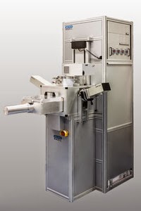
Colnatec is expanding its portfolio of high-precision, thin film measurement and control devices, Colnatec today announced the debut of a compact controller that unites the leading-edge technology of its Eon™ series of PC-based controllers with the modular efficiency of rackmount instrumentation.


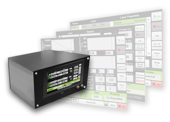
Thin Film Controller with Integrated Display
Adaptable. Affordable. Unconventional.


With its integrated display, intuitive user interface, and durable architecture, Eon-ID™ offers a versatile design that adapts easily to a variety of settings - ranging from industrial to laboratory to clean room to research environments - matching or surpassing the capabilities of Inficon™ XTC/3™ and IC6™.

“We’ve identified a growing demand for a stand-alone thin film control solution that incorporates hardware, display, and software into a single enclosure,” said Colnatec CTO Scott Grimshaw. “In answering this demand, Eon-ID™ has exceeded our expectations. Making thin film control more accessible through affordability and efficiency of design, Eon-ID™ has the potential of not only broadening thin film science in general but driving thin film manufacturing opportunities into completely new and unexpected areas of industry.”

Among its numerous features, Eon-ID™ offers the latest Eon Software™ interface, an integrated display allowing for a greater variety of settings and applications, rackmount capability, a temperature compensation system that maintains crystal to within +/- 1°C of preset temperatures, advanced technology that increases reliability and durability in industrial environments.

"Eon-ID™ employs the same temperature-centric technology used in our Eon™ and Eon-LT™ series controllers," noted Colnatec CEO Wendy Jameson. "Eon-ID™ will specifically benefit industries using atomic layer deposition (ALD), optics, OLED, and any other process that requires precision control over very thin layers, especially at temperatures higher than 100°C. Combining precision, simplicity, and cost effectiveness, Eon-ID™ represents nothing less than the state-of-the-art in thin film science."

About Colnatec

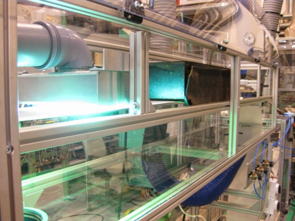
Taking a revolutionary approach to thin film design, development, and manufacturing, Colnatec (colnatec.com) manufactures the only commercially available heated quartz crystal microbalances (QCM) for process control of film thickness measurement in high temperature processes such as atomic layer deposition (ALD) or chemical vapor deposition (CVD). Through the use of patented and patent-pending Colnatec technology, researchers, manufacturers, and system-builders have reduced production and run times and costs to improve overall performance - ultimately achieving higher yields and improved process control. Colnatec technology is also frequently used in, encapsulation and high flux deposition of organic light emitting diodes (OLED), optical coatings such as for anti-reflection (PVD), next generation food packaging, and medical device coating, etc. Launched in 2009, Colnatec is the recipient of Department of Energy Phase I and Phase II SBIR awards for high temperature sensors, and one of eight winners of the inaugural Arizona Commerce Authority Innovation Challenge Grant. Colnatec has built a reputation as a bold innovator and a formidable player in a tough, highly competitive marketplace.

Sunday, November 9, 2014

Polymer hybrid thin-film composites for food packaging and membrane filters

As reported by VTT: Juha Nikkola M.Sc.(Tech.), Senior Scientist at VTT Technical Research Centre of Finland, developed new hybrid materials in his doctoral research project for use in the manufacture and modification of thin-film composites. The project resulted in new materials suitable for instance for food packaging with enhanced diffusion barrier and for membrane filters with improved anti-fouling properties used in water purification. In the future, similar materials may find use in flexible OLED displays and in wall and ceiling panels.

The doctoral research project involved developing surface materials that decrease bacterial adhesion to the surface. Improved surface materials can help keep membrane filters or wall surfaces clean or improve the preservation of food.

Food spoilage can be delayed with a new type of cardboard package coated with a plastic incorporating the thin-film composite structure developed in the present project. Such diffusion barrier materials may also find use in flexible OLED displays in the electronics industry or in replacing thickly layered paint on wall and ceiling panels.

The doctoral research project involved studying and developing flexible thin-film composites using various coating techniques and studying the impact of the surface layer on the permeability and anti-fouling properties of the thin-film composite. The hybrid materials developed can be produced in roll-to-roll processing. The research focused on atmospheric plasma deposition, atomic layer deposition (ALD) and sol-gel deposition techniques.


Thin-film composites can be manufactured using a roll-to-roll process. The photo shows the VTT coating production line.

A hybrid material is simply a combination of two materials at the macro, micro or nano level. Hybrid material is typically a blend, multilayer or nanostructured material. For instance, multilayer structures manufactured using thin-film deposition techniques can be named as hybrid materials.

Thin-film composites usually consist of three layers with different functions. The support and core layers provide the mechanical properties such as strength and flexibility. The core layer may also have properties affecting the chemical durability, permeability or composition of the composite. The properties required of the skin layer may have to do with separation efficiency, diffusion barrier performance, roughness, surface energy or liquid or gas permeability.

Juha Nikkola will defend his doctoral dissertation at the Tampere University of Technology on 31 October 2014 at 12.00.

The thesis is available online at Polymer hybrid thin-film composites with tailored permeability and anti-fouling performance: http://www.vtt.fi/inf/pdf/science/2014/S66.pdf


Conformal organohalide perovskite laser by realized ALD


As reported by Nanotechweb : Researchers at the University of Toronto in Canada say that they have made the first perovskite-based spherical resonator laser by coating organometallic halide perovskites uniformly onto glass microspheres. The device might be employed in novel optical communications applications, and the new structure also shows promise for solar cells and photodetectors.

Obviously it has been done by ALD!

The Toronto team, led by Edward Sargent, employed an industry-standard technique, known as atomic layer deposition (ALD), to grow high-quality one-atom seed layers of lead sulphide and then developed a way to “exchange” these PbS layers with perovskite by exposing them to iodine gas vapour and methylammonium iodide. The resulting structure – a highly pure, polycrystalline film of CH3NH3PbI3 perovskite – can then be coated onto a spherical optical cavity made from a glass microsphere (see figure). This optical cavity lases when pumped with green, red or blue light.

Check out the full story here and the paper below.

Brandon R. Sutherland , Sjoerd Hoogland, Michael M. Adachi, Chris T. O. Wong, and Edward H. Sargent
ACS Nano, 2014, 8 (10), pp 10947–10952


Conformal integration of semiconductor gain media is broadly important in on-chip optical communication technology. Here we deploy atomic layer deposition to create conformally deposited organohalide perovskites—an attractive semiconducting gain medium—with the goal of achieving coherent light emission on spherical optical cavities. We demonstrate the high quality of perovskite gain media fabricated with this method, achieving optical gain in the nanosecond pulse regime with a threshold for amplified spontaneous emission of 65 ± 8 μJ cm–2. Through variable stripe length measurements, we report a net modal gain of 125 ± 22 cm–1 and a gain bandwidth of 50 ± 14 meV. Leveraging the high quality of the gain medium, we conformally coat silica microspheres with perovskite to form whispering gallery mode optical cavities and achieve lasing

Saturday, November 8, 2014

NCSU show conductive Kevlar by Tungsten ALD coating

As reported by Laboratory Equipment: A group of North Carolina State Univ. researchers is exploring novel ways to apply semiconductor industry processes to unique substrates, such as textiles and fabrics, to "weave together" multifunctional materials with distinct capabilities.

During the AVS 61st International Symposium & Exhibition, being held November 9-14, 2014, in Baltimore, Maryland, the researchers will describe how they were able to weave high-strength, highly conductive yarns made of tungsten metal on Kevlar — body armor material — by using atomic layer deposition (ALD), a process commonly used for producing memory and logic devices.


Tungsten-coated Kevlar with a Kevlar (uncoated) background. Image: S. Atanasov, NCSU

The group's tungsten-on-Kevlar yarns are expected to find applications in multifunctional protective electronics materials for electromagnetic shielding and communications, as well as erosion-resistant antistatic fabrics for space and automated technologies


Stabilization of ALD barrier film by MLD interlayers by TU Dresden


Christoph Hossbach, Frederik Nehm, Aarti Singh, Hannes Klumbies, Dustin Fischer, Claudia Richter, Uwe Schroeder, Matthias Albert, Lars Müller-Meskamp, Karl Leo, Thomas Mikolajick and Johann W. Bartha

J. Vac. Sci. Technol. A 33, 01A119 (2015); http://dx.doi.org/10.1116/1.4901232

Diffusion barrier stacks for the encapsulation of organic electronics made from inorganic nanolaminates of Al 2O3 and TiO2 with aluminum alkoxide interlayers have been deposited byatomic layer deposition (ALD) and molecular layer deposition (MLD). As a part of the MLD process development, the deposition of aluminum alkoxide with low a density of about 1.7 g/cm3was verified. The ALD/MLD diffusion barrier stack is meant to be deposited either on a polymer film, creating a flexible barrier substrate, or on top of a device on glass, creating a thin-filmencapsulation. In order to measure the water vapor transmission rate (WVTR) through the barrier, the device is replaced by a calcium layer acting as a water sensor in an electricalcalcium test. For the barrier stack applied as thin-film encapsulation on glass substrates, high resolution scanning electron microscopy investigations indicate that the inorganic nanolaminates without MLD interlayers are brittle as they crack easily upon the stress induced by the corroding calcium below. The introduction of up to three MLD interlayers of 12 nm each into the 48 nm barrier film laminate successfully mitigates stress issues and prevents the barrier from cracking. Using the three MLD interlayer configurations on glass, WVTRs of as low as 10−5g/m2/d are measured at 38 °C and 32% relative humidity. On polymer barrier substrates, thecalcium is evaporated onto the barrier stack and encapsulated with a cavity glass. In this configuration, the corroding calcium has space for expansion and gas release without affecting the underlying barrier film. In consequence, a WVTR of about 3 × 10⁻³ g/m2/d is measured for all samples independently of the number of MLD interlayers. In conclusion, a stabilization and preservation of the ALD barrier film against mechanical stress is achieved by the introduction of MLD interlayers into the inorganic nanolaminate.


Schematic drawing of a Ca test built on an ALD barrier coated foil substrate (barrier film test configuration)


Top view of glass Ca tests coated with ALD/MLD barrier stacks consisting of a 48 nm Al-O/Ti-O nanolaminate with zero to three aluminum alkoxide interlayers of 12 nm thickness. The layers were deposited at 90 °C on Ca tests on glass and aged at 38 °C and 32% r.h.—picture taken with high resolution scanning electron microscopy after aging.


Wednesday, November 5, 2014

ALD of L-Alanine Polypeptide by Sandia, University of New Mexico and Angstrom Thin Film Tech

 
Yaqin Fu, Binsong Li, Ying-Bing Jiang, Darren R. Dunphy, Andy Tsai, Siu-Yue Tam, Hongyou Fan, Hongxia Zhang, David Rogers, Susan Rempe, Plamen Atanassov, Joseph L. Cecchi, and C. Jeffrey Brinker
J. Am. Chem. Soc., Article ASAP, DOI: 10.1021/ja5043403, Publication Date (Web): October 30, 2014


l-Alanine polypeptide thin films were synthesized via atomic layer deposition (ALD). Instead of using an amino acid monomer as the precursor, an l-alanine amino acid derivatized with a protecting group was used to prevent self-polymerization, increase the vapor pressure, and allow linear cycle-by-cycle growth emblematic of ALD. The successful deposition of a conformal polypeptide film has been confirmed by FTIR, TEM, and Mass Spectrometry, and the ALD process has been extended to polyvaline.

Call for Abstracts - ALD 2015: June 28-July 1, Portland, Oregon

Call for Abstracts - ALD 2015: June 28-July 1, Portland, Oregon
 
Abstract Deadline: February 16, 2015
The conference will cover a wide range of topics including the following. Prospective authors are invited to Submit Online
 
ALD FUNDAMENTALS:

Precursors and Chemistry
  • Precursor Design, New Precursors, Recipe Development
  • Simulation, Modeling, and Theory of ALD
  • Precursor Delivery Systems
Growth and Characterization
  • In-situ Monitoring and Analysis
  • ALD Surface Chemistry and Initiation of Growth
  • Surface Preparation for ALD
  • Characterization of ALD Coatings
  • Highly Conformal ALD Processes
  • Plasma Enhanced ALD Processes
  • Electrochemical (EC) ALD Processes
Novel Materials
  • Molecular Layer Deposition
  • Organic-Inorganic Hybrid Materials
  • Atomic Layer Epitaxy and Doping
  • Magnetic Materials
  • ALD Coating of Powder
NANOSTRUCTURE SYNTHESIS AND FABRICATION:
  • Selective ALD Growth, Patterning
  • Nanotubes, Nanowires, Nanopores
  • Nanoparticles
  • Nanolaminates 2D Nanomaterials (Including Transition Metal Dichalcogenides)
ALD APPLICATIONS:
  • Energy
  • Catalysis and Fuel Cells
  • Solar Energy Materials
  • Batteries and Energy Storage
Applications in ULSI FEOL and BEOL
  • High-k Applications
  • Gate Electrode
  • Contact Metal
  • 3D Transistor Fabrication
  • Interconnects
  • Cu Diffusion Barriers
  • Cu Capping Technologies
  • Low-k Pore Sealing
  • Low-k Spacer
Memory Applications
  • DRAM
  • Flash Memory
  • MRAM
  • RRAM
  • Other Non-volatile Memories
ALD FOR MANUFACTURING
  • Reactor and Equipment Design for Manufacturing
  • ALD Reactor Modeling
  • Large Format ALD
  • Spatially Controlled ALD
  • Sensing and Process Control
  • Fast ALD
  • R2R