Wednesday, November 5, 2014

Call for Abstracts - ALD 2015: June 28-July 1, Portland, Oregon

Call for Abstracts - ALD 2015: June 28-July 1, Portland, Oregon
 
Abstract Deadline: February 16, 2015
The conference will cover a wide range of topics including the following. Prospective authors are invited to Submit Online
 
ALD FUNDAMENTALS:

Precursors and Chemistry
  • Precursor Design, New Precursors, Recipe Development
  • Simulation, Modeling, and Theory of ALD
  • Precursor Delivery Systems
Growth and Characterization
  • In-situ Monitoring and Analysis
  • ALD Surface Chemistry and Initiation of Growth
  • Surface Preparation for ALD
  • Characterization of ALD Coatings
  • Highly Conformal ALD Processes
  • Plasma Enhanced ALD Processes
  • Electrochemical (EC) ALD Processes
Novel Materials
  • Molecular Layer Deposition
  • Organic-Inorganic Hybrid Materials
  • Atomic Layer Epitaxy and Doping
  • Magnetic Materials
  • ALD Coating of Powder
NANOSTRUCTURE SYNTHESIS AND FABRICATION:
  • Selective ALD Growth, Patterning
  • Nanotubes, Nanowires, Nanopores
  • Nanoparticles
  • Nanolaminates 2D Nanomaterials (Including Transition Metal Dichalcogenides)
ALD APPLICATIONS:
  • Energy
  • Catalysis and Fuel Cells
  • Solar Energy Materials
  • Batteries and Energy Storage
Applications in ULSI FEOL and BEOL
  • High-k Applications
  • Gate Electrode
  • Contact Metal
  • 3D Transistor Fabrication
  • Interconnects
  • Cu Diffusion Barriers
  • Cu Capping Technologies
  • Low-k Pore Sealing
  • Low-k Spacer
Memory Applications
  • DRAM
  • Flash Memory
  • MRAM
  • RRAM
  • Other Non-volatile Memories
ALD FOR MANUFACTURING
  • Reactor and Equipment Design for Manufacturing
  • ALD Reactor Modeling
  • Large Format ALD
  • Spatially Controlled ALD
  • Sensing and Process Control
  • Fast ALD
  • R2R

Thursday, October 30, 2014

Toyota funds ALD technology research for battery materials at Aalto University, Finland

"Toyota enthusiastic over Aalto’s materials research" Professor Maarit Karppinen’s research group is developing better battery materials by means of atomic layer deposition.
 

The car-manufacturing giant found Aalto University and Maarit Karppinen’s research group on the basis of a recommendation.‘They bought the reactor needed for atomic layer deposition from Picosun, a Finnish company that told them we would have the research expertise they needed,’ explains doctoral researcher Mikko Nisula, who works in Professor Karppinen’s group.

‘It’s great that an international car-manufacturing giant is capable in practice of utilizing the long-term basic research with ALD technology we’ve been doing. The cooperation has advanced quite smoothly,’ Professor Karppinen says.


More information:
Doctoral candidate Mikko Nisula, Aalto University School of Chemical Technology, Department of Chemistry
mikko.nisula@aalto.fi

Professor Maarit Karppinen, Aalto University School of Chemical Technology, Department of Chemistry
maarit.karppinen@aalto.fi

Wednesday, October 29, 2014

Ferroelectricity in Si-doped HfO2 Revealed: A Binary Lead-free Ferroelectricby ALD

Scientists at Namlab gGmbH, Leibniz Institute for Solid State and Materials Research and Fraunhofer IPMS-CNT Dresden, Germany together with Center for Nanophase Materials Sciences, Oak Ridge National Laboratory, TN, USA provides conclusive evidence to intrinsic ferroic behavior in Si-doped HfO2.

 Dominik Martin, Johannes Müller, Tony Schenk, Tomas M. Arruda, Amit Kumar, Evgheni Strelcov, Ekaterina Yurchuk, Stefan Müller, Darius Pohl, Uwe Schröder, Sergei V. Kalinin, and Thomas Mikolajick

Advanced Materials Article first published online: 28 OCT 2014

Static domain structures and polarization dynamics of silicon doped HfO2 are explored. The evolution of ferroelectricity as a function of Si-doping level driving the transition from paraelectricity via ferroelectricity to antiferroelectricity is investigated. Ferroelectric and antiferroelectric properties can be observed locally on the pristine, poled and electroded surfaces, providing conclusive evidence to intrinsic ferroic behavior.


One ALD layer can increase the efficiency of photoelectrodes for water splitting

Here is a new paper from Massimo Tallarida and co-workers group in Cottbus at Brandenburg University of Technology in collaboration with Helsinki, Tartu and Alicante. The published paper below in Journal of Physical Chemistry Letters, gives for the first time a reasonable explanation of why 1 ALD layer can increase the efficiency of photoelectrodes for water splitting, just using the chemistry of ALD (in particular, only TMA).


Modification of Hematite Electronic Properties with Trimethyl Aluminum to Enhance the Efficiency of Photoelectrodes

Massimo Tallarida, Chittaranjan Das, Dejan Cibrev, Kaupo Kukli, Aile Tamm, Mikko Ritala, Teresa Lana-Villarreal, Roberto Gómez, Markku Leskelä, and Dieter Schmeisser

J. Phys. Chem. Lett., 2014, 5 (20), pp 3582–3587
 
 
The electronic properties of hematite were investigated by means of synchrotron radiation photoemission (SR-PES) and X-ray absorption spectroscopy (XAS). Hematite samples were exposed to trimethyl aluminum (TMA) pulses, a widely used Al-precursor for the atomic layer deposition (ALD) of Al2O3. SR-PES and XAS showed that the electronic properties of hematite were modified by the interaction with TMA. In particular, the hybridization of O 2p states with Fe 3d and Fe 4s4p changed upon TMA pulses due to electron inclusion as polarons. The change of hybridization correlates with an enhancement of the photocurrent density due to water oxidation for the hematite electrodes. Such an enhancement has been associated with an improvement in charge carrier transport. Our findings open new perspectives for the understanding and utilization of electrode modifications by very thin ALD films and show that the interactions between metal precursors and substrates seem to be important factors in defining their electronic and photoelectrocatalytic properties.
 
 
The building Panta Rhei, home for the Chair of Applied Physics and Sensors (Prof. Dr. Dieter Schmeißer) at Brandenburg Universitxy of Technology. The main research area of the department is spectroscopic and micro spectroscopic investigation of layers and layer structures in order to get information about the electronic properties and the geometrical structures of several materials, such as high-k oxides, metal and mixed oxides, inter metallic interfaces, semiconductors, conducting and semiconducting polymers, and with recent focus graphene. In addition, the department is very active in the research area of atomic layer deposition (ALD). In particular the initial layer growth is in the focus of interest. The layer deposition as well as the characterization are done in situ = "(in situ)2", where the characterization can be performed "cycle by cycle". (further information)

The authors conclude that the ALD of Al2O3 based on TMA produces modifications in the electronic properties of α-Fe2O3 favoring the improvement of its photoelectrochemical behavior. Reactions between TMA and α-Fe2O3 induce electron donation to the substrate in the form of small polarons and modify the covalent character of the Fe−O bonds. These Fe2O3 surface modifications probably allow for an enhanced charge carrier transport next to the interface and explain the photoelectrochemical enhancement observed in hematite photoanodes. We believe that this work contributes to the understanding of some of the mechanisms underlying the enhancement of hematite photoanodes by means of surface modification and that it may open new avenues for further improving their performance in the context of water splitting.


A vision of a sustainable hydrogen fuel community based on Artificial photosynthesis (APS) has been described in man yplaces and in particular in a relatively recent review in Nature Photonics (here).


Vision of a sustainable hydrogen fuel community based on Artificial photosynthesis (APS) - Hydrogen is produced from an APS solar water-splitting power plant using seawater on floating ports, tankers and seashore plants. Electricity needed to operate such an infrastructure is provided by renewable energy sources such as photovoltaic, wind and tidal power. (Nature Photonics, 6 (2012) 511)


Friday, October 17, 2014

A Short History of Atomic Layer Deposition: Tuomo Suntola's Atomic Layer Epitaxy

 
Chem. Vap. Dep. Article first published online: 15 OCT 2014
DOI: 10.1002/cvde.201402012

Atomic layer deposition (ALD) is a thin film growth technique based on the repeated use of separate, saturating gas-solid reactions. The principle of ALD has been discovered twice; in the 1960s under the name “molecular layering” in the Soviet Union, and in the 1970s under the name “atomic layer epitaxy” (ALE) in Finland. In 2014, it is forty years since the filing of the worldwide patent on ALE as a method for the growth of compound thin films. This essay celebrates the fortieth anniversary of ALE-ALD, briefly telling the story of ALE as shared by its Finnish inventor, Dr. Tuomo Suntola. Initially, ALE was aimed at the growth of high-quality polycrystalline ZnS thin films for electroluminescent (EL) display panels. Gradually, the material selection of ALE increased, and the application areas were extended to photovoltaics, catalysis, semiconductor devices, and beyond. Fast, production-worthy ALE reactors were imperative for industrial success. The unprejudiced creation of new technologies and products with ALE, initiated by Dr. Tuomo Suntola and led by him until early 1998, are an integral part of the Finnish industrial history, the fruits of which are seen today in numerous applications worldwide.
 

Sven Lindfors in 1978 next to the flow-type ALD reactor in which the successful H2S/ZnCl2 process was demonstrated.


* The author thanks Tuomo Suntola for sharing these and other details of the development of ALE and EL. It has been a great honor and privilege to work with him and to write this history. Writing this history was triggered by the parallel-running worldwide Virtual Project on the History of ALD (VPHA). Warmest thanks to Tuomo Suntola for his support for the VPHA, too. The author also acknowledges Tapio Alvesalo for checking the details related to NAPS, Dr. Marko Tuominen for the details related to ASM Microchemistry, Juhana Kostamo for the details related to Picosun, Prof. Victor Drozd for confirming the timing of Suntola's visit to Leningrad, Prof. Yukihiro Shimogaki and Prof. Markku Leskelä for identifying the second-left participant in the ALE-1 photograph, and Prof. David Cameron for polishing the language in this article. Funding by the Academy of Finland's Centre of Excellence in Atomic Layer Deposition (ALDCoE) is gratefully acknowledged.

Thursday, October 16, 2014

3 min pitch - Protective coatings for silver cultural heritage objects using ALD

Novel protective coatings for silver alloy cultural heritage objects using atomic layer deposited metal oxide barrier films. This is one of the video pitches from the 17 PhD students from around the world who have made it to the final of a competition that challenges them to present their research in only three minutes.


2014 U21 3MT® Finalist - Amy Elizabeth Marquardt. Amy is a finalist in the U21 Three Minute Thesis (3MT) Competition. If you like her presentation, please vote for it here: http://www.u213mt.com/index.php. Voting ends October 20th.

Tuesday, October 14, 2014

Levitech 5 Year Anniversary - ALD4INDUSTRY Workshop

Levitech will celebrate its 5th Anniversary on Thursday October  30th, 2014 with a Workshop Program and an Anniversary Program  at Levitech in Almere. "For this day Levitech invited several national and international  speakers from the field of Atomic Layer Deposition. The topics of  these workshops are ‘ALD4IC’, ‘ALD4PV’ and ‘Innovation4PV’.  During the lunch buffet and dinner you have the opportunity to  network. Please join us on this day."


PROGRAM ALD4INDUSTRY
Thursday October 30, 2014 Levitech BV, Almere, The Netherlands

09.30 Welcome Workshop Program
09.55 Opening by Jaap Beijersbergen

Presentations ALD4IC

10.00 Suvi Haukka (ASM)
10.45 Sven van Elshocht (IMEC)

Presentation Innovation4Industry

11.15 Markus Fischer (Hanwha Q-Cells)
12.15 Lunch buffet

Presentations ALD4PV

13.15 Erwin Kessels (TUE)
14.00 Ilkay Cesar (ECN)
14.30 Willem Jan Huisman (ASM)
15.00 Ernst Granneman (Levitech)

15.30 Welcome Anniversary Program

Presentations

16.00 Wim Sinke (ECN)
16.45 Jan Nico Appelman (Flevoland)
17.00 Levitech 5 Years Anniversary
17.30 Dinner


Saturday, October 11, 2014

Nanjing Tech University demonstartes paper-based membranes for oil/water separation by ALD

Nanjing Tech University demonstartes low-cost but highly efficient paper-based membranes for oil/water separation through hydrophobic modification to filter papers by ALD.
 
Liang Kong, Qianqian Wang, Sen Xiong, and Yong Wang
Ind. Eng. Chem. Res., September 30, 2014


It remains a great challenge for the simple and affordable production of membranes for oil/water separation. We prepare low-cost but highly efficient paper-based membranes for oil/water separation through hydrophobic modification to filter papers. The simple modification contains only two steps: a thin layer of aluminum oxide is first coated on the surface of the filter paper by atomic layer deposition, and silane molecules are subsequently coupled on the precoated aluminum oxide layer via their reaction with hydroxyl groups on the surface. Both the alumina layer and the silanization layer are very thin with a total thickness less than 10 nm. The modified filter paper is endowed with strong hydrophobicity and oleophilicity, therefore exhibits strongly retarded permeation to water and enhanced permeation to nonpolar oils. The modified filter paper is demonstrated to show excellent separation efficiencies greater than 90% in the separation of various types of oils and organic solvents from their mixtures with water. The paper-based membranes prepared in this work are distinguished among others for their low-cost substrates and simple modification route. This modification method is expected to be easily extended to hydrophobize a diversity of other substrates.

Wednesday, October 8, 2014

Voilà - 3rd ALD Lab Dresden Symposium at SEMICON Europa was a success!

For the 3rd time ALD Lab Dresden organised The ALD Lab Dresden Symposium at SEMICON Europa - this time in Grenoble, France. Our workshop, wants to stimulate discussions between developers of tools, consumables, as well as applicants of this exciting technology. Here are some pictures from the event.


Prof. Johan W. Bartha, Institut für Halbleiter- und Mikrosystemtechnik, TU Dresden, Germany introduces ALD Lab Dresden to the audiance and opens the Symposium with a talk on “Fundamental insight into ALD processing by in-situ observation”
 

Malte Czernohorsky, Fraunhofer IPMS-CNT, Dresden, Germany presenting results from the EU PICS Project "Development of innovative ALD materials and tools for high density 3D integrated capacitors"
 
 
Mickael Gros-Jean, ST Microelectronics, Grenoble, France giving a talk on "High permittivity dielectrics for CMOS FDSOI Gate first technologiess"
 
 
Stefan E. Schulz, Fraunhofer ENAS, Chenitz, Germany getting ready to give his talk on "ALD of Metals and Metal Oxides for Advanced Interconnect and Sensor Technology: In-Situ Investigations for the ALD of Copper"


Beneq expands local US service capabilities through Maxima Sciences

Beneq Thin Film Equipment has entered an agreement with Maxima Sciences of Cincinnati, Ohio, to offer maintenance and service closer to its customers located throughout North America. This collaboration will enable faster response times and local support for Beneq’s atomic layer deposition (ALD) customers.
 

Now, in addition to an existing service hub at the main office in Finland that supports European customers, and a service hub in Shanghai, China, serving customers throughout Asia, this agreement with Maxima Sciences fills the gap in service provision for the North American region. The service network expansion will enable Beneq to provide better and faster local support for more of its ALD customers when it comes to questions they may have with their processes or equipment.

Beneq’s services include spare parts, process and/or equipment upgrades, along with regular and periodic maintenance calls and audits. Additionally, Beneq’s coating service and application development capabilities can now be provided locally through Maxima Sciences.

Maxima Sciences is a custom scientific instrument design and fabrication specialist. Like Beneq, the company has ALD as one of its primary areas of expertise. Among the other services offered by Maxima Sciences are instrument design, precision machining, vacuum chambers and components, electronics, glass blowing and repairs.

“We’re excited about working closely with Beneq and taking advantage of the company’s strong ALD technology know-how. Both companies have considerable experience with ALD. With this agreement, we’re looking forward to teaming up with the world leader in this field,” says Dr Jacob Bertrand, President, Maxima Sciences.

The principal point of contact for service calls at Beneq is service(at)beneq.com. See our homepage for more information.

Sunday, October 5, 2014

Scandinavian Nanotechnology Market Reports from AZO Nano

AZO Nano has published Market Reposrts on Scandinavian Nanotechnology (Norway is missing) The reports are available online and include the following :

  • A brief introduction to the key nanotechnology-related organizations
  • The major nanotechnology-related companies are listed below along with a brief introduction to each of them.
  • The leading academic institutes in that are offering courses and research programs in nanoscience and nanotechnology are listed

Direct links to the reports:

Nanotechnology in Sweden: Market Report
Nanotechnology in Finland: Market Report
Nanotechnology in Denmark: Market Report

Saturday, October 4, 2014

The Stanford Nanofabrication Facility Labmembers Wiki

The Stanford Nanofabrication Facility has a SNF Labmembers Wiki open to read for everyone describing all equipment and processes they are operating - impressive! : "This wiki site is for and by the SNF lab community. It's a resource for working inside the lab, serving as a dynamic reference as well as historical archive. For more general topics about SNF (such programs in education, how to join, directions, history) please see the Stanford Nanofabrication Facility Home Page.  A login is not needed to view public information, only to contribute.  If you are a labmember wishing to contribute, contact an SNF staff member for access."
 
 
Some useful ALD information that I found while surfing around among other equipment for nanofabrication : 
 
 
Detailed information on ALD tools and processes operated by SNF:
  • Savannah S200 from Cambridge Nanotech/Ultratech
  • A system called MVD that is a system consisting of a glovebox, plasma cleaner, and Savannah ALD tool which is used to deposit organic SAMS layers
  • 3(!) Fiji ALD system from Cambridge Nanotech/Ultratech dedictaed for different processes
ALD introductory tutorial and In-depth tutorial presented by Dr. J Provine 11/1/12 at Stanford University
 
 
A system called MVD that is a system consisting of a glovebox, plasma cleaner, and Savannah ALD tool which is used to deposit organic SAMS layers (picture from SNF wiki)


Tour of the Stanford Nanofabrication Facility we look at some of the key steps and equipment involved in nanofabrication. at 09:45 the introduce ALD and a Fiji reactor and starting a run on a Savannah. (Youtube).

Friday, October 3, 2014

ALD of LiFePO4 as a High-Performance Cathode for Lithium-Ion Batteries

Dr. Sun’s Nanomaterials & Energy Group at University of Western Ontario just published a very interesting paper on lithium iron phosphate by ALD for 3D solid state microbatteries in Advanced Materials. 
 

Western Engineering professor Andy Sun, Canada Research Chair in Development of Nanomaterials for Clean Energy, is working toward increasing the performance of electric cars, by using lithium iron phosphate batteries (Professor charges toward better battery life).
 

Jian Liu, Mohammad N. Banis, Qian Sun, Andrew Lushington, Ruying Li, Tsun-Kong Sham, and Xueliang Sun
Adv. Mater. 2014, 26, 6472–6477
 
The atomic layer deposition technique is successfully applied to synthesize lithium iron phosphate using rationally designed surface reactions, as demonstrated for the first time by X. Sun and co-workers on page 6472. The lithium iron phosphate exhibits high power density, excellent rate capability, and ultra-long lifetime, showing great potential in vehicular lithium batteries and 3D all-solid-state microbatteries.

Herein, for the fi rst time, we develop an ALD approach to grow LiFePO 4*, as a typical example of quaternary LiMPO 4 cathode materials, by carefully tailoring the surface reactions that occur. Distinguished from solid-state reactions and solution chemistries, the ALD approach employs self-limiting, vapor-based surface reactions to deposit LiFePO 4 in a layer-bylayer manner (Fe 2 O 3 , PO x , and Li 2 O subcycles). In this way, the ALD approach permits precise control over the thickness and film composition of LiFePO 4 at the atomic level. This unprecedented accuracy promises a versatile design of nanostructured LiFePO4 on various types of substrates (in particular with high aspect ratio), and extends the employment of LiFePO4 to a broader range of applications, especially in 3D all-solid state microbatteries for autonomous micro-devices. Moreover, LiFePO 4 is deposited on carbon nanotubes (CNTs) by ALD to form LiFePO4 /CNT nanocomposite, aiming at breaking through the rate-capability bottleneck typically for pristine LiFePO4 . Excitingly, the LiFePO 4 /CNT electrode exhibits excellent rate capability, high power density, and ultra-long cycling lifetime, which are desirable properties for vehicular LIBs. Our work provides a new method for well-defined fabrication of high-powered.

* Amorphous LiFePO 4 at 300 °C with the use of ferrocene (FeCp2), ozone (O3), trimethylphosphate (TMPO), water (H2O), and lithium t -butoxide (LiOtBu) as precursors.
 
 
Here is an earlier review form 2012 :
 
Emerging Applications of Atomic Layer Dposition for Lithium-ion Battery Studies

X. Meng, X.-Q. Yang, X. Sun
Adv. Mater. 24 (2012) 3589-3615.
 
Lithium-ion batteries (LIBs) are used widely in today's consumer electronics and offer great potential for hybrid electric vehicles (HEVs), plug-in HEVs, pure EVs, and also in smart grids as future energy-storage devices. However, many challenges must be addressed before these future applications of LIBs are realized, such as the energy and power density of LIBs, their cycle and calendar life, safety characteristics, and costs. Recently, a technique called atomic layer deposition (ALD) attracted great interest as a novel tool and approach for resolving these issues. In this article, recent advances in using ALD for LIB studies are thoroughly reviewed, covering two technical routes: 1) ALD for designing and synthesizing new LIB components, i.e., anodes, cathodes, and solid electrolytes, and; 2) ALD used in modifying electrode properties via surface coating. This review will hopefully stimulate more extensive and insightful studies on using ALD for developing high-performance LIBs.


Tuesday, September 30, 2014

High-k für Alle - High-k/Metal Gates in the 2010s by Dick James Chipworks

High-k für Alle - A very nice overview of the High-k/Metal Gate transistors that enabled the mobile revolution that we have enjoyed in the last years. Atomic Layer Deposition is definitely part of this revolution amongst other semiconductor manufacturing techniques. Originally published for the Advanced Semiconductor Manufacturing Conference (ASMC), 2014 25th Annual SEMI (19-21 May 2014) by Dick James at Chipworks. Many of these has been published earlier by Chipworks and this paper covers them all and is therefore a very good overview for anyone into high-k and modern transistors.
 
 
Dick James Chipworks Inc., Ottawa, ON, Canada
 
 
Dick James Chipworks Inc., Ottawa, ON, Canada
Advanced Semiconductor Manufacturing Conference (ASMC), 2014 25th Annual SEMI, DOI: 10.1109/ASMC.2014.6846970
Abstract: 2007 saw the introduction of the first high-k/metal gate (HKMG) devices into the marketplace. This marked the return of metal-gate technology on silicon for the first time since polysilicon gates became ubiquitous in the early 1970s. Intel was the first to use high-k/metal gate in its 45-nm product. Other leading-edge manufacturers have now launched HKMG products in both gate-first and gate-last forms at the 28-nm node, and we have seen the first HKMG finFET products from Intel. In the near future we also expect to see the first 20-nm foundry products come onto the market. Chipworks, as a supplier of competitive intelligence to the semiconductor and electronics industries, monitors the evolution of chip processes as they come into commercial production. Chipworks has obtained parts from the leading edge manufacturers, and performed structural analyses to examine the features and manufacturing processes of the devices. The paper discusses some of the different transistor structures we have seen during the evolution of the HKMG technology, and examines the variety of 32/28-nm parts that have been introduced. We will also show more details of the Intel 22-nm finFETs.
 
The paper covers eight of the transistor structures that have made it into production in the last two years. HKMG processes in the industry have bifurcated into gate-first (IBM, GLOBALFOUNDRIES, Samsung) and gate-last (Intel, TSMC), with different implementations within each group. At the 20-nm node the majority of processes will migrate to planar gate-last, with IBM staying with the gate-first technology for their in-house products. Below 20-nm, we will start to see other finFET processes come into production
 
32/28 nm Transistors
  • Qualcomm Snapdragon 800 (TSMC 28HPM)
  • Rockchip RK3188 (GLOBALFOUNDRIES 28SLP)
  • Apple/Samsung A5 APL2498 (Samsung HKMG 32LP)
  • Apple/Samsung A7 APL0698 (Samsung HKMG 28LP)
  • IBM Power 7+ (IBM HKMG 32HP SOI)
  • Texas Instruments OMAP5432 (UMC Poly/SiON 28LP)


TSMC 28HPM PMOS transistor (Chipworks)
 
22 nm Transistors
  • Intel E-1230 Xeon
  • Intel Atom “Baytrail” SoC

Intel 22nm SoC transistor options (Chipworks)


The National Science Foundation Funds Three Penn State Teams to Study Two-Dimensional Materials

 As reported by Newswise — Through the National Science Foundation’s Emerging Frontiers in Research and Innovation (EFRI) program, Penn State has been awarded $4 million over the next four years to lead two teams of investigators and support members of a third team in the new field of 2D crystals and layered materials.

A material that is only a single atomic-layer thick can have completely different properties than its bulk counterpart. A new field of nanoscale science and engineering is emerging to study the wide variety of two-dimensional materials and what happens when they are stacked one on top of the other. Potential applications include energy harvesting and storage, sensing, electronics and photonics, and bioengineering.

“There is a lot of interest in 2D materials beyond graphene, especially when considering stacking to form heterostructures because they can lead to phenomenal properties,” said Joshua Robinson, Corning Faculty Fellow of Materials Science and Engineering and associate director of Penn State’s Center for Two-dimensional and Layered Materials (2DLM). “I think we have a variety of excellent ideas in these novel materials, which is why we did so well with the EFRI.”
 
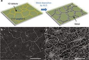
Crystalline large area WS2 have been grown directly on SiO2/Si substrates. The top left panel exhibits a high resolution transmission electron microscopy (HRTEM) image of the edge of a single-layer WS2 film. The top left panel depicts a schematic representation of the as grown WS2 film. A photograph of a WS2 film transferred onto a substrate is shown on the right panel, exhibiting the high contrast of the WS2 over SiO2/Si (films are cyan in color). (Picture from Ana Laura Elias, Penn State, Newswise)

The EFRI awards fund interdisciplinary teams of researchers in rapidly advancing fields of fundamental engineering research. The 2014 awards, called 2-DARE, for Two-dimensional Atomic-layer Research and Engineering, were awarded to nine teams in the U.S., three of which include Penn State researchers.

• “2D Crystal Formed by Activated Atomic Layer Deposition” is led by Joan Redwing, professor of materials science and engineering and electrical engineering, with co-PIs Ying Liu, Nasim Alem, Thomas Jackson and Suzanne Mohney, all faculty at Penn State. The award is for $1,964,494.

“Our project is aimed at developing Chemical Vapor Deposition (CVD) and Atomic Layer Deposition (ALD) processes to synthesize 2D materials. The 2D crystal films will be explored for applications in thin film electronics and superconductivity,” said Joan Redwing.

• "Ultra-low Power, Collective-state Device Technology Based on Electron Correlation in Two-Dimensional Atomic Layers" is led by Joshua Robinson with Co-PIs Suman Datta and Roman Engel-Herbert of Penn State, James Freericks, Georgetown University and Eva Andrei, Rutgers University. The award is for $2,000,000.

“This program will develop a ‘post silicon’ transistor based on the principal of strong electron correlation and associated phase transitions in two-dimensional materials,” said Robinson.

In addition, a third funded project, “Crystalline Atomically Thin Layers for Photonic Applications,” is a multidisciplinary collaboration between Rensselaer Polytechnic Institute, Penn State, Virginia Polytechnic Institute and State University, and Washington University in St. Louis investigating 2D material synthesis, condensed matter theory, and optical engineering, with the goal of developing a new class of photonic devices. Led by RPI, this $2,000,000 project includes Penn State co-PIs Zhiwen Liu, professor of electrical engineering, and research associate in physics Ana Laura Elias Arriaga. The Penn State subaward is $740,000.

“The goal of our project is to study the nonlinear optical properties of two-dimensional transition metal dichalcogenides and investigate their photonic applications. These 2D materials have very large optical nonlinearity, and, for example, can produce strong second harmonic generation. The combination of their novel optical properties and atomic thickness creates a unique opportunity for using these materials to ‘dress’ photonic devices and provide new functionalities,” Zhiwen Liu said.

“2D expertise is very diverse at Penn State and includes electronics, bio, optics, synthesis, characterization and theory,” said Mauricio Terrones, director of the 2DLM Center and professor of physics, chemistry and materials science and engineering. “Including students, post-docs and faculty, we have about 50 people involved.”

With recent publications in high impact journals,such as Nature Chemistry, Nature Communications, Nature Materials, Nano Letters and ACS Nano, Penn State researchers are taking a leading role in the exploration of 2D materials, Terrones said. Recently, the Department of Physics hired two new faculty members to complement the expertise already available, he added.

In addition to the National Science Foundation EFRI 2-DARE awards, 2DLM Center faculty have been successful with several other high profile awards from the Army, Air Force, and Defense Threat Reduction Agency and have recently put an emphasis on industry-driven research through a variety of industrial partnerships.

University of Michigan showcases 10x increase in the lifetime of blue phosphorescent OLED

 As reported by University of Michigan "Live long and phosphor: Blue LED breakthrough for efficient electronics" In a step that could lead to longer battery life in smartphones and lower power consumption for large-screen televisions, researchers at the University of Michigan have extended the lifetime of blue organic light emitting diodes by a factor of 10.

Blue OLEDs are one of a trio of colors used in OLED displays such as smartphone screens and high-end TVs. The improvement means that the efficiencies of blue OLEDs in these devices could jump from about 5 percent to 20 percent or better in the near future.
 
 
The blue PHOLED consisted of a thin film of light-emitting material sandwiched between two conductive layers—one for electrons and one for holes, the positively charged spaces that represent the absence of an electron. Light is produced when electrons and holes meet on the light-emitting molecules. (Picture from University of Michigan FLICKR)


Tenfold increase in the lifetime of blue phosphorescent organic light-emitting diodes

Yifan Zhang, Jaesang Lee & Stephen R. Forrest    
Nature Communications 5, 5008, 25 September 2014, doi:10.1038/ncomms6008 
Abstract:
Organic light-emitting diodes are a major driving force of the current information display revolution due to their low power consumption and potentially long operational lifetime. Although electrophosphorescent organic emitters have significantly lower power consumption than fluorescent emitters, the short lifetime of electrophosphorescent blue devices has prevented their application in displays for more than a decade. Here, we demonstrate a novel blue electrophosphorescent device with a graded dopant concentration profile in a broadened emissive layer, leading to a lower exciton density compared with a conventional device. Thus, triplet-polaron annihilation that leads to long-term luminescent degradation is suppressed, resulting in a more than threefold lifetime improvement. When this strategy is applied to a two-unit stacked device, we demonstrate a lifetime of 616±10 h (time to 80% of the 1,000 cd m−2 initial luminance) with chromaticity coordinates of [0.15, 0.29], representing a tenfold lifetime improvement over a conventional blue electrophosphorescent device.

Friday, September 26, 2014

The City College of New York report on ultimate replacement for flash memory

As reported by The City College of New York:  The quest for the ultimate memory device for computing may have just taken an encouraging step forward. Researchers at The City College of New York led by chemist Stephen O’Brien have discovered new complex oxides that exhibit both magnetic and ferroelectric properties.

Combining both properties is very exciting scientifically for the coupling that can occur between them and for the devices that might ultimately be designed, in logic circuits or spintronics. Combining these two properties in a single material, however, has proved difficult until now.

Using an innovative inorganic synthesis technique, an interdisciplinary team led by Dr. O’Brien, associate professor of chemistry at The City College and a member of the CUNY Energy Institute at CCNY, prepared a mineral previously unknown in nature.

X‐ray and electron micrographs of new discovery together with model of the crystal structure (Picture from The City College of New York)
 

“It’s based on common elements: barium, titanium and manganese,” said Professor O’Brien, who’s also an established nanotechnology researcher.

Together with collaborators from Drexel University, Columbia, Brookhaven National Laboratory and China’s South University of Science and Technology, they solved the structure and observed both magnetic and ferroelectric behavior. What they uncovered was a new Hollandite crystal group designated “multiferroic.”

Their finding confirmed a prediction by scientists dating back nearly two decades of the ferroelectric nature of such inorganic substances.

On multiferroics and their possible application, Professor O’Brien said: “The Holy Grail in this field is the combination of both magnetic and ferroelectric elements at room temperature with a sufficient magnitude of interaction.”

This, he added, could lead to the “ultimate replacement for flash memory” or smaller memory devices with massive storage capacities.

This concurs with British physicist J.F. Scott, who is regarded as the "the father of integrated ferroelectrics." A researcher at Cambridge University, Dr. Scott believes that multiferroics might hold the future for the ultimate memory device.

The CCNY findings appear in the Nature online journal “Scientific Reports.”

About The City College of New York
Since 1847, The City College of New York has provided low-cost, high-quality education for New Yorkers in a wide variety of disciplines. More than 16,000 students pursue undergraduate and graduate degrees in: the College of Liberal Arts and Sciences; the Bernard and Anne Spitzer School of Architecture; the School of Education; the Grove School of Engineering; the Sophie Davis School of Biomedical Education, and the Colin Powell School for Civic and Global Leadership. U.S. News, Princeton Review and Forbes all rank City College among the best colleges and universities in the United States.

Monday, September 15, 2014

Stanford engineering team has built a radio the size of an ant

A Stanford engineering team has built a radio the size of an ant, a device so energy efficient that it gathers all the power it needs from the same electromagnetic waves that carry signals to its receiving antenna.

Press release: A Stanford engineering team, in collaboration with researchers from the University of California, Berkeley, has built a radio the size of an ant, a device so energy efficient that it gathers all the power it needs from the same electromagnetic waves that carry signals to its receiving antenna – no batteries required.

Designed to compute, execute and relay commands, this tiny wireless chip costs pennies to fabricate – making it cheap enough to become the missing link between the Internet as we know it and the linked-together smart gadgets envisioned in the "Internet of Things."

"The next exponential growth in connectivity will be connecting objects together and giving us remote control through the web," said Amin Arbabian, an assistant professor of electrical engineering who recently demonstrated this ant-sized radio chip at the VLSI Technology and Circuits Symposium in Hawaii.
 

The tiny radio-on-a-chip gathers all the power it needs from the same electromagnetic waves that carry signals to its receiving antenna.

Much of the infrastructure needed to enable us to control sensors and devices remotely already exists: We have the Internet to carry commands around the globe, and computers and smartphones to issue the commands. What's missing is a wireless controller cheap enough to so that it can be installed on any gadget anywhere.

"How do you put a bi-directional wireless control system on every lightbulb?" Arbabian said. "By putting all the essential elements of a radio on a single chip that costs pennies to make."

Cost is critical because, as Arbabian observed, "We're ultimately talking about connecting trillions of devices."
 
More information:
A Power-Harvesting Pad-Less mm-Sized 24/60GHz Passive Radio with On-Chip Antennas, VLSI Technology and Circuits Symposium in Hawaii 2014.

 
Movie from Youtube.com (Stanford)

... and then just think what you could do with this radio chip on a MEMS mad bug like in the video below...


Researchers at Harvard and the Wyss Institute are developing a robotic bee that could be used to pollinate plants in the future. (Youtube.com)

Sunday, September 14, 2014

NEI Corporation and PneumatiCoat Tech. sign JDA to develop Spatial ALD for Lithium-ion Batteries

As reported by NEI Corporation: NEI Corporation and PneumatiCoat Technologies Sign Agreement to Jointly Develop and Market New Materials for Lithium-ion Batteries:

NEI Corporation has been a long trusted source for customized cathode and anode materials used in lithium batteries. The company specializes in developing new compositions and particle morphologies, including nanoscale particle engineering. NEI also has extensive battery research and characterization facility, which includes multi-channel cell testers. PneumatiCoat Technologies is a pioneer in autonomous coating systems that allow for high-rate manufacturing of ALD protected particles used in batteries and related energy storage devices. The ALD platform was originally developed in Europe, and PCT is now facilitating the transition of the ALD platform from slow and expensive to economical, robust and industrially-viable.
 

PCT’s Turn-key Systems for Li-ion Battery Materials "PneumatiCoat System Transforms Powder Flow to Rate Limiting Step" using Spatial ALD Technology.
 
The NEI-PCT agreement allows customers access to ALD coatings on a variety of battery material compositions, including mixed metal oxides (Lithium Manganese Nickel Oxide - LMNO, NMC, LMO, NCA); phosphates, silicates, titanates, sulfides, graphite and silicon-based active materials. Customers have the flexibility to not only investigate new compositions and chemistries, but also consider the use of different ALD coatings, both passive and lithium-ion conducting. The NEI-PCT relationship provides customers with access to the technology cost-effectively.
 
  
More detailed information on the ALD technology can be found in this PDF-presentation.
 
About PneumatiCoat Technologies LLC:

PneumatiCoat Technologies is the exclusive manufacturer of Atomic Layer Deposition (ALD) systems that operate using the low-cost spatial ALD production process, a must-have for integrating surface-customized materials into differentiated products in a cost-effective manner. The powder-on-demand system uses the principles of lean manufacturing to produce ALD-coated particles and objects. PCT provides services, systems, and products to support product customization and continuous improvement initiatives across a wide array of industries, and its innovative IP portfolio also includes exclusive rights to develop and manufacture ALD-enabled battery materials. PCT uses the trade name PICOSHIELD™.

ALD coating offers Kevlar(R) bullet proof armour better stab resistance

Chemistry World reposrts "Oxide armour offers Kevlar better stab resistance":

Scientists in the US have synthesised an ultrathin inorganic bilayer coating for Kevlar [abstract below] that could improve its stab resistance by 30% and prove invaluable for military and first-responders requiring multi-threat protection clothes.

Developed in 1965 by Stephanie Kwolek at DuPont, poly(p-phenylene terephthalamide) (PPTA), or Kevlar, is a para-aramid synthetic fiber deriving its strength from interchain hydrogen bonding. It finds use in flexible energy and electronic systems, but is most commonly associated with bullet-proof body armour.
 

The ALD TiO2/Al2O3 bilayer coating adds protection but the fibers still retain good durability and flexibility (Picture by Chemistry World)

However, despite its anti-ballistic properties, it offers limited cut and stab protection. In a bid to overcome this drawback, Sarah Atanasov, from Gregory Parsons’ group at North Carolina State University, and colleagues, have developed a TiO2/Al2O3 bilayer that significantly enhances the cut resistance of Kevlar fibers. The coating is added to Kevlar by atomic layer deposition, a low temperature technique with nanoscale precision.

Full Story: http://www.rsc.org/chemistryworld/2014/09/oxide-armour-kevlar-stab-resistance

Improved Cut-Resistance of Kevlar® using Controlled Interface Reactions during Atomic Layer Deposition of Ultrathin (<50Å) Inorganic Coatings

Sarah Elizabeth Atanasov, Christopher J Oldham, Kyle A. Slusarski, Joshua Taggart-Scarff, Shalli A. Sherman, Kris J. Senecal, Shaun F. Filocamo, Quinn P. McAllister, Eric D Wetzel and Gregory N Parsons

J. Mater. Chem. A, 2014, Accepted Manuscript
 
Conformal atomic layer deposition (ALD) of Al2O3 and TiO2 thin films on Kevlar®, poly(p-phenylene terephthalamide) (PPTA) fibers at 50 and 100°C affects the fiber cut resistance. Systematic studies of ALD coatings between 10 to 400Å thick formed at 50 and 100°C revealed excellent conformality, and trends in cutting performance depended on materials and process details. A 50Å/50Å TiO2/Al2O3 bilayer formed at 50°C increased cut resistance of PPTA by 30% compared to untreated fiber materials. In-situ infrared analysis shows that trimethylaluminum (TMA) Al2O3 precursor reacts sub-surface with PPTA and tends to degraded mechanical performance. The TiCl4 TiO2 precursor reacts to form a barrier that limits TMA/PPTA interactions, allowing a harder Al2O3 layer to form on top of TiO2. The thin ALD coatings do not substantially affect durability, flexibility, or weight of the PPTA, making ALD a potentially viable means to enhance the protective properties of Kevlar and other polymer fiber systems.
                           

Saturday, September 13, 2014

Study on band-gaps of a variety of classic ALD high-k´s via REELS

A good investigation on band-gaps of a variety of classic ALD high-k´s  - all amorphous NbO, TaO, ZrO, HfO, AlO, and SiO School of Electrical Engineering and Computer Science at Oregon State University and Intel. One of the key aspects of this work is that  the MIM devices have been fabricated on ultra-smooth ZrCuAlNi (ZCAN) amorphous metal bottom electrodes.

All high-k materials were deposited in a Picosun SUNALE R-150B reactor and SiO were deposited in a Cambridge NanoTech Fiji PEALD reactor. 

Investigation of the impact of insulator material on the performance of dissimilar electrode metal-insulator-metal diodes
Nasir Alimardani, Sean W. King, Benjamin L. French, Cheng Tan, Benjamin P. Lampert and John F. Conley Jr.
J. Appl. Phys. 116, 024508 (2014)

The performance of thin film metal-insulator-metal (MIM) diodes is investigated for a variety of large and small electron affinity insulators using ultrasmooth amorphous metal as the bottom electrode. Nb 2O5, Ta 2O5, ZrO2, HfO2, Al2O3, and SiO2 amorphous insulators are deposited via atomic layer deposition (ALD). Reflection electron energy loss spectroscopy (REELS) is utilized to measure the band-gap energy (EG) and energy position of intrinsic sub-gap defect states for each insulator. EG of as-deposited ALD insulators are found to be Nb 2O5 = 3.8 eV, Ta 2O5 = 4.4 eV, ZrO2 = 5.4 eV, HfO2 = 5.6 eV, Al2O3 = 6.4 eV, and SiO2 = 8.8 eV with uncertainty of ±0.2 eV. Current vs. voltage asymmetry, non-linearity, turn-on voltage, and dominant conduction mechanisms are compared. Al2O3 and SiO2 are found to operate based on Fowler-Nordheim tunneling. Al2O3 shows the highest asymmetry. ZrO2, Nb 2O5, and Ta 2O5 based diodes are found to be dominated by Frenkel-Poole emission at large biases and exhibit lower asymmetry. The electrically estimated trap energy levels for defects that dominate Frenkel-Poole conduction are found to be consistent with the energy levels of surface oxygen vacancy defects observed in REELS measurements. For HfO2, conduction is found to be a mix of trap assisted tunneling and Frenkel-Poole emission. Insulator selection criteria in regards to MIM diodes applications are discussed.


Equilibrium energy band diagrams with defect levels indicated. Dotted lines in (a) SiO and (b) AlO indicate distinct energy levels peaks determined by REELS. The shaded region in (c) HfO, (d) ZrO, (e) TaO, and (f) NbO represents the extended range of oxygen vacancy related defect levels as determined by REELS. Darker shading is meant to represent higher densities of defects. Finally, the thick dashed lines in (d) ZrO, (e) TaO, and (f) NbO indicate defect levels extracted from electrical measurements. (J. Appl. Phys. 116, 024508 (2014))
 

Scientists Come up with ALD Technique to Repair Atom-sized Graphene Defects

As reported by The Korea Bizwire: Ulsan National Institute of Science and Technology said on September 10 that its College of Natural Sciences professor Kim Kwanpyo, jointly with Lee Han-Bo-Ram (Incheon National University), and Zhenan Bao and Stacey F. Bent (Stanford University), succeeded in developing a technique to repair graphene’s line defects by selectively depositing metal.

Graphene is pure carbon in the form of a very thin, nearly transparent sheet, one atom thick, with excellent mechanical, electrical properties. In order to apply graphene to photovoltaic cells, displays, or sensors, it must be made in large scale.

But graphene tended to crack and produce boundary lines, making it difficult to maintain excellent material properties. To address this problem, there have been attempts to deposit metal on graphene surface, which was not effective as the metal deposition was not selective enough to defective parts.

By using platinum, the research team successfully demonstrated the selective deposition of metal at chemical vapor deposited graphene’s line defects, notably grain boundaries, by atomic layer deposition. As a result, the team proved three times improved electrode and hydrogen gas sensors at room temperature. The research outcome was reported on the September 2 issue of Nature Communications (see abstract below).

Kim Kwanpyo, the principal author, said, “We used platinum in the latest experiment. But other metals such as gold and silver may be used in subsequent experiments to repair graphene defects and the applications may be expanded to other areas.”
 

Kwanpyo Kim, Han-Bo-Ram Lee, Richard W. Johnson, Jukka T. Tanskanen, Nan Liu, Myung-Gil Kim, Changhyun Pang, Chiyui Ahn, Stacey F. Bent, & Zhenan Bao
 
One-dimensional defects in graphene have a strong influence on its physical properties, such as electrical charge transport and mechanical strength. With enhanced chemical reactivity, such defects may also allow us to selectively functionalize the material and systematically tune the properties of graphene. Here we demonstrate the selective deposition of metal at chemical vapour deposited graphene’s line defects, notably grain boundaries, by atomic layer deposition. Atomic layer deposition allows us to deposit ​Pt predominantly on graphene’s grain boundaries, folds and cracks due to the enhanced chemical reactivity of these line defects, which is directly confirmed by transmission electron microscopy imaging. The selective functionalization of graphene defect sites, together with the nanowire morphology of deposited ​Pt, yields a superior platform for sensing applications. Using ​Pt–graphene hybrid structures, we demonstrate high-performance hydrogen gas sensors at room temperature and show its advantages over other evaporative ​Pt deposition methods, in which ​Pt decorates the graphene surface non-selectively.
 
 
Selective ​Pt growth by ALD on one-dimensional defect sites of polycrystalline CVD graphene.
 

Thursday, September 4, 2014

AVS Conference on Atomic Layer Deposition (ALD 2015), Portland, Oregon June 28 - July 1

The AVS Topical Conference on Atomic Layer Deposition (ALD 2015) will be a three-day meeting (preceded by one day of tutorials), dedicated to the science and technology of atomic layer controlled deposition of thin films. Atomic layer deposition (ALD) is used to fabricate ultrathin and conformal thin film structures for many semiconductor and thin film device applications. A unique attribute of ALD is that it uses sequential self-limiting surface reactions to achieve control of film growth in the monolayer or sub-monolayer thickness regime. ALD is receiving attention for its potential applications from advanced electronics, microsystems, and displays to energy capture and storage, solid state lighting, biotechnology, security, and consumer products - particularly for any advanced technologies that require control of film structure in the nanometer or sub-nanometer scale.
 

ALD 2015 will feature a special focus on Industrialization of ALD, comprising a parallel track of sessions devoted to the technical and strategic challenges involved in moving ALD into products and competitive manufacturing across a wide variety of applications. ALD's unique capabilities promote tremendous diversity in potential applications with value for specialized, custom applications as well as mass manufacturing. Abstract submissions are encouraged in areas such as ALD manufacturability, equipment design, modeling and simulation, sensing and advanced process control, high throughput strategies, and emerging ALD applications to supplement a group of invited talks in these sessions.

As in past conferences, the presentations will follow an all-electronic format, and electronic copies of the presentations (including oral component, and questions and answers) will be made available in the form of copy-secured DVDs.

This year an ALE Workshop will be held in conjunction with ALD 2015; see details below.

Abstract Deadline: February 16, 2015
Prospective authors are invited to submit their abstracts online by February 16, 2015. Abstract submission will open November 2014.

Sponsorship/Exhibit Opportunities
Download the ALD Sponsorship/Exhibit Form

. . . . . . . . . . . . . . . . . . . . . . . . . . .

Conference Chairs:
Dae-Gyu Park
IBM T.J.Watson Research Center
dpark@us.ibm.com
Charles Winter
Wayne State University
chw@chem.wayne.edu

"40 Years of ALD in Finland - Photos, Stories" - view the exhibition at Semicon Europa

[as posted by Riikka Puurunen on LinkedIn] Originally built for Baltic ALD in May, Helsinki, the exhibition "40 Years of ALD in Finland: Photos, Stories" will travel to the ALD symposium at Semicon Europa, Grenoble, 7 Oct 2014 (http://www.semiconeuropa.org/node/2171).

In June, the exhibition visited the AVS-ALD 2014 conference in Kyoto.

Duplicates of the exhibition can currently be viewed at the University of Helsinki and VTT. At VTT, the exhibition has just been extended and will be up until the end of year 2014.

In addition, a small version is on display in the entrence to Fraunhofer IPMS-CNT High-k Devices Group office in Dresden, Germany. :-)
 
 
"40 Years of ALD in Finland: Photos, Stories"  in the entrence to Fraunhofer IPMS-CNT, High-k Devices Group office. 


Wednesday, September 3, 2014

UPDATE: Graphene depsoited by Xi'an Jiaotong University in a Picosun PEALD reactor

Graphene depsoited by Xi'an Jiaotong University in a Picosun ALD reactor.  A whole new method for the synthesis of graphene at low temperatures by means of remote plasma-enhanced atomic layer deposition (PEALD) is developed in this work and reported in the paper below.

Low-temperature remote plasma-enhanced atomic layer deposition of graphene and characterization of its atomic-level structure
Yijun Zhang,   Wei Ren,   Zhuangde Jiang,   Shuming Yang,   Weixuan Jing,   Peng Shi, Xiaoqing Wu and Zuo-Guang Ye 
J. Mater. Chem. C, 2014,2, 7570-7574
 

Graphene has attracted a great deal of research interest owing to its unique properties and many potential applications. Chemical vapor deposition has shown some potential for the growth of large-scale and uniform graphene films; however, a high temperature (over 800 °C) is usually required for such growth. A whole new method for the synthesis of graphene at low temperatures by means of remote plasma-enhanced atomic layer deposition is developed in this work. Liquid benzene was used as a carbon source. Large graphene sheets with excellent quality were prepared at a growth temperature as low as 400 °C. The atomic structure of the graphene was characterized by means of aberration-corrected transmission electron microscopy. Hexagonal carbon rings and carbon atoms were observed, indicating a highly crystalline structure of the graphene. These results point to a new technique for the growth of high-quality graphene for potential device applications.

UPDATE Press release from PICOSUN: Picosun Oy, the leading manufacturer of high quality Atomic Layer Deposition (ALD) equipment for global industries, reports the successful low temperature deposition of graphene, enabled by its PICOPLASMA™ remote plasma source system.
 
Only 400 oC deposition temperature, now demonstrated by an elite research group led by Prof. Wei Ren and Prof. Zuo-Guang Ye at Xi'an Jiaotong University, China, does not only widen the variety of graphene's applications but the employment of ALD, already a well-known and widely used method in the semiconductor industry markedly facilitates the material's penetration into modern micro- and nanoelectronics manufacturing.
 
"Groundbreaking results like the ones just obtained at Xi'an Jiaotong University naturally call for the latest, most cutting-edge technology and know-how on both ALD equipment manufacturing and process development. We at Picosun are proud that our four decades' cumulative experience in ALD system design has contributed to this significant leap forwards in graphene manufacturing, paving its way to real, tangible products in e.g. next generation consumer electronics, medical, ICT, and space applications," summarizes Juhana Kostamo, Managing Director of Picosun.
 
"We have used Picosun's Advanced PEALD (plasma-enhanced ALD) system to testify that atomic layer deposition is a viable new technique for the growth of high-quality graphene. More importantly, this work demonstrates the possibility of integration of graphene into semiconductor technologies for possible microelectronic device applications," states Prof. Wei Ren, director of the Electronic Materials Research Laboratory from Xi'an Jiaotong University, Xi'an, China.
 

Tuesday, September 2, 2014

Scalable LABVIEW program for multiprecursor flow-type ALD system

A scalable LABVIEW control program to control flow type atomic layer deposition (ALD) reactor from University of Illinois at Chicago. The program supports processing with multiple precursor delivery lines. The program logic is written and tested in LABVIEW environment to control ALD reactor with four precursor delivery lines to deposit up to four layers of different materials in cyclic manner.
 
So now you just have to add it all together "How to build your ALD reactors for less than $10,000" and you´re up and running ALD in no time for almost no money!
 
 
Sathees Kannan Selvaraj and Christos G. Takoudis
 
J. Vac. Sci. Technol. A 33, 013201 (2015)

The authors report the development and implementation of a scalable control program to control flow type atomic layer deposition (ALD) reactor with multiple precursor delivery lines. The program logic is written and tested in LABVIEW environment to control ALD reactor with four precursor delivery lines to deposit up to four layers of different materials in cyclic manner. The programming logic is conceived such that to facilitate scale up for depositing more layers with multiple precursors and scale down for using single layer with any one precursor in the ALD reactor. The program takes precursor and oxidizer exposure and purging times as input and controls the sequential opening and closing of the valves to facilitate the complex ALD process in cyclic manner. The program could be used to deposit materials from any single line or in tandem with other lines in any combination and in any sequence.
 
 
block diagram of the ALD program. The program consists of six custom-written sub-VI programs.