Wednesday, August 27, 2014

Picosun teams up with IMEC to realize next generation’s battery technology with ALD

ESPOO, Finland, 25th August, 2014 – Picosun Oy, the leading manufacturer of high quality Atomic Layer Deposition (ALD) equipment for global industries, teams up with IMEC to realize next generation’s battery technology with its advanced ALD solutions.


IMEC (headquartered in Leuven, Belgium) is a nanoelectronics research center, performing world-leading research in micro- and nanoelectronics via global partnerships in the fields of ICT (information and communications technology), healthcare, and energy. To ensure always the highest level, cutting-edge quality of its research and product development, IMEC has now started working with Picosun as solution and technology provider for ALD-based energy storage components for advanced microelectronic systems such as medical implants, automotive, sensor networks, and mobile communication devices.
 
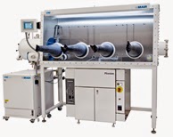
Picosun’s ALD equipment for IMEC is equipped with revolutionary boosting heated source systems and full inert gas glove box integration to enable the best results in coating of moisture sensitive materials with demanding film processes. Picosun’s ALD tools are world known for fulfilling the strictest industrial productivity, film purity, and quality standards scalable to high volume manufacturing with fast process times and low cost-of-ownership.
 
“We are proud of our ALD technology’s continuing expansion to new industrial fields. The fact that IMEC, one of world’s leading semiconductor and nanoelectronics research institutes relies on Picosun’s ALD expertise to enable novel energy storage solutions for global electronic industries speaks volumes about our level of thin film processing know-how and the trust that our customers place on us,” states Juhana Kostamo, Managing Director of Picosun. 
Picosun’s highest level ALD thin film technology enables the industrial leap into the future by novel, cutting-edge coating solutions, with four decades of continuous, groundbreaking expertise in the field. Today, PICOSUN™ ALD systems are in daily production use in numerous major industries around the world. Picosun is based in Finland, with subsidiaries in USA, China, and Singapore, and a world-wide sales and support network.
 
Interesting Links and further reading:
 
The SoS-Lion project at imec to build a functional all solid state 3D thin film microbattery. To this end, both conformal coating processes and solid electrolyte materials need to be developed.
  • Planar thin film battery with focus on conductivity of solid electrolyte
  • 3D thin film battery with focus on conformality and mechanical compliance of solid electrolyte
Towards all solid-state 3D thin-film batteries for durable and fast storage
Article in Solid State Technology by PHILIPPE VEREECKEN, principal scientist, imec, associate professor, KU Leuven

Picosun on Energy storage and production

Wednesday, August 20, 2014

Levitech BV sells ALD system to another Taiwanese solar cell manufacturer

ALMERE, The Netherlands – August 20, 2014 – Levitech BV announces the sale and shipment of a Levitrack® ALD system to a new Taiwanese solar cell manufacturer. This system plays a central role in the development and manufacturing of high-efficiency solar cells on both mono- and multi-crystalline silicon.

In recent years Levitech has supplied a number of Levitrack spatial ALD systems, which deposit aluminum oxide (Al2O3) passivation layers on both p and n-type solar cells, to high-efficiency solar cell manufacturers in Asia. This order marks another step in the market growth and penetration of the aluminum oxide (Al2O3) surface passivation technology and the expansion of Levitech's sales activities.

The Levitrack’s unique spatial ALD process and high throughput result in a superior cost-of-ownership of the overall passivation process flow and helps any client to address current and future technology needs.

About the Levitrack

The Levitrack ALD system is based on the innovative concept of spatial precursor separation, instead of precursor separation in time, and works in combination with the unique floating wafer and conductive heating technology used in the Levitech’s Levitor® RTP products. In the Levitrack, substrates float in a linear gas track and are heated to the required process temperature within a matter of seconds. Once heated, the substrates continue to float through a series of ALD deposition cells. Each cell consists of two precursor ‘curtains’, which are separated by a nitrogen purge ‘curtain’. The unique design of the ALD deposition cells allows for single-side ALD growth. As each ALD deposition cell is optimized for a fast linear motion of the substrates, a high throughput and low cost-of-ownership is guaranteed.

About Levitech

Levitech is a global player in production solutions for the IC and photovoltaic industries. A spin-off of ASM International, Levitech was established in 2009 around its core product, the Levitor® system. This system is based on a revolutionary patented technology and used in the semiconductor industry for Rapid Thermal Processing (RTP). The Levitrack™ ALD system is a state-of-the-art production solution for the solar industry and is based on the innovative concept of precursor separation in space, instead of time, in combination with the unique floating wafer and conductive heating technology used in the Levitor RTP products. For more information, visit Levitech's web site at www.levitech.nl.


Tuesday, August 19, 2014

US-Korean Joint Research Developing New Material Using Atomic Layer-manipulating Tech (MBE)

As reported by Business Korea: A Korean research team has successfully synthesized a new material that can be used in the development of materials in the energy area such as fuel cells, thermal conductors, and superconductors. The Korea Atomic Energy Research Institute (KAERI) announced on August 18 that a Korean research team led by Lee Joon-hyeok, a senior researcher at KAERI, and a U.S. counterpart was able to improve a method for molecular beam deposition that makes nanometer-scale film by stacking up atomic layers one by one.
 
The team also succeeded in synthesizing thin films made of layers of monocrystal lanthanum nickel oxides (Lan+1NinO3n+1 oxides). Since lanthanum nickel oxides have excellent ion conductivity and can respond to catalysts very well, they are actively studied as a material in the energy field like an electrode or a catalyst. In the past, it was difficult to conduct pure research on their characteristics and develop a new material by synthesizing them with other kinds of thin films, because the arrangement of existing polycrystalline lanthanum nickel oxides was irregular. Moreover, the bigger the size, the less regular the material. The joint research team observed in real-time the process where atomic layers of the oxides were piled up, using Oxide Molecular Beam Epitaxy (Oxide MBE) installed in the Advanced Photon Source (APS) Synchrotron at Argonne National Laboratory. During the process, the team discovered the phenomenon of voluntary rearrangement between layers, which means that the order of some atomic layers was not fixed, but reversed instead. By applying this phenomenon, the team manipulated the order that atomic layers of lanthanum oxides and nickel oxides were piled up, and was able to synthesize thin films made of layered compound-type monocrystal lanthanum nickel oxides as a result.
 

a–e, Optimized structures and relative energies of different stackings of two (a,b) or three (c–e) ​SrO and one ​TiO2 layer on a ​TiO2-terminated ​SrTiO3 substrate. (Nature Materials (2014)DOI:doi:10.1038/nmat4039)
 
KAERI is planning to apply the research findings in the development of new materials, such as a change in layer-structure materials and the measurement of material properties, using a neutron reflectometer in the Cold Neutron Research Facility (CNRF). The research findings were first published online on August 3 by Nature Materials.


Sunday, August 17, 2014

Aixtrons OEC-200 cluster platform includes an ALD process module

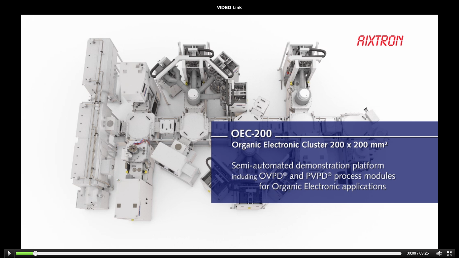
AIXTRON supplies deposition equipment to the semiconductor industry. The company's technology solutions are used by a diverse range of customers worldwide, enabling them to build advanced components for electronic and opto-electronic applications based on compound, silicon, or organic semiconductor materials, for polymers, as well as carbon nanotubes (CNT), graphene and other nanomaterials. For the deposition of organic thin films, AIXTRON offers two core technologies for mass production and R&D: AIXTRON’s Organic Vapor Phase Deposition (OVPD®) equipment serves as enabling technology for the deposition of organic small molecules for OLEDs and organic semiconductor solutions. With its line of Polymer Vapor Phase Deposition (PVPD®) equipment, AIXTRON also offers solutions for carrier gas enhanced vapor phase deposition of functional polymer thin films for a variety of applications, for instance for the manufacturing of functional layers for OTFTs, electro-wetting displays and others. The OVPD-200 system incorporates latest improvements for Organic Vapor Phase Deposition and offers modular source configuration. The new PRODOS-200 provides a powerful evaluation platform for Polymer Vapor Phase Deposition processes. Both solutions can be integrated with the novel OEC-200 cluster platform. Providing a range of integration components such as transfer modules, load locks, buffers, and other subsystems, the OEC-200 platform allows to integrate OVPD -200 and PRODOS-200 into automated cluster environments.”

Aixtron recently relased a video of this Organic Lab at R&D Center OLED Demo Cluster & Gen8 Demo Module. If you watch it you will also notice that it includes an ALD process module!


Aixtrons OEC-200 cluster platform (screendump)


Close up on the ALD process module (screendump) 

Lawrence Livermore researchers have made a super strong material by ALD

Lawrence Livermore researchers have made a material that is 10 times stronger and stiffer than traditional aerogels of the same density. This ultralow-density, ultrahigh surface area bulk material with an interconnected nanotubular makeup could be used in catalysis, energy storage and conversion, thermal insulation, shock energy absorption and high energy density physics.

Ultralow-density porous bulk materials have recently attracted renewed interest due to many promising applications. Unlocking the full potential of these materials, however, requires realization of mechanically robust architectures with deterministic control over form, cell size, density and composition, which is difficult to achieve by traditional chemical synthesis methods, according to LLNL's Monika Biener, lead author of a paper appearing on the cover of the July 23 issue of Advanced Materials.

Biener and colleagues report on the synthesis of ultralow-density, ultrahigh surface area bulk materials with interconnected nanotubular morphology. The team achieved control over density (5 to 400 mg/cm3), pore size (30 um to 4 um) and composition by atomic layer deposition (ALD) using nanoporous gold as a tunable template.

"The materials are thermally stable and, by virtue of their narrow unimodal pore size distributions and their thin-walled, interconnected tubular architecture, about 10 times stronger and stiffer than traditional aerogels of the same density," Biener said.

The three-dimensional nanotubular network architecture developed by the team opens new opportunities in the fields of energy harvesting, catalysis, sensing and filtration by enabling mass transport through two independent pore systems separated by a nanometer-thick 3D membrane.
Monika M. Biener, Jianchao Ye, Theodore F. Baumann, Y. Morris Wang, Swanee J. Shin, Juergen Biener and lex V. Hamza
Adv. Mater. 28/2014, DOI: 10.1002/adma.201470188
 
 
Abstract:
The 3D interconnected nanotubular morphology of ultra-strong, low-density bulk materials derived by atomic layer deposition templating of nanoporous gold is demonstrated by M. M. Biener and co-workers on page 4808. This process provides deterministic control over density, feature size and composition. The unique morphology makes this material stronger and stiffer than other low density materials and opens the door to new filtration and catalysis applications.

Saturday, August 9, 2014

The 3rd Symposium of Atomic Layer Deposition at SEMICON Europa October 7th 2014

Symposium of the ALD-Lab

Workshop on Atomic Layer Deposition

Date: 7 October 2014
Time: 09:00 - 13:00
Location: Room Le Bans, ALPEXPO
 
Organized by:
 
The termination of Moore’s law is often associated with a lack of technological control at atomic dimensions. However the innovative utilization of self limiting heterogeneous chemical reactions enabled the introduction of a new deposition technology into the microelectronic manufacturing process within the last decade, which is generally capable to control film growth within atomic layers on any wafer size and on any topography.
Although the scientific background of ALD goes far back in history ALD can still be considered as an emerging technology. It required challenges like deposition of atomic thin work function layers or novel dielectrics in High-k MG structures to realize the advantage of precise thickness control on large substrates against the low deposition rate that is inherent to ALD.
Progress in ALD is associated with tools, but even more with specifically designed precursors which need to be applied at optimum conditions of the gas feed system, the process chamber and the substrate condition. Our workshop, which is organized by the “ALD Lab Dresden” wants to stimulate discussions between developers of tools, consumables, as well as applicants of this exciting technology.


Agenda

 09:00Welcome and the latest ALD Research at TU Dresden
“Fundamental insight into ALD processing by in-situ observation”
 Johan W. Bartha, Institut für Halbleiter- und Mikrosystemtechnik, TU Dresden, Germany
 
 09:25Development of innovative ALD materials and tools for high density 3D integrated capacitors
Malte Czernohorsky, Fraunhofer IPMS-CNT, Dresden, Germany
 
 09:50Recent Developments in Heteroleptic Chemistries for Next Generation thin films PEALD/ALD
Jean Marc Girard and Nicolas Blasco, Air Liquide Electronics, Paris/Grenoble, France
 
 10:15High permittivity dielectrics for CMOS FDSOI Gate first technologiess
Mickael Gros-Jean, ST Microelectronics, Grenoble, France
 
 10:40ALD deposited ferroelectric HfO2
Stefan Slesazeck, NaMLab, Dresden, Germany
 
 11:05ALD of Metals and Metal Oxides for Advanced Interconnect and Sensor Technology: In-Situ Investigations for the ALD of Copper
Stefan E. Schulz, Fraunhofer ENAS, Chenitz, Germany
 
 11:30Plasma-assisted ALD of Silicon Nitride and Gallium Nitride
Harm C. M. Knoops, Oxford Instruments
 
 11:55Real Time True Surface Monitoring for ALD Processes
Hassan Gargouri, Sentech, Berlin, Germany
 
 12:20Conversation / Networking
 
 13:00Termination of the workshop
 

Registration

No pre-registration required but you must register as a visitor, in order to gain access to the venue:

Thursday, August 7, 2014

Pulsed-bed atomic layer deposition setup for powder coating

An interesting publication on a Pulsed-bed atomic layer deposition setup for powder coating capable of conformal coatings of powders, easy technology for thickness control down to atomic level and a capability to process powders of different characteristics. Find out more in the publication bleow by H. Tizando et al from Universidad Nacional Autónoma de México.

 Pulsed-bed atomic layer deposition setup for powder coating

H. Tiznado, D. Domínguez, F. Muñoz-Muñoz, J. Romo-Herrera, R. Machorro, O.E.
Contreras, G. Soto

Abstract

Atomic layer deposition (ALD) provides a method for coating conformal, pinhole-free, chemically bonded, and ultra-thin films on particle surfaces. ALD is based on one or more cycles, each cycle comprising two half-reactions. As such, ALD is a process inherently discrete in time, where the coating thickness can be controlled as a function of number of cycles. A popular scheme for achieving uniform coats on powders is to combine ALD reactors with fluidization conditions. However, fluidization is not easy to attain because it is strongly dependent on particle size, density, morphology, and surface roughness. This article proposes that a pulsed-bed, instead of a continuous fluidization, is easier to achieve in most ALD reactors. Taking advantage of the discrete nature of the ALD process, with simple changes in the configurations of purge and carrier gases, the pulsed-bed mode can be completed. It is presented an adaptation made to a regular ALD reactor to work in this mode. The inclusion of a capsule for powder, valve relocations, and control of times were all necessary modifications. It was found that the pulsed-bed is a very convenient alternative for research purposes, since it can coat powders of different morphological characteristics, such as carbon nanotubes, flower-like ZnO micro-arrays, and YCrO3 particles.

Lam Research Atomic Layer Etch (ALEt) technology in beta-site evaluations

According to a rescent blog post by Ed Korczynski, Lam Research Atomic-Layer Etch (ALE) technology are in beta-site evaluations.

"Atomic-Layer Etch (ALE) technology from Lam Research Corp. is now in beta-site evaluations with IC fabrication (fab) customers pursuing next generation manufacturing capabilities. So said Dr. David Hemker, Lam’s senior vice president and chief technical officer, in an exclusive interview with Solid State Technology and SemiMD during this year’s SEMICON West trade-show in San Francisco. Hemker discussed the reasons why ALE is now under evaluation as a critically enabling technology for next generation IC manufacturing, and forecast widespread adoption in the industry by 2017."


Commonality in the need for ALD and ALE process technologies when IC device dimensions scale to atomic levels.

"As detailed in the feature article “Moving atomic layer etch from lab to fab” in last December’s issue of Solid State Technology, ALE can be plasma enhanced with minor modifications to a continuous plasma etch chamber. The lab aspects including the science behind the process were discussed in a TechXPOT during SEMICON West this year in a presentation titled “Plasma Etch in the Era of Atomic Scale Fidelity” by Lam’s Thorsten Lill based on work done in collaboration with KU Leuven and imec. In that presentation, Lill reminded the attendees that the process has been explored in labs under a wide variety of names: ALET, atomistic etching, digital etch, layer-by-layer etch, PALE, PE-ALE, single layer etch, and thin layer etching."
 
Full store here.

Reflectionless Transmission through Dielectrics by ALD

As reported by The Times of India: Three-year-long targeted research by Tata Institute of Fundamental Research team led by Professor Achanta Venu Gopal with design and simulation input from a senior optics faculty at University of Hyderabad, Professor S Dutta Gupta, has led to the experimental confirmation of a US patent (no: US 7,894,137 B2).
 
The patent is jointly owned by UoH and Oklahoma State University (OSU), with inventors Professor S Dutta Gupta (UoH) and Prof. Girish Agarwal (OSU) and deals with complete transparency of a graded index dielectric film based on the concept of reflectionless potentials. The notion of reflectionless potentials was proposed by Kay and Moses (I. Kay and H. E. Moses, "Reflectionless transmission through dielectrics and scattering potentials," J. Appl.Phys. 27(12), 1503-1508 (1956)). It was extensively used in inverse scattering and high energy physics theory. Incidentally there were very few research efforts in optics.
 
I. Kay and H. E. Moses, "Reflectionless transmission through dielectrics and scattering potentials," J. Appl.Phys. 27(12), 1503-1508 (1956)).
 
The realization of the optical reflectionless potential opens up new directions for a totally new design methodology for omnidirectional broadband optical coatings to enhance the throughput of any optical device. Note that standard antireflection coatings mostly makes use of quarter wavelength plates, and thus cannot be broadband and omnidirectional. The realisation of optical reflectionless potentials was a real experimental challenge in the context of choice of materials and finding the optimal technique. The graded reflectionless profile was achieved with Titanium and Aluminium oxide nano layers since they have high and low refractive indices, respectively, and a proper combination can lead to an effective medium with intermediate desired refractive index.

"We had to explore different layer deposition techniques since nanometer thick layers needed for the profile have different optical properties depending on the technique. We had to use techniques ranging from atomic layer deposition, electron beam evaporation to sputtering. We are still in the process of refining the growth process", says Prof. Gopal.
 
There are other fundamentally interesting properties like superluminal group velocities, pulse narrowing etc., which are being probed. Note that superluminal group velocities do not violate Einstein's principles, since the peaks of the emerging and incident pulses are not causally related.

Tuesday, August 5, 2014

Cornell - The perfect atom sandwich requires an extra layer

As reported by Cornell: Cornell researchers have discovered that sometimes, layer-by-layer atomic assembly – a powerful technology capable of making new materials for electronics – requires some unconventional “sandwich making” techniques.

The team, led by thin-films expert Darrell Schlom, the Herbert Fisk Johnson Professor of Industrial Chemistry in the Department of Materials Science and Engineering, describes the trick of growing perfect films of oxides called Ruddlesden-Poppers in Nature Communications Aug. 4.
 
The left figure demonstrates why the first double layer of strontium oxide is missing when growing a Ruddlesden-Popper oxide thin film. Titanium atoms (yellow) preferentially bond with oxygen atoms (gray) and sit at the center of a complete octahedron, making it energetically more favorable for titanium to switch positions with the topmost strontium oxide layer (red). Because of this, the first double layer of strontium oxide is always missing, and the extra layer rides the surface. By depositing an extra strontium oxide layer first, the desired first double layer is obtained. (source : Cornell)

These oxides are widely studied for their electronically enticing properties, among them superconductivity, magnetoresistance and ferromagnetism. Their layered structure is like a double Big Mac with alternating double and single layers of meat patties – strontium oxide – and bread – titanium oxide – in the case of the Ruddlesden-Poppers studied.

“Our dream is to control these materials with atomic precision,” Schlom said. “We think that controlling interfaces between Ruddlesden-Poppers will lead to exotic and potentially useful, emergent properties.”

Schlom’s lab makes novel thin films with molecular beam epitaxy, a deposition method that controls the order in which atom-thick layers are assembled layer-by-layer, which Schlom likens to precision spray-painting with atoms.
Full story here and Nature abstract below.
 
Atomically precise interfaces from non-stoichiometric deposition
Y. F. Nie, Y. Zhu, C.-H. Lee, L. F. Kourkoutis, J. A. Mundy, J. Junquera, Ph. Ghosez, D. J. Baek, S. Sung, X. X. Xi, K. M. Shen, D. A. Muller & D. G. Schlom   
Nature Communications 5, Article number: 4530, 04 August 2014
     
Complex oxide heterostructures display some of the most chemically abrupt, atomically precise interfaces, which is advantageous when constructing new interface phases with emergent properties by juxtaposing incompatible ground states. One might assume that atomically precise interfaces result from stoichiometric growth. Here we show that the most precise control is, however, obtained by using deliberate and specific non-stoichiometric growth conditions. For the precise growth of Srn+1TinOn+1 Ruddlesden–Popper (RP) phases, stoichiometric deposition leads to the loss of the first RP rock-salt double layer, but growing with a strontium-rich surface layer restores the bulk stoichiometry and ordering of the subsurface RP structure. Our results dramatically expand the materials that can be prepared in epitaxial heterostructures with precise interface control—from just the n=∞ end members (perovskites) to the entire RP homologous series—enabling the exploration of novel quantum phenomena at a richer variety of oxide interfaces.


Monday, August 4, 2014

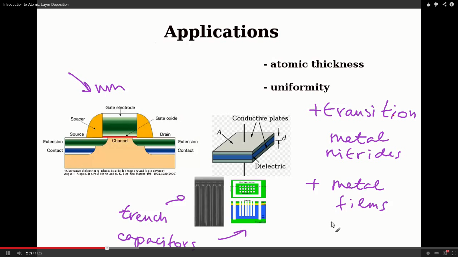
New Atomic Layer Deposition (ALD) educational video

A new Atomic layer deposition educational video Image and information sources:

"Atomic Layer Deposition of Nanostructured Materials". WILEY_VCH, ed. N. Pinna and M. Knez
"Atomic Layer Deposition: Principles, Characteristics, and Nanotechology Applications", 2ed, T. Kaarlainen, D. Cameron, M.-L. Kaarlainen, A. Sherman (2013)
S. Narasimha, IEDM 2012 pp. 52-55
wikimedia commons

 
 Screendump from the video (youtube.com)


Edwards on the need for Vacuum Technologies for ALD and 3D Device Processing

A very interesting blog post on the need for Vacuum Technologies for ALD and 3D Device Processing. Thanks Toni Koblenz for the tip on this one!

Future ICs will use more 3D device structures such as finFETs and gate-all-around (GAA) transistors, and so vacuum deposition processes are needed that can produce conformal films on the tops, bottoms, and side-walls of features. New materials are needed as the commercial IC fabrication industry pushes the limits of device miniaturization, while industry consolidation drives the remaining players to use proprietary materials.

Even lithography needs more vacuum processing when double-, triple-, and quadruple-patterning schemes need sidewall spacer and sacrificial hard-mask depositions. Materials deposited in these process steps may not remain on the final chip, but they are nonetheless essential in sub-22nm node process flows.

All of this leads to a need for an unprecedented number of new chemical precursors for vacuum depositions to be simultaneously ramped into high-volume manufacturing (HVM) in fabs worldwide. “If you’re trying to deposit a metal nitride, for example, four different fabs may use four different precursors sets,” explained Kate Wilson, global applications director, Edwards Vacuum Ltd. in an exclusive interview with the Show Daily.
 
 
Pulsed precursors in a vacuum system.

For some ALD process there are conflicting challenges in configuring a vacuum solution, such as one using a MOCVD precursors and a chloride precursor. For the MOCVD molecule the general approach would be to lower temperatures to prevent decomposition, while for the chloride molecule it would be best to use high temperatures to prevent condensation. Some molecules polymerize more at higher temperatures, while condensing more at lower temperatures, so a strategic trade-off must be made.

“Chlorine-based precursors, for example, are quite challenging to abate without creating toxic by-products,” explained Wilson. “Most of the things we abate become a powder, so we have to deal with that powder to ensure that we don’t clog the system.”

Saturday, August 2, 2014

Capillary flow layer-by-layer (CF-LbL) employed by MIT researchers for fast screening of films

Capillary flow layer-by-layer (CF-LbL) - An very interesting publication (ACS Nano, 2014, 8 (7), pp 6580–6589) from Massachusetts Institute of Technology (MIT) on liquid Layer-by Layer growth in a combinatorial approach for fast screening of thin films.

Capillary Flow Layer-by-Layer: A Microfluidic Platform for the High-Throughput Assembly and Screening of Nanolayered Film Libraries
Steven A. Castleberry, Wei Li, Di Deng, Sarah Mayner, and Paula T. Hammond
 
ACS Nano, 2014, 8 (7), pp 6580–6589, DOI: 10.1021/nn501963q


Abstract: Layer-by-layer (LbL) assembly is a powerful tool with increasing real world applications in energy, biomaterials, active surfaces, and membranes; however, the current state of the art requires individual sample construction using large quantities of material. Here we describe a technique using capillary flow within a microfluidic device to drive high-throughput assembly of LbL film libraries. This capillary flow layer-by-layer (CF-LbL) method significantly reduces material waste, improves quality control, and expands the potential applications of LbL into new research spaces. The method can be operated as a simple lab benchtop apparatus or combined with liquid-handling robotics to extend the library size. Here we describe and demonstrate the technique and establish its ability to recreate and expand on the known literature for film growth and morphology. We use the same platform to assay biological properties such as cell adhesion and proliferation and ultimately provide an example of the use of this approach to identify LbL films for surface-based DNA transfection of commonly used cell types.

Friday, August 1, 2014

Perovskite pseudocapacitors for energy storage from Texas

Anion charge storage through oxygen intercalation in LaMnO3 perovskite pseudocapacitor electrodes

J. Tyler Mefford, William G. Hardin, Sheng Dai, Keith P. Johnston and Keith J. Stevenson
Nature Materials Volume: 13, Pages: 726–732 01 June 2014 


Abstract

Perovskite oxides have attracted significant attention as energy conversion materials for metal–air battery and solid-oxide fuel-cell electrodes owing to their unique physical and electronic properties. Amongst these unique properties is the structural stability of the cation array in perovskites that can accommodate mobile oxygen ions under electrical polarization. Despite oxygen ion mobility and vacancies having been shown to play an important role in catalysis, their role in charge storage has yet to be explored. Herein we investigate the mechanism of oxygen-vacancy-mediated redox pseudocapacitance for a nanostructured lanthanum-based perovskite, LaMnO3. This is the first example of anion-based intercalation pseudocapacitance as well as the first time oxygen intercalation has been exploited for fast energy storage. Whereas previous pseudocapacitor and rechargeable battery charge storage studies have focused on cation intercalation, the anion-based mechanism presented here offers a new paradigm for electrochemical energy storage.


Thursday, July 31, 2014

Nanofabrication on bumpy or multilevel surfaces using ALD presented by Aalto University

Nanofabrication on bumpy or multilevel surfaces is often a problem; even for the most accurate state-of-the-art methods. Now, reporting in Nanotechnology, researchers at Aalto University in Finland have established a rapid fabrication process that may provide a solution. They utilize atomic layer deposition (ALD) of ion-sensitive resist for the very conformal coating of non-planar sample surfaces. The key feature is the exposure of patterns by focussed ion beam (FIB), which has a large depth of focus in comparison to e-beam or UV lithographies.
 
 
The application of ALD and FIB effectively solves the problems with resist deposition and exposure. The difficulties associated with non-uniform etching speed are addressed by solely utilizing dry etching for both the resist development and release etching steps.


Revolutionary microshutter technology by NASA improved ALD

NASA technologists have hurdled a number of significant technological challenges in their quest to improve an already revolutionary observing technology originally created for the James Webb Space Telescope.


The team, led by Principal Investigator Harvey Moseley, a scientist at NASA’s Goddard Space Flight Center in Greenbelt, Maryland, has demonstrated that electrostatically actuated microshutter arrays — that is, those activated by applying an specific voltage — are as functional as the current technology’s magnetically activated arrays. This advance makes them a highly attractive capability for potential Explorer-class missions designed to perform multi-object observations.
“We have identified real applications — three scientists want to use our microshutter arrays and the commercial sector has expressed interest,” said Mary Li, a Goddard engineer who is working with Moseley and other team members to fully develop this already groundbreaking observing technology. “The electrostatic concept has been fully demonstrated and our focus now is on making these devices highly reliable.”

[...]

Through experimentation, the team used atomic layer deposition, a state-of-the-art fabrication technology, to fully insulate the tiny space between the electrodes to eliminate potential electrical crosstalk that could interfere with the arrays’ operation.

Full story as reported by NASA here.

Wednesday, July 30, 2014

MIT present self-assembly of ALD functionalised carbon nanotubes

A team of researchers at MIT has presented a new way to make microstructured surfaces - A method can produce strong, lightweight materials with specific surface properties. by employing ALD coatings. The team has created a new way of manufacturing microstructured surfaces that have novel three-dimensional textures. These surfaces, made by self-assembly of carbon nanotubes, could exhibit a variety of useful properties — including controllable mechanical stiffness and strength, or the ability to repel water in a certain direction.

“We have demonstrated that mechanical forces can be used to direct nanostructures to form complex three-dimensional microstructures, and that we can independently control … the mechanical properties of the microstructures,” says A. John Hart, the Mitsui Career Development Associate Professor of Mechanical Engineering at MIT and senior author of a paper describing the new technique in the journal Nature Communications.

The technique works by inducing carbon nanotubes to bend as they grow. The mechanism is analogous to the bending of a bimetallic strip, used as the control in old thermostats, as it warms: One material expands faster than another bonded to it. But in this new process, the material bends as it is produced by a chemical reaction.
 
 
Close-up microscope images of carbon nanotube forms and illustrations of the patterns that produce them. At left, a simple curved form, and at right, complex curved propeller shapes, that can be produced by this carbon nanotube growth method. (MIT News)


The process begins by printing two patterns onto a substrate: One is a catalyst of carbon nanotubes; the second material modifies the growth rate of the nanotubes. By offsetting the two patterns, the researchers showed that the nanotubes bend into predictable shapes as they extend.

“We can specify these simple two-dimensional instructions, and cause the nanotubes to form complex shapes in three dimensions,” says Hart. Where nanotubes growing at different rates are adjacent, “they push and pull on each other,” producing more complex forms, Hart explains. “It’s a new principle of using mechanics to control the growth of a nanostructured material,” he says.

Few high-throughput manufacturing processes can achieve such flexibility in creating three-dimensional structures, Hart says. This technique, he adds, is attractive because it can be used to create large expanses of the structures simultaneously; the shape of each structure can be specified by designing the starting pattern. Hart says the technique could also enable control of other properties, such as electrical and thermal conductivity and chemical reactivity, by attaching various coatings to the carbon nanotubes after they grow.

“If you coat the structures after the growth process, you can exquisitely modify their properties,” says Hart. For example, coating the nanotubes with ceramic, using a method called atomic layer deposition, allows the mechanical properties of the structures to be controlled. “When a thick coating is deposited, we have a surface with exceptional stiffness, strength, and toughness relative to [its] density,” Hart explains. “When a thin coating is deposited, the structures are very flexible and resilient.”

This approach may also enable “high-fidelity replication of the intricate structures found on the skins of certain plants and animals,” Hart says, and could make it possible to mass-produce surfaces with specialized characteristics, such as the water-repellent and adhesive ability of some insects. “We’re interested in controlling these fundamental properties using scalable manufacturing techniques,” Hart says.

Hart says the surfaces have the durability of carbon nanotubes, which could allow them to survive in harsh environments, and could be connected to electronics and function as sensors of mechanical or chemical signals.

Kevin Turner, an associate professor of mechanical engineering and applied mechanics at the University of Pennsylvania who was not involved in this research, says this approach “is quite novel because it allows for the engineering of complex 3-D microstructures [composed] of carbon nanotubes. Traditional microfabrication approaches, such as patterning and etching, generally only allow for the fabrication of simple 3-D structures that are essentially extruded 2-D patterns.”

Turner adds, “A particularly exciting aspect of this work is that the structures are composed of carbon nanotubes, which have desirable mechanical, thermal, and electrical properties.”

Along with Hart, the research team included Michael de Volder of Cambridge University; Sei Jin Park, a visiting doctoral student from the University of Michigan; and Sameh Tawfick, a former postdoc at MIT who is now at the University of Illinois at Urbana-Champaign. The work was supported by the European Research Council, the Defense Advanced Research Projects Agency, and the Air Force Office of Scientific Research.

Tuesday, July 29, 2014

VIDEO : An overview on Atomic Layer Etching (ALEt) from Stanford

VIDEO : An overview on Atomic Layer Etching (ALEt)  created for Stanford Nanomanufacturing Class July 2014. Thanks Annina at ALDPulse.com for sharing this!
 
 
Screendump - explaining self aligned double pattering (SAPD) and cration of silicon fins for leading edge FinFETs.


Video on ALEt as published on Youtube.com

Wednesday, July 23, 2014

ECS JSS Special issue on Atomic Layer Etch (ALEt) and Atomic Layer Clean (ALC)

As announced by JSS : Atomic Layer Etch (ALEt) and Atomic Layer Clean (ALC) are emerging as enabling technologies for sub 10nm technology nodes. At these scales performance will be extremely sensitive to process variation. Novel technologies will be required to control variation without increasing complexity if successful introduction of ALEt and ALC into manufacturing schemes is to be achieved. At even more aggressive nodes where novel 2D materials are being considered, the need for zero damage and quasi-infinite selectivity to underlying films or substrates becomes increasingly important.
                          
Atomic layer processes are the most promising path to deliver the precision needed at this scale. However, many areas of ALEt and ALC are in need of improved fundamental understanding and process development. This focus issue will cover state-of-the-art efforts that address a variety of approaches to ALE and ALC. Specific topics of interest include but are not limited to:
  • Surface reaction chemistry and its impact on selectivity
  • Plasma ion energy distribution and control methods
  • Novel plasma sources and potential application to ALEt & ALC
  • Innovative approaches to atomic layer material removal
  • Novel device applications of ALEt & ALC
  • Process chamber design considerations
  • Advanced delivery of chemicals to processing chambers
  • Metrology and control of ALEt & ALC
  • Device performance impact
  • Synthesis of new chemistries for ALEt & ALC application
  • Damage free surface defect removal
  • Process and discharge modeling


Submission Deadline: Dec. 17, 2014

Please submit manuscripts at http://ecsjournals.msubmit.net
Please be sure to specify your submission is for the JSS Focus Issue on
Atomic Layer Etching and Cleaning


Guest Editors:
Dennis Hess
dennis.hess@chbe.gatech.edu
Stefan De Gendt
stefan.degendt@imec.be
Craig Huffman
craig.huffman@sematech.org
Jean-Francois de Marneffe
jean-francois.demarneffe@imec.be
Makoto Sekine
sekine@plasma.engg.nagoya-u.ac.jp

Tuesday, July 22, 2014

Riber signs distribution agreement with CVD & ALD firm AnnealSys

As reported by Semiconductor Today: Riber S.A. of Bezons, France, which manufactures molecular beam epitaxy (MBE) systems as well as evaporation sources and effusion cells, has signed a distribution agreement with AnnealSys SAS of Montpellier, France, which specializes in vapour-phase chemical deposition processes.

The Annealsys MC050 is a 2-inch multi process system (DLI-CVD, DLI-ALD, MOCVD, RTP and RTCVD) offering the widest capabilities for development of new materials (source AnnealSys.com).
 

AnnealSys designs and produces rapid thermal annealing (RTA) furnaces and chemical vapour deposition (CVD) and atomic layer deposition (ALD) systems, which make it possible to deposit complex materials for a wide range of applications, from semiconductors to solar cells, LEDs and microsystems.

AnnealSys’ equipment is aimed primarily at research laboratories and universities, while also meeting the needs of industrial operators for producing small batches. Founded in 2004, the firm has built up unique CVD and ALD expertise, particularly for the integration of direct liquid injection vaporizers, making it possible to implement a wide variety of chemical precursors and to develop processes for growing new materials.

Initially, the partnership between Riber and AnnealSys will focus on CVD and ALD products and the American and Asian regions.

With this commercial agreement, AnnealSys is aiming to accelerate its sales growth internationally by capitalizing on Riber’s sales capabilities and reputation in the research community.

Riber says the agreement represents an opportunity for it to continue moving forward with its technical diversification into other thin-film deposition techniques. The firm says that the commercial partnership will strengthen the range of equipment and services that it offers. The development is also in line with the diversification strategy presented to shareholders at the latest general meeting.
 

Monday, July 21, 2014

'Nano-pixels' promise thin, flexible high-res displays by phase-change films

University of Oxford reports - A new discovery will make it possible to create pixels just a few hundred nanometres across that could pave the way for extremely high-resolution and low-energy thin, flexible displays for applications such as 'smart' glasses, synthetic retinas, and foldable screens.


Still images drawn with the technology: at around 70 micrometres across each image is smaller than the width of a human hair. (Source, University of Oxford)
 
A team led by Oxford University scientists explored the link between the electrical and optical properties of phase change materials (materials that can change from an amorphous to a crystalline state). They found that by sandwiching a seven nanometre thick layer of a phase change material (GST) between two layers of a transparent electrode they could use a tiny current to 'draw' images within the sandwich 'stack'.

Initially still images were created using an atomic force microscope but the team went on to demonstrate that such tiny 'stacks' can be turned into prototype pixel-like devices. These 'nano-pixels' – just 300 by 300 nanometres in size – can be electrically switched 'on and off' at will, creating the coloured dots that would form the building blocks of an extremely high-resolution display technology.
 

Schematic representation of the thin-film material stack comprising ITO/GST/ITO.

Continue reading:  http://www.ox.ac.uk/news/2014-07-10-nano-pixels-promise-thin-flexible-high-res-displays# and a report of the research has been published in this week's Nature.

Also EE Times has more on this story here.

Sunday, July 13, 2014

Ferroelectric deep trench capacitors based on Al:HfO2 for 3D nonvolatile memory applications

P. Polakowski, S. Riedel, W. Weinreich, M. Rudolf, J. Sundqvist, K. Seidel, J. Muller
Memory Workshop (IMW), 2014 IEEE 6th International
Date of Conference: 18-21 May 2014 Page(s): 1 - 4 Print ISBN: 978-1-4799-3594-9 Conference Location : Taipei, Taiwan DOI:10.1109/IMW.2014.6849367
 
Aiming for future nonvolatile memory applications the fabrication and electrical characterization of 3-dimensional trench capacitors based on ferroelectric HfO2 is reported. It will be shown that the ferroelectric properties of Al-doped HfO2 ultrathin films are preserved when integrated into 3-dimensional geometries. The Al:HfO2 thin films were deposited by ALD and electrical data were collected on trench capacitor arrays with a trench count up to 100k. Stable ferroelectric switching behavior was observed for all trench arrays fabricated and only minimal remanent polarization loss with increasing 3-dimensional area gain was observed. In addition these arrays were found to withstand 2∗109 endurance cycles at saturated hysteresis loops. With these report the 3D capability of ferroelectric HfO2 is confirmed and for the first time a feasible solution for the vertical integration of ferroelectric 1T/1C as well as 1T memories is presented.
 

Process flow scheme for the fabricated ferroelectric deep trench capacitors with high aspect ratio of 13:1 and the accordingly measured hysteresis loop of a 3D deep trench capacitor


IBM Zürich solves 40+ Year Old Challenge for Phase Change Materials

IBM Research reports in their News Blog on a breakthrough made in understanding and development of phase change memory cells by IBM Research in Zürich. "... for more than 40 years scientists have never measured the temperature dependence of crystal growth, due to the difficulties associated with the measurements which are taken at both a nanometer length and a nanosecond time scale. That was until earlier this year when, for the first time, IBM scientists in Zurich were able to take the measurements, which is today being reported in the peer-review journal Nature Communications."
 
 
The Binnig and Rohrer Nanotechnology Center is a unique facility for exploratory research. It is not a production or a pilot line with fixed processes or wafer sizes. Rather, it is a state-of-the-art exploratory cleanroom fabrication facility combined with "noise-free" labs shielded against external vibrations, acoustic noise, electromagnetic fields and temperature fluctuations.
 
Please see the abstract to the publication below and check out the blog more details including also an interview with the resreachers at The Binnig and Rohrer Nanotechnology Center in Zürich.
 
  
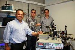
Abu Sebastian, Manuel Le Gallo und Daniel Krebs (Bild: IBM Research)

Abu Sebastian, Manuel Le Gallo, & Daniel Krebs,
Nature Communications Volume: 5, Article number: 4314 DOI:doi:10.1038/ncomms5314, 07 July 2014

In spite of the prominent role played by phase change materials in information technology, a detailed understanding of the central property of such materials, namely the phase change mechanism, is still lacking mostly because of difficulties associated with experimental measurements. Here, we measure the crystal growth velocity of a phase change material at both the nanometre length and the nanosecond timescale using phase-change memory cells. The material is studied in the technologically relevant melt-quenched phase and directly in the environment in which the phase change material is going to be used in the application. We present a consistent description of the temperature dependence of the crystal growth velocity in the glass and the super-cooled liquid up to the melting temperature.
 
 
The cross-sectional tunneling  electron microscopy (TEM) image of  a mushroom-type PCM cell  is shown in this photo.
 

Saturday, July 12, 2014

Self assembly of 15,000 semiconductor chips per hour

The Next Big Future Blog reports on a A first automated reel-to-reel fluidic self-assembly process for macroelectronic applications. The system enables high speed assembly of semiconductor dies (15,000 chips per hour using a 2.5 cm wide web) over large area substrates. The optimization of the system (hour 99% assembly yield) is based on identification, calculation, and optimization of the relevant forces. As an application the production of a solid state lighting panel is discussed involving a novel approach to apply a conductive layer through lamination.

A First Implementation of an Automated Reel-to-Reel Fluidic Self-Assembly Machine 
Se-Chul Park , Jun Fang , Shantonu Biswas , Mahsa Mozafari , Thomas Stauden , and Heiko O. Jacobs
Adv. Mater. 2014, DOI: 10.1002/adma.201401573 (Free down load)

In this communication, we report on recent progress towards a fi rst implementation of a self-assembly machine that is based on surface-tension-directed-self-assembly. The reported assembly process is no longer a discontinuous smallbatch hand-operated process but resembles an automated machine like process involving a conveyer belt and a reel-to-reel (RTR) type assembly approach with automated agitation. As a comparison, the assembly rate of conventional chip level pick-and-place machines depends on the cost of the system and number of assembly heads that are used. For example, a highend FCM 10000 (Muehlbauer AG) fl ip chip assembly system can assemble approximately 8000 chips per hour achieving a placement accuracy of 30 μm. 

Our current design achieves 15 k chips per hour using a 2.5 cm wide assembly region which is only a factor of 2 better than one of the faster pick-and-place machines; scaling to 150 k chips per hour, however, would be possible using a 25 cm wide web, which would be a factor of 20 faster. 


In principle, scaling to any throughput should be possible considering the parallel nature of self-assembly. In terms of placement accuracy our precision increase with a reduction of chip and solder bump size. Generally, it exceeds the 30 μm limits for the components that have been used. Under optimized operational conditions, we achieved an assembly yield of 99.8% using the self-assembly process. As an application the assembly machine is applied to the realization of area lighting panels incorporating distributed inorganic light emitting diodes (LEDs).


Friday, July 11, 2014

IBM is investing $3 billion to push the limits of chip technology to 7 nm and beyond

Nanowerk News reports: IBM today announced it is investing $3 billion over the next 5 years in two broad research and early stage development programs to push the limits of chip technology needed to meet the emerging demands of cloud computing and Big Data systems. These investments will push IBM's semiconductor innovations from today's breakthroughs into the advanced technology leadership required for the future.


IBM infoographic

Peeling back the layers of thin film structure and chemistry

Nanowerk News reports: Perovskites — any material with the same structure as calcium titanium oxide (CaTiO3) —continue to entice materials scientists with their ferroelectricity, ferromagnetism, catalytic activity, and oxygen-ion conductivity. In recent years, scientists realized that they could vastly improve the properties of perovskites by assembling them into thin films. The problem was that no one understood why thin films beat out bulk materials.Researchers gained new insight into thin-film superiority by probing the structure of perovskites at the X-ray Science Division 33-ID-D,E x-ray beamline at the U.S. Department of Energy's Advanced Photon Source (APS), Argonne National Laboratory. They used a groundbreaking approach to tease apart the thin-film structure and chemistry layer-by-layer

Read more: Peeling back the layers of thin film structure and chemistry http://www.nanowerk.com/nanotechnology-news/newsid=36506.php#ixzz37BBtO4pz 


                                              Graphical abstract: Revealing the atomic structure and strontium distribution in nanometer-thick La0.8Sr0.2CoO3−δ grown on (001)-oriented SrTiO3


Zhenxing Feng, Yizhak Yacoby, Wesley T. Hong, Hua Zhou, Michael D. Biegalski, Hans M. Christen and Yang Shao-Horn

Surface segregation in metal oxides can greatly influence the oxygen transport and surface oxygen exchange kinetics critical to the performance of solid-state devices such as oxygen permeation membranes and solid oxide fuel/electrolytic cell electrodes. Unfortunately detecting elemental distributions at the atomic scale near the surface remains challenging, which hampers the understanding of underpinning mechanisms and control of surface segregation for the design of high-performance materials. Using the coherent Bragg rod analysis (COBRA) method, we report the first direct 3D atomic imaging of a 4 nm-thick “La0.8Sr0.2CoO3–δ”/SrTiO3epitaxial film. Of significance, energy differential COBRA revealed pronounced Sr segregation (La1−xSrxCoO3−δ, x 0.4) in the four unit cells from the top surface while complete Sr depletion was detected in the five unit cells from the “La0.8Sr0.2CoO3−δ”/SrTiO3 interface. The drastic strontium compositional changes in the film were associated with large changes in the atomic positions of apical oxygen sites in the perovskite structure. Such Sr segregation tendencies toward the surface were also found in nominal “La0.6Sr0.4CoO3−δ” thin films, which can greatly enhance the surface oxygen exchange properties of oxides. The results presented here show that COBRA and the differential COBRA methods can be used to investigate a variety of electrochemically active systems providing atomic scale structural and chemical information that can help understand the physical and chemical properties of these systems and serve as a basis for comparison with DFT calculations.


Tuesday, July 8, 2014

VIDEO from Lam Research - Engineering at the Atomic Scale ALD & ALE

Cool video from the Lam Reaearch blog - Building Chips a Few Atoms at a Time


Snap shot from the animated video below (youtube.com)

"Atomic layer deposition (ALD) and atomic layer etch (ALE) use cycles of multi-step processes to deposit or remove a few atomic layers at a time, providing chipmakers with the process control needed for next-generation device manufacturing. To see how these technologies work, check out our latest video"

HAM-LET is releasing its new Ultra Fast (UF) Diaphragm Valve for ALD

HAM-LET is releasing its new Ultra Fast (UF) Diaphragm Valve for Atomic Layer Deposition and fast switching applications, at Semicon West in San Francisco, booth no. 1539, from 8-10 July.

"Our UF's unique flow adjustment mechanism, patent pending no. US 61/910,79, allows for exceptional flow tuning during operation," said Eran Pintel, VP Marketing and Sales at HAM-LET.


"Another advantage of our UF diaphragm valve is its outstanding durability and low maintenance, as it offers over 100 million life cycles. The UF series meets the demand for high-precision diaphragm valves that can perform accurately and repeatedly over an extremely large number of cycles, required by ALD applications," said Pintel.

The optional extended bonnet and cooling fin provide a superb solution when precise and repeatable performance in high-temperature applications is required. The UF series offers superior sealing performance and remarkable durability in hazardous environments, under severe demands of ultra fast actuation at high purity applications.

HAM-LET will showcase a live demonstration of the UF series at Semicon West 2014, booth no. 1539.

About HAM-LET Group

Founded in 1950, HAM-LET Group specializes in the design, development production and marketing of high quality instrumentation valves and fittings in a wide variety of materials for high pressure, high temperature and vacuum applications. An accent on quality combined with ongoing research and development has given the company an international reputation for excellence. As a result, HAM-LET Group today is the fastest growing company in this industry. We are Totally Committed to our customers providing highest quality products and best of breed service. Our products are used around the world in a wide range of industries, including Energy, Oil & Gas, Ground Turbines, Chemical and Petrochemical, CNG/NGV, Semiconductor, Analytical and others.

Visit us at: http://www.ham-let.com

Imec Achieve Record for n-PERT Solar Cell with Spatial ALD from SoLayTec

As reported today : Nano-electronics research center Imec, reported today an n-type PERT crystalline silicon (Si) solar cell fabricated on a large area wafer (15.6cm x 15.6 cm) reaching a top conversion efficiency of 21.5%(calibrated at ISE CalLab), claiming that this is the highest efficiency achieved for this type of solar cell on an industrial large area wafer size.

This result will accelerate the adoption of n-type PERT (Passivated Emitter, Rear Totally diffused) solar cells in the industry as it clearly shows the potential for improved conversion efficiencies for next generation standard two side contacted crystalline silicon solar cells. Additionally imec researchers showed recently that n-type PERT solar cells of imec, having a rear emitter, are not affected by reliability risks originating from a front Ni/Cu plated metallization.

The cell reaching this 21.5% conversion efficiency had an open circuit voltage (Voc) of 677mV, a short circuit current (Jsc) of 39.1 mA/cm2, and 81.3% fill factor, and features a rear blanket p+ emitter obtained by boron diffusion. Reliable front metal contacts on an n+ front-surface-field are formed by means of Ni/Cu/Ag plating (3 bus bars grid) using an industrial plating tool from Meco, while the rear local contacts to the p+ emitter were obtained by laser ablation of the rear passivation stack and subsequent physical-vapor-deposition of aluminum. The rear passivation stack includes a thin (<10 nm) Atomic-Layer-Deposited (ALD) Al2O3 layer, deposited with the spatial ALD technique InPassion Lab from SoLayTec.

The adoption of ALD Al2O3 based-passivation for the p+ emitter resulted in an average improvement in cell efficiency of about 0.3% absolute with respect to passivation by wet oxidation. This illustrates the excellent capabilities of ALD for passivation layers in next generation cell concepts like PERC and n-type PERT.

These results have been achieved in the framework of the imec’s industrial affiliation program on advanced silicon solar cells, dedicated to developing high performance and low cost Si PV-technologies. In this program, imec works closely together with industrial and academic partners along the solar cell value chain. Via participation and contribution to this program, these partners support Imec’s developments and obtain early access to new technology solutions in this way accelerating their own product development.


Lam's New Products Deliver Critical Capability for Building 3D NAND Memory Devices

As reported today by Lam Research Corp. : Lam Research Corp. today unveiled its latest thin film deposition and plasma etch products for 3D NAND fabrication. As memory customers begin ramping production of these new devices, greater process control is needed for cost-effective manufacturing. Lam's new systems address this need for three of the most critical steps in forming 3D NAND memory cells: stack deposition (VECTOR® Q Strata(tm)), vertical channel etching (2300® Flex(tm) F Series), and tungsten wordline deposition (ALTUS® Max ICEFill(tm)).


The 3D NAND memory structures now moving to production involve numerous pairs of stacked films. Process variability on both the horizontal and vertical planes must be minimized for critical steps so that each memory cell in the final device delivers similar performance. Otherwise, variation in one step can be transferred and multiplied in subsequent steps, compounding errors and leading to poor device performance and low product yield. With 40 or more pairs of films in the stack, carefully managing even slight process fluctuations is essential. Lam's new products address these stringent control requirements.

As memory customers begin ramping production of these new devices, greater process control is needed for cost-effective manufacturing. Lam's new systems address this need for three of the most critical steps in forming 3D NAND memory cells: stack deposition (VECTOR® Q Strata™), vertical channel etching (2300® Flex™ F Series), and tungsten wordline deposition (ALTUS® Max ICEFill™).


The new VECTOR Q Strata PECVD (plasma enhanced chemical vapor deposition) system is used for depositing multilayer film stacks. For this critical 3D NAND process step, the system can perform both oxide/nitride (ONON) and oxide/polysilicon (OPOP) film stack deposition. To deposit the ultra-smooth, uniform films required to avoid compounding errors, the system's matched chambers deliver superior defectivity, film stress, and wafer bow performance. In addition, the VECTOR Q Strata also provides industry-leading productivity with the highest throughput per square meter of fab area available today. As the number of layers in these stacks continues to grow, high productivity is increasingly important for cost-effective production.

Once the stack of paired films is deposited, Lam's 2300 Flex F Series dielectric etch product is used to create a vertical channel through the stack. The new system can etch through high aspect ratio structures with minimal distortion or sidewall damage, while also tightly controlling etch profile uniformity across the wafer. This capability is critical since even small deviations can cause channel dimensions to differ from cell to cell, resulting in device performance variation. A proprietary high ion energy source with modulation of energies enables these results.

The latest in Lam's market-leading tungsten deposition product line, the ALTUS Max ICEFill system controls variability by providing void-free fill of the geometrically complex 3D NAND wordlines. Using a proprietary filling technique, the new system creates the tungsten wordlines with an inside-out atomic layer deposition (ALD) process. The ICEFill process completely fills the lateral (horizontal) lines without any voids, while at the same time minimizing deposition in the vertical channel area. As a result, both electrical performance and yield are enhanced.

"By focusing on collaboration at Lam Research, we are innovating faster and more effectively to deliver the enabling capabilities our customers need," said Rick Gottscho, executive vice president of Global Products. "With the support and expertise of our customers and research partners, Lam now offers three products -- VECTOR Q Strata, 2300 Flex F Series, and ALTUS Max ICEFill -- that are playing critical roles in the development and production ramp of 3D NAND memory devices."