Showing posts with label in-situ metrology. Show all posts

Thursday, March 12, 2015

A cheap ellipsometer that can be integrated in ALD chambers for in-situ film growth monitoring

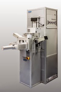
A cheap ellipsometer that can be integrated in ALD chambers for in-situ film growth monitoring from Film Sense. Thanks James Greer for posting this one in the ALD LinkedIn Group.
 
Innovative

By sampling discrete bands across the visible spectrum, the Film Sense FS‑1™ Banded Wavelength Ellipsometer realizes many of the benefits of spectroscopic ellipsometry without all the cost and complication.

Powerful

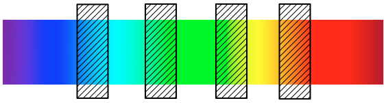
The film thickness and index of refraction of most transparent thin films can be determined with excellent precision and accuracy by a simple 1 second measurement. The multiple wavelength bands of the FS-1 enable the determination of additional sample parameters, such as multiple film thicknesses, surface roughness, and more.

Affordable

The FS‑1 offers the power of Banded Wavelength Ellipsometry™ (BWE), but at the price point of single wavelength ellipsometer and spectroscopic reflectometer systems. The FS‑1 is ideal for measurements in the research lab, classroom, in situ processing environments, industrial control, and more.

FS-1 Banded Wavelength Ellipsometer


FS-1 In Situ Monitoring Capabilities
  • Sub-monolayer thickness precision, in real time
  • Determine deposition rates and film optical constants n&k, at multiple process conditions, without breaking vacuum
  • Monitor and control the deposition of multilayer film structures
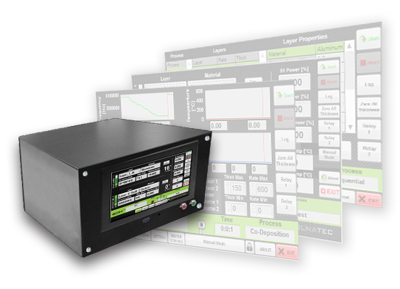
  • FS-API interface for external software control (LabVIEW™ compatible)
  • Applicable to most thin film deposition techniques: Sputtering, ALD, MBE, MOCVD, e‑beam evaporation, etc.

 
Mounting Specifications
  • Adapters for mounting the FS-1 light source and detector units to standard 2.75” or 1.33″ conflat vacuum flanges (windows not included)
  • Easy to adjust tilt stages for beam alignment
  • The FS-1 source and detector units are compact and light (≈1 kg each).
  • Can be installed without breaking chamber vacuum


Monday, November 17, 2014

SENTECH presents Real Time Monitor at ALD China Conference

SENTECH Instruments GmbH of Berlin, Germany, which manufactures equipment for plasma etching and deposition, atomic layer deposition (ALD) and thin-film measurements, has presented its new ALD Real Time Monitor in Asia at the 3rd China ALD Conference in Shanghai (16-17 October). 

For the first time the patented monitor allows the direct monitoring of absorption and desorption processes on the substrate surface during ALD processes within ALD half cycles.
 

Sentech PEALD system - The system can be equipped with several in-situ diagnostics tools e. g. QCM, QMS, ellipsometer. Ultra-fast in-situ ellipsometers are offered for monitoring layer-by-layer film growth applying laser ellipsometry as well as wide range spectroscopic ellipsometry


“Using the ALD Real Time Monitor enables efficient and fast process optimization,” says Dr Gargouri, SENTECH’s specialist for ALD processes, who gave a speech during the conference.


Wednesday, November 12, 2014

Colnatec Unveils All-Inclusive Thin Film Controller

Colnatec is expanding its portfolio of high-precision, thin film measurement and control devices, Colnatec today announced the debut of a compact controller that unites the leading-edge technology of its Eon™ series of PC-based controllers with the modular efficiency of rackmount instrumentation.


Thin Film Controller with Integrated Display
Adaptable. Affordable. Unconventional.


With its integrated display, intuitive user interface, and durable architecture, Eon-ID™ offers a versatile design that adapts easily to a variety of settings - ranging from industrial to laboratory to clean room to research environments - matching or surpassing the capabilities of Inficon™ XTC/3™ and IC6™.

“We’ve identified a growing demand for a stand-alone thin film control solution that incorporates hardware, display, and software into a single enclosure,” said Colnatec CTO Scott Grimshaw. “In answering this demand, Eon-ID™ has exceeded our expectations. Making thin film control more accessible through affordability and efficiency of design, Eon-ID™ has the potential of not only broadening thin film science in general but driving thin film manufacturing opportunities into completely new and unexpected areas of industry.”

Among its numerous features, Eon-ID™ offers the latest Eon Software™ interface, an integrated display allowing for a greater variety of settings and applications, rackmount capability, a temperature compensation system that maintains crystal to within +/- 1°C of preset temperatures, advanced technology that increases reliability and durability in industrial environments.

"Eon-ID™ employs the same temperature-centric technology used in our Eon™ and Eon-LT™ series controllers," noted Colnatec CEO Wendy Jameson. "Eon-ID™ will specifically benefit industries using atomic layer deposition (ALD), optics, OLED, and any other process that requires precision control over very thin layers, especially at temperatures higher than 100°C. Combining precision, simplicity, and cost effectiveness, Eon-ID™ represents nothing less than the state-of-the-art in thin film science."

About Colnatec

Taking a revolutionary approach to thin film design, development, and manufacturing, Colnatec (colnatec.com) manufactures the only commercially available heated quartz crystal microbalances (QCM) for process control of film thickness measurement in high temperature processes such as atomic layer deposition (ALD) or chemical vapor deposition (CVD). Through the use of patented and patent-pending Colnatec technology, researchers, manufacturers, and system-builders have reduced production and run times and costs to improve overall performance - ultimately achieving higher yields and improved process control. Colnatec technology is also frequently used in, encapsulation and high flux deposition of organic light emitting diodes (OLED), optical coatings such as for anti-reflection (PVD), next generation food packaging, and medical device coating, etc. Launched in 2009, Colnatec is the recipient of Department of Energy Phase I and Phase II SBIR awards for high temperature sensors, and one of eight winners of the inaugural Arizona Commerce Authority Innovation Challenge Grant. Colnatec has built a reputation as a bold innovator and a formidable player in a tough, highly competitive marketplace.

Wednesday, October 29, 2014

One ALD layer can increase the efficiency of photoelectrodes for water splitting

Here is a new paper from Massimo Tallarida and co-workers group in Cottbus at Brandenburg University of Technology in collaboration with Helsinki, Tartu and Alicante. The published paper below in Journal of Physical Chemistry Letters, gives for the first time a reasonable explanation of why 1 ALD layer can increase the efficiency of photoelectrodes for water splitting, just using the chemistry of ALD (in particular, only TMA).


Modification of Hematite Electronic Properties with Trimethyl Aluminum to Enhance the Efficiency of Photoelectrodes

Massimo Tallarida, Chittaranjan Das, Dejan Cibrev, Kaupo Kukli, Aile Tamm, Mikko Ritala, Teresa Lana-Villarreal, Roberto Gómez, Markku Leskelä, and Dieter Schmeisser

J. Phys. Chem. Lett., 2014, 5 (20), pp 3582–3587
 
 
The electronic properties of hematite were investigated by means of synchrotron radiation photoemission (SR-PES) and X-ray absorption spectroscopy (XAS). Hematite samples were exposed to trimethyl aluminum (TMA) pulses, a widely used Al-precursor for the atomic layer deposition (ALD) of Al2O3. SR-PES and XAS showed that the electronic properties of hematite were modified by the interaction with TMA. In particular, the hybridization of O 2p states with Fe 3d and Fe 4s4p changed upon TMA pulses due to electron inclusion as polarons. The change of hybridization correlates with an enhancement of the photocurrent density due to water oxidation for the hematite electrodes. Such an enhancement has been associated with an improvement in charge carrier transport. Our findings open new perspectives for the understanding and utilization of electrode modifications by very thin ALD films and show that the interactions between metal precursors and substrates seem to be important factors in defining their electronic and photoelectrocatalytic properties.
 
 
The building Panta Rhei, home for the Chair of Applied Physics and Sensors (Prof. Dr. Dieter Schmeißer) at Brandenburg Universitxy of Technology. The main research area of the department is spectroscopic and micro spectroscopic investigation of layers and layer structures in order to get information about the electronic properties and the geometrical structures of several materials, such as high-k oxides, metal and mixed oxides, inter metallic interfaces, semiconductors, conducting and semiconducting polymers, and with recent focus graphene. In addition, the department is very active in the research area of atomic layer deposition (ALD). In particular the initial layer growth is in the focus of interest. The layer deposition as well as the characterization are done in situ = "(in situ)2", where the characterization can be performed "cycle by cycle". (further information)

The authors conclude that the ALD of Al2O3 based on TMA produces modifications in the electronic properties of α-Fe2O3 favoring the improvement of its photoelectrochemical behavior. Reactions between TMA and α-Fe2O3 induce electron donation to the substrate in the form of small polarons and modify the covalent character of the Fe−O bonds. These Fe2O3 surface modifications probably allow for an enhanced charge carrier transport next to the interface and explain the photoelectrochemical enhancement observed in hematite photoanodes. We believe that this work contributes to the understanding of some of the mechanisms underlying the enhancement of hematite photoanodes by means of surface modification and that it may open new avenues for further improving their performance in the context of water splitting.


A vision of a sustainable hydrogen fuel community based on Artificial photosynthesis (APS) has been described in man yplaces and in particular in a relatively recent review in Nature Photonics (here).


Vision of a sustainable hydrogen fuel community based on Artificial photosynthesis (APS) - Hydrogen is produced from an APS solar water-splitting power plant using seawater on floating ports, tankers and seashore plants. Electricity needed to operate such an infrastructure is provided by renewable energy sources such as photovoltaic, wind and tidal power. (Nature Photonics, 6 (2012) 511)


Sunday, June 1, 2014

In situ characterization of ALD processes and study of reaction mechanisms for high-k metal oxide formation

"In situ characterization of ALD processes and study of reaction mechanisms for high-k metal oxide formation" is a fresh doctoral thesis to be defended 6th of June 2014 in Helsinki Finland by Mr Yoann Tomczak at University of Helsinki, Faculty of Science, Department of Chemistry, Laboratory of Inorganic Chemistry. To learn more on in-situ studies by QCM and QMS I recommend to read the doctoral thesis by Antti Rahtu that can be downloaded here.
 
Precursors, processes and materials studied in this thesis.
 
Yoann Tomczak
University of Helsinki, Faculty of Science, Department of Chemistry, Laboratory of Inorganic Chemistry
Doctoral dissertation (article-based), http://urn.fi/URN:ISBN:978-952-10-9926-7
 
Atomic Layer Deposition (ALD) is a thin film deposition method allowing the growth of highly conformal films with atomic level thickness and composition precision. For most of the ALD processes developed, the reaction mechanisms occurring at each step of the deposition remain unclear. Learning more about these reactions would help to control and optimize the existing growth processes and develop new ones more quickly. For that purpose, in situ methods such as quartz crystal microbalance (QCM) and quadrupole mass spectrometer (QMS) are used. These techniques present numerous advantages because they allow monitoring the thin film growth mechanisms directly during the process. Additionally, they do not require separate experiments or large amounts of precursors to test the efficiency of new processes and could be very effective means to monitor industrial processes in real time.

This thesis explores the most common in situ analytical methods used to study ALD processes. A review on the ALD metal precursors possessing ligands with nitrogen bonded to the metal center and their reactivity is provided. The results section reports the reaction mechanisms of ALD processes for the deposition of Nb2O5, Ta2O5, Li2SiO3, TiO2 and ZrO2. All the processes studied are using metal precursors with nitrogen bonded ligands and ozone or water for the deposition of high-k and other oxide films.
 
This is a Finnish article-based doctoral dissertation, the scientiffic work is mainly reported in the form of published or soon to be published journal articles:
 
I. “In situ reaction mechanism studies on the new tBuN=M(NEt2)3 -Water and tBuN=M(NEt2)3 - Ozone (M=Nb,Ta) Atomic Layer Deposition processes.” 
Y. Tomczak, K. Knapas, M. Sundberg, M. Ritala, M. Leskelä 
Chem. Mater.(2012), 24(9), 1555-1561 

II. “In situ reaction mechanism studies on atomic layer deposition of AlxSiyOz from Y. Tomczak, K. Knapas, S. Haukka, M. Kemell, M. Heikkilä, M. Ceccato, M. Leskelä, M. Ritalatrimethylaluminium, hexakis ethylaminodisilane and water.”
Chem. Mater.(2012), 24(20), 3859-3867
III. “In situ reaction mechanism studies on lithium hexadimethyldisilazide and ozone atomic layer deposition process for lithium silicate.”
Y. Tomczak, K. Knapas, M. Sundberg, M. Leskelä, M. Ritala
Journal of Physical Chemistry C (2013), 117(27), 14241-14246
 
IV. “In situ reaction mechanism studies on the Ti(NMe2)2(OiPr)2-D2O and Ti(OiPr)3(NiPr-Me-amd)-D2O Atomic Layer Deposition processes”
Y. Tomczak, K. Knapas, M. Ritala, M. Leskelä
Journal of Vacuum Science and Technology A: Vacuum, Surfaces, and Films (2014), 32(1), 01A121-01A121-7
V. “[Zr(NEtMe)2(guan-NEtMe)2] as a novel ALD precursor: ZrO2 film growth and mechanistic studies”
T. Blanquart, J. Niinistö, N. Aslam, M. Banerjee, Y. Tomczak, M. Gavagnin, V. Longo, E. Puukilainen, H.D. Wanzenböck, W.M.M. Kessels, A. Devi, S. Hoffmann-Eifert, M. Ritala, and M. Leskelä
Chem. Mater.(2013), 25(15), 3088-3095
 
VI. “Atomic layer deposition, characterization and growth mechanism of high quality TiO2 thin films”
VI. M. Kaipio, T. Blanquart, Y. Tomczak, J. Niinistö, M. Gavagnin, V. Longo, V. Pallem, C. Dussarrat, M. Ritala, M. Leskelä
submitted


How to build an ALD chamber for in situ x-ray diffraction

Stanford University present a ALD chamber for in-situ x-ray diffraction and scattering installed  at SLAC National Accelerator Laboratory, Stanford Synchrotron Radiation Lightsource. The  ALD chamber is designed for studying the structural properties of thin films during growth by high resolution XRD, GIXRD, and GISAXS. The ability to monitor the growth of an ALD material from nucleation to the formation of continuous films has been shown, and the precision to measure changes to the structure following single half-cycles has been demonstrated. According to the researchers, the design can also be adapted x-ray reflectivity (XRR) and x-ray absorption and fluorescence spectroscopy (XAFS). For all details please go ahead and access the all free content of the publication below.


The Stanford Synchrotron Radiation Lightsource (SSRL), a directorate of the SLAC National Accelerator Laboratory, is an Office of Science User Facility operated for the U.S. Department of Energy by Stanford University. SSRL provides synchrotron radiation, a name given to X-rays or light produced by electrons circulating in a storage ring at nearly the speed of light. These extremely bright X-rays can be used to investigate various forms of matter ranging from objects of atomic and molecular size to man-made materials with unusual properties. (news.slac.stanford.edu, Photo by Brad Plummer)

An atomic layer deposition chamber for in situ x-ray diffraction and scattering analysis
Scott M. Geyer, Rungthiwa Methaapanon, Richard W. Johnson, Woo-Hee Kim, Douglas G. Van Campen, Apurva Metha and Stacey F. Bent
Rev. Sci. Instrum. 85, 055116 (2014); http://dx.doi.org/10.1063/1.4876484

Abstract: The crystal structure of thin films grown by atomic layer deposition (ALD) will determine important performance properties such as conductivity, breakdown voltage, and catalytic activity. We report the design of an atomic layer deposition chamber for in situ x-ray analysis that can be used to monitor changes to the crystal structural during ALD. The application of the chamber is demonstrated for Pt ALD on amorphous SiO2 and SrTiO3 (001) using synchrotron-based high resolution x-ray diffraction, grazing incidence x-ray diffraction, and grazing incidence small angle scattering.


a) Cartoon depiction of the XRD chamber. (b) Depiction of the heater assembly with bridge mount and base plate. Citation: Rev. Sci. Instrum. 85, 055116 (2014); http://dx.doi.org/10.1063/1.4876484