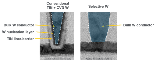
With continued scaling, however, contact dimensions have decreased to the point at which contact resistance is becoming a bottleneck in realizing optimum device performance. As the cross-sectional area of the contact shrinks, a growing proportion of the volume is occupied by metal liner/barrier and nucleation layers, leaving less volume for the conducting metal fill. In addition, multiple resistive interfaces in the plug contribute to higher contact resistance.
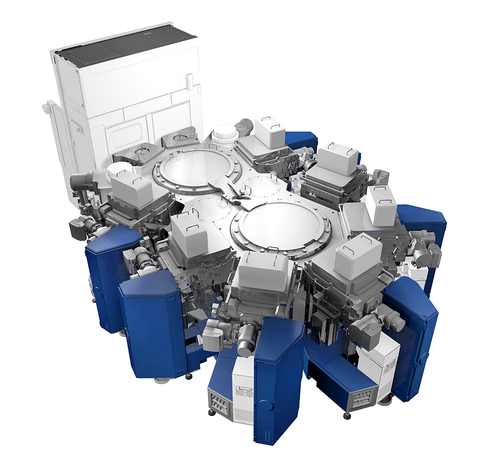
An Applied Materials Endura(TM) Platform equipped with seven Selective Tungsten CVD Volta(R) and 2 pre-clean 300 mm chambers. (Credit: Applied Materials)
The Applied Endura Volta Selective W CVD system offers an integrated materials solution that relieves these adverse effects with a breakthrough in 2D scaling. The system combines surface treatment chambers with selective tungsten deposition chambers. The selective deposition is enabled by both the unique process capabilities of the deposition chambers and the various surface treatments that use specialized chemistries to prepare the underlying metal and dielectrics of the contact to enable bottom-up, metal-on-metal deposition. The selective process eliminates both liner/barrier and nucleation layers to alleviate the bottleneck in device performance, and produces void- and seam-free gapfill.
Cross section of a leading edge Logic processor showing the Source/Drain contacts to the transistors and the metal interconnetcs (Credit: TechInsight, Applied Materials)
As all process steps are performed in an ultra-clean, continuous high-vacuum environment, the integrated materials solution ensures a pristine interface and defect-free contact fill. With the volume of conducting metal maximized, contact resistivity is substantially improved compared to conventional liner/barrier contact fabrication. This lower resistance facilitates higher device density and extends 2D scaling.
The selctive W CVD defect-free contact fill maximizes the volume of conducting metal (right), contact resistivity is substantially improved compared to conventional liner/barrier contact fabrication (left). (Credit: Applied Materials)


%20(1).png)


