Showing posts with label TSMC. Show all posts

Sunday, September 18, 2022

Samsung to focus on treatment of gas used in chip production to achieve net-zero emissions

A major cause of greenhouse gas emissions is process gas used in semiconductor wafer manufacturing comes from processing equipment such as reactive ion etching (RIE) and deposition (CVD and ALD). You can read and watch an interview here and study that paper that was recently published by me and my professor friends Henrik Pedersen and Sean Barry:


Green CVD-Toward a sustainable philosophy for thin film deposition by chemical vapor deposition

It is almost obvious that higher VPs at Samsung and TSMC (LINK) did just that ;-)

[Korea Herald, Link below] Advancing abatement technologies to reduce carbon emissions is the top priority in the Samsung Electronics semiconductor unit's goal to become carbon neutral by 2050, a top official said Friday.

"Treatment of gas used to manufacture semiconductor chips is our biggest focus in our spending (to achieve net-zero emissions)," Song Doo-guen, executive vice president and head of the Environment & Safety Center at Samsung Electronics, told reporters at a briefing in Seoul.


According to the article, Song Doo-guen, executive vice president and head of the Environment & Safety Center at Samsung Electronics, speaks at a briefing in Seoul, Friday and announced that:
  • Samsung has pledged a 7 trillion won ($5 billion) investment to achieve its climate ambitions, and announced that it had recently joined RE100, a coalition comprising 380 global enterprises committed to becoming 100 percent renewable.
  • Alongside the plan to cut direct carbon emissions, Samsung has also laid out a raft of plans to reduce indirect emissions, mainly by pursuing ultralow-power chip products.
  • Other eco-conscious plans it has drawn up include capping the maximum use of freshwater to 300,000 tons a day by 2030 and eradicating gaseous and liquid pollutants by 2040 with treatment technology.
Source: Samsung chip plants look to stamp out carbon footprint (koreaherald.com)

Inside TSMC, the Taiwanese chipmaking giant that’s building a new plant in Phoenix

[CNBC, link below] Recently CNBC got an exclusive tour of the US$ 12 billion semiconductor fab, in Phoenix, Arizona, where TSMC will start making 5 nm chips in 2024. The company says it will ramp up to produce 20,000 wafers each month.

“This project is designed as a 5 nm fab. Actually, it’s a copy from the fab we have in Taiwan,” Chen said.

Nearby, one of the world’s largest cranes was lifted to its full height of 200 feet. The 2,300-ton crane was brought to the site on 153 semi trucks. Site supervisor Jim White said contractors have moved nearly 4 million cubic yards of dirt and have used more than 260 million gallons of water since construction began in April.


Building a fab and making chips takes an incredible amount of water, not an abundant resource in the middle of the desert. Arizona’s biggest water source is groundwater, but deep wells at big farms are using water up faster than it’s naturally replenished. Chen said TSMC needs around 4.7 million gallons of water each day to support production. In Arizona, TSMC said, an on-site water treatment center will recycle up to 90% of water used at the fab.

Full article with video:

Thursday, September 15, 2022

TSMC to double energy efficiency and clean water consumption for semiconductor wafer manufacturing

According to TSMC 2021 Sustainability Report, they aim to by 2030, amongst many goals & actions:

  • double energy efficiency after five years of mass production for each process technology
  • reduce unit water consumption (liter/12-inch equivalent wafer mask layers) by 30% (Base year: 2010)
Link to report: e-all.pdf (tsmc.com)


Tuesday, August 30, 2022

Comparison confirms that SMIC reaches 7nm without access to western equipment & technologies

Similarities with TSMC 7nm have been found

After TechInsights revealed their initial findings on the SMIC MinerVa Bitcoin mining processor, their team did further analysis and comparison against TSMC 7nm. This new analysis confirms that despite current sanctions restricting access to the most advanced equipment technologies, Chinese Semiconductor Manufacturing International Corporation (SMIC) has used 7nm technology to manufacture the MinerVa Bitcoin Miner application-specific integrated circuit (ASIC).

The TechInsights analysis also uncovered many similarities between the SMIC 7nm and the TSMC 7nm, which are available in our comparison brief.


According to the SeekingAlpha assessment earlier this year (Applied Materials: SMIC Move To 7nm Node Capability Another Headwind (NASDAQ:AMAT) | Seeking Alpha) SMIC is using a large amount of multiple pattering mask layers like in the first TSMC and Samsung 7 nm nodes (N7). 

"At 7nm, normally 15 DUV systems and 5 EUV systems are demanded, depending on chip type and company. However, since SMIC is not permitted to use EUV, then they will be substituted by DUV, and 20 DUV systems will be used.

In both cases, multiple patterning is done to delineate that pattern, whether it is 28nm or 7nm. This multiple patterning process is more or less a trick to reach even the 28nm dimensions. The multiple patterning is typically a combination of deposition, etch, and lithography steps.

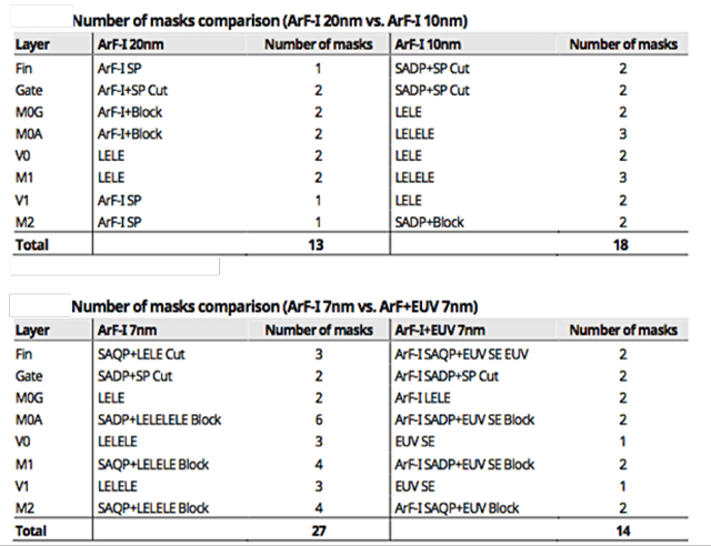
If we look at Chart 3 below, using immersion DUV (ArF-1) at the 20nm node there are 13 mask layers, each of which uses multiple dep-etch steps. If we move across the top of the chart, at 10nm there are 18 mask layers, an increase of 50% in the use of deposition-etch steps.

Multiple patterning at the 7nm node, as shown in the bottom left of the chart, requires 27 mask layers. However, by switching to EUV (bottom right) at 7nm, only 14 mask layers are required, similar to the 20nm node with DUV.

The terminology is as follows in switching from DUV to EUV:Double litho, double etch (LELE) process will be eliminated

While ArF-I would continue to be used for the self-aligned double patterning (SADP) and
Self-aligned quadruple patterning (SAQP) processes."
 

Table from SeekingAlpha as cited above

From an ALD point of view, the FEOL and metallization up to M2 use 19 in the case of Immersion Lithography (N7) vs 10 in the case of EUV (N7+) ALD spacer-defined multiple patterning masks (SADP or SAQP). However, the bigger difference is in etch for LELE etc., where EUV N7+ uses only 2 such masks.


Friday, January 7, 2022

TSMC Self-Aligned Via Process Development for Beyond the 3nm Node

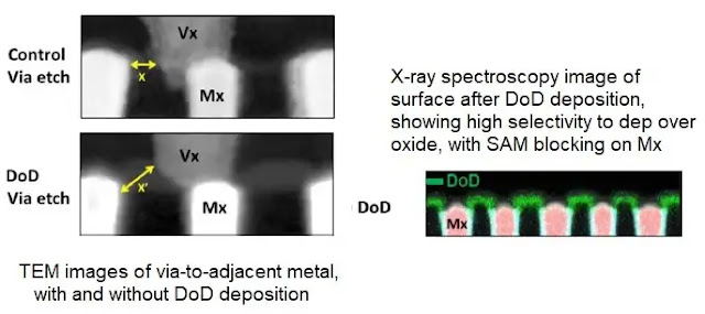
Semiwiki Tom Dillinger reports on an interesting paper by TSMC at the recent IEDM 2021 conference in San Francisco using selective ALD with the help of SAMs or Dielectric on Dielectric (DOD) as it is called.


From the article sumary: Continued interconnect scaling below the 3nm node will necessitate unique process development research to maintain electrical and reliability specs in the presence of (up to 4nm) overlay error. The need for low-K interlevel dielectrics is a given – yet, the via etch in these materials is not especially tolerant of EPE.

TSMC has demonstrated a potential process flow for a “self-aligned via” with an additional DoD material. The etch rate differential of the DoD results in more robust via-to-adjacent metal reliability. This process flow utilizes two unique steps – the SAM of a blocking material on metal surfaces, and the selective ALD of a dielectric-on-dielectric.

Tuesday, May 4, 2021

CBS 60 Minutes - Chip shortage highlights U.S. dependence on fragile supply chain

Seventy-five percent of semiconductors, or microchips — the tiny operating brains in just about every modern device — are manufactured in Asia. Lesley Stahl talks with leading-edge chip manufacturers, TSMC and Intel, about the global chip shortage and the future of the industry.
  • Pat Gelsinger: 25 years ago, the United States produced 37% of the world's semiconductor manufacturing in the U.S. Today, that number has declined to just 12%
  • Within the world of global collaboration, there's intense competition. Days after Intel announced spending $20 billion on two new fabs, TSMC announced it would spend $100 billion over three years on R&D, upgrades, and a new fab in Phoenix, Arizona, Intel's backyard, where the Taiwanese company will produce the chips Apple needs but the Americans can't make.

Intel CEO Pat Gelsinger shows CBS correspondent Lesley Stahl a silicon wafer.

Wednesday, March 24, 2021

Canon, SCREEN and Tokyo Electron to join Japan advanced chipmaking project for 2nm

Canon has partnered with Tokyo Electron and Screen Semiconductor Solutions to develop advanced chipmaking production technology with support from the Japanese government according to a report by Nikkei Asia.

♦ The $386mil USD funding from the Japanese government is through the National Institute of Advanced Industrial Science and Technology, along with the Ministry of Economy, Trade and Industry (METI).
♦ Japans semiconductor production industry has lost ground in recent years to Taiwanese chipmakers and companies like Intel.
The goal is to develop and implement a 2-nanometer or smaller process for chips by the mid-2020s.

Source (Paywall): LINK


Tokyo Electron semiconductor fab professionals shuffling wafers (credit: Tokyo Electron)

Saturday, February 27, 2021

2021 ISSCC - Plenary Session with Dr. Mark Liu, TSMC Chairman

TSMC recently delivered a plenary session at ISSCC 2021. by Dr. Mark Liu, TSMC Chairman. He gave a vision and path of how semiconductor technologies will continue to innovate over the coming years and decades. Below you can watch the Dr. Liu’s plenary session.

Abstract: The foundry business model, pioneered by TSMC more than three decades ago, brought a sea change to technology innovation and how integrated circuits (ICs) and systems are designed and manufactured. Access to semiconductor technology is no longer limited to large corporations that invest billions of dollars to build a fabrication plant. The foundry model has democratized IC innovation, making it available to all visionaries and innovators.

Today, an open innovation platform that connects innovators with semiconductor-technology providers is a vital link in the global supply chain. Our industry has already begun to look beyond just engineering individual chips manufactured on wafers, and have moved to integrate individual chips into systems. System performance and energy efficiency will continue to advance at historical rates, driven by innovations from many aspects, including materials, device and integration technology, circuit design, architecture, and systems. User applications drives design choices, and design choices are enabled by technology advancements. Advances in an open innovation ecosystem will further lower the entry barriers and unleash the future of innovation.


Saturday, November 28, 2020

Intel remains in the lead in 2020 semiconductor sales

IC Insights’ November shows the forecasted top-25 semiconductor suppliers in 2020. Seven top-15 semiconductor suppliers forecast to show ≥22% growth this year with Nvidia expected to post a huge 50% increase. The top-15 companies semiconductor sales are broken out into IC and O-S-D (optoelectronic, sensor, and discrete) device categories for 2019 and 2020. The forecasted 2020 top-15 semiconductor supplier ranking includes eight suppliers headquartered in the U.S., two each in South Korea, Taiwan, and Europe, and one in Japan.

Intel remains No 1. followed by Samsung and TSMC. 2020 show a very high growth for Fabless companies Qualcomm, Nvidia, MediaTek, Apple and AMD.

The Memory segment (DRAM and Flash) is led by SK Hynix +14% followed by Samsung +9% (incl. foundry) and Micron is down by -3%.

Please read the full IC Insights report here: LINK


Thursday, April 2, 2020

TSMC hit by 3nm delay fears over Covid-19 Lock-downs

TSMC is on schedule with its 5 nm process plan, but its 3 nm trial production may get delayed: The world's largest contract chipmaker is planning to launch mass production of its 3 nm process sometime in 2022, and media reported Monday that installation of production equipment in its 3 nm wafer fab in Tainan will be delayed to October from June this year, which will delay its trial production set for 2021. The COVID-19 escalation has hit Europe, and [Netherlands-based] ASML Holding, which is TSMC's major production equipment supplier, has been affected by a lockdown. It is understandable that the progress of TSMC's new technology has been affected.

Below a comparison of the Covid-19 daily new confirmed deaths, which is the only comparable parameter to use due to different testing capabilities and frequencies, in time and nation to nation. As can be seen the situation in Asian is under control after the gotten hit by the first wave of the Coronavirus. The European situation is stabilizing: Italy, Netherlands, Germany France, others look similar and are flattening the curve. In The USA situation is escalating. Many nations in Europe are forecasting a lift of Lockdown in May but are very careful, as an example Germany will decide in 19 April how to proceed according to Chancellor Dr. Angela Merkel.

BALD Engineering AB continues to monitor the Covid-19 situation due to lockdowns that affect the  the semiconductor industry – Stay Safe!

Google Finance (2020-04-02, 10:39 CET)

Sources:

Taiwan shares edge lower, TSMC hit by 3nm delay fears

Our World of data: https://ourworldindata.org/coronavirus

-----------
By Abhishekkumar Thakur, Jonas Sundqvist

Saturday, January 4, 2020

ASM International received TSMC’s Excellent Performance Award for ALD and Epitaxy products

ASM International N.V. (LINK) has received TSMC’s “Excellent Performance Award”, one of seven equipment suppliers to win this recognition in 2019. The award was presented to ASM by Mr. J.K. Wang, Senior Vice President Advanced Fab Operations, at the TSMC Supply Chain Management Forum on Dec 5, 2019, in Taiwan.

The award was received by ASM in recognition of its technology collaboration with TSMC. During the presentation, TSMC explained three points that contributed to the award to ASM. 

1) Outstanding development support.
2) Continuous efforts in productivity improvement.
3) Excellent delivery support on production ramp.

“On behalf of ASM and all of our employees, I thank TSMC for their recognition through this esteemed award,” said Chuck del Prado, CEO and President of ASM International. “Our partnership with TSMC is of strategic importance to ASM. We continuously focus on advancing our leading edge technology, including ALD and Epitaxy products and processes in support of our technology collaborations with TSMC."
 

ASM product portfolio for semiconducttor high volume manufacturing includes ewafer processing equipment for processes such as Atomic Layer Deposition (ALD), Plasma Enhanced ALD (PEALD), Epitaxy, Plasma Enhanced Chemical Vapor Deposition (PECVD), Low Pressure Chemical Vapor Deposition (LPCVD) and Oxidation/Diffusion. (source & credit www.asm.com)

Friday, June 28, 2019

TSMC has presented several research papers at the VLSI Symposium held in Japan.

TSMC has presented several research papers at the VLSI (Very-large Scale Integration) Symposium held in Japan

At the symposium, TSMC covered technologies ranging from pre-package soldering for eMRAM to a new chiplet design based on ARM’s Cortex A72 cores. TSMC also introduced a research paper on tungsten disulphide; a channel material that the fab believes will allow for improved electron flow at 3nm and beyond due to improved 2D electron switching. This tungsten disulphide short-channel transistor is manufactured through chemical vapor deposition directly on the silicon substrate, as opposed to earlier processes that required a sapphire intermediary. One research paper was titled ‘A 7nm 4GHz Arm®-core A72 based CoWoS® Chiplet Design for High-Performance Computing’.
Source: wccftech LINK
----------
By Abhishekkumar Thakur

Thursday, January 3, 2019

Innovation and IP filing in Atomic Layer Deposition has moved from Memory to Logic

By studying the filing of IP world wide one can clearly see the trend how innovation in Atomic Layer Deposition (ALD) has moved from Memory to Logic. During the introduction of ALD (2003 to 2006) in high volume manufacturing of DRAM on 300 mm wafers most IP was filed by Samsung, Micron and SK Hynix. 10 years later (2013-2018) the IP filing lead has been taken over by Logic MPU manufacturers TSMC, Intel and Globalfoundries.

The patent application assignee from the past 25 years.

ASM International received a supplier excellence award from TSMC

[ASM International, LINK] ASM International N.V. (Euronext Amsterdam: ASM) has received a supplier excellence award as one of five equipment suppliers from TSMC for the performance and support of ASM's CVD equipment and technology during 2018. The award was presented to ASM by Dr. C.C. Wei, TSMC's Chief Executive Officer, at the TSMC Supply Chain Management Forum on December 6, 2018 in Taiwan.

The award was received by ASM in recognition of its CVD technology and performance in production at TSMC fabs. During the presentation, TSMC explained three points that contributed to the award to ASM.

1) Close engagement with TSMC and precursor suppliers to innovate process solutions.

2) Continued effort on cost and productivity improvement.

3) Exceptional manpower arrangement for delivery.


"We are very honored to receive this prestigious award from TSMC. On behalf of ASM, I would like to thank TSMC for this recognition," said Chuck del Prado, CEO and President of ASM International. "ASM strives to continuously advance our technology solutions and our partnership with TSMC is of strategic importance to ASM. We are very pleased that TSMC has benefited from the performance of our ALD and Epitaxy deposition tools in its production fabs."

TSMC is the world's largest semiconductor manufacturing foundry. TSMC holds the Supply Chain Management Forum annually to show appreciation for the support and contributions of their suppliers and to recognize outstanding equipment and materials suppliers.

Friday, December 21, 2018

Chinese AMEC 5nm plasma etching tools verified by TSMC

DigiTimes report (LINK) that the Chinese OEM Advanced Micro-Fabrication Equipment (AMEC) announced recently its in-house developed 5nm plasma etching tools have been verified by Taiwan Semiconductor Manufacturing Company (TSMC). AMEC is already among TSMC's equipment suppliers for the foundry's 28nm, 10nm and 7nm processes.

Earlier in 2018 AMEC Introduced the Primo Nanova® System, which is the Company's first ICP etch Product for Chipmakers' most advanced memory and logic (LINK). Besides ICP AMEC has products based on CCP etch and platforms for TSV Etch (LINK).
 AMEC Introduced the Primo Nanova® System (AMEC)

Advanced Micro-Fabrication Equipment Inc. (AMEC)
AMEC is China's leading provider of advanced process technology to global manufacturers of semiconductors and solid-state lighting (SSL) products. Headquartered in Shanghai, the company is an entrenched supplier of dielectric and TSV Etch tools, helping chipmakers build devices at process nodes as low as 7nm. To date, nearly 800 AMEC process units have been positioned at 40 leading-edge semiconductor fabs across Asia. The company is also well established in Europe with AMEC MEMS tools running in production at major IDMs. In addition, with its MOCVD system, the company helps SSL manufacturers build today's most advanced LED products. To learn more about AMEC, please visit www.amec-inc.com.