Showing posts with label SiC. Show all posts

Wednesday, February 28, 2024

ASM International: Spearheading Semiconductor Innovation in ALD, Epitaxy, and CVD Markets

ASM International N.V. (Euronext Amsterdam: ASM) yesterday reported its fourth quarter 2023 operating results (unaudited). Double-digit full-year revenue growth, outperforming softer WFE market in 2023

“2023 was another successful year for ASM. Sales increased by 13% at constant currencies, despite softening market conditions, and marking the seventh consecutive year of double-digit growth.” said Benjamin Loh, CEO of ASM. “Revenue in Q4 2023 amounted to €633 million, in line with our guidance of €600-640 million and down compared to the level in Q4 2022. Revenue in the quarter was supported by strong sales in the power/analog/ wafer segment. Bookings at €678 million were slightly better than our expectation and were driven by GAA pilot- line orders and continued strength in China demand.

ASM's Leadership in the Growing ALD Market

According to ASM, the single wafer Atomic Layer Deposition (ALD) market is experiencing significant growth, with projections indicating an increase from $2.6 billion in 2022 to a range of $4.2 billion to $5.0 billion by 2027. This growth, characterized by a Compound Annual Growth Rate (CAGR) of 10-14% from 2022 to 2027, underscores the expanding role of ALD technology in semiconductor manufacturing. ASM International, a key player in the semiconductor industry, holds a dominant position in this market, commanding a share of over 55% throughout the forecast period.

Please note that this market assessment, most probably originally from TechInsights (prev. VLSI Research) does not include Large Batch furnace ALD, which historically have been about 30% of the total 300 mm ALD equipment market. The leaders in this segment are Tokyo Electron followed by Kokusai and ASM chose not to compete with its A412 ALD product line.

Driving Forces Behind ALD Market Expansion

The expansion of the ALD market is propelled by a series of technological advancements and increasing demands within the semiconductor sector. Key factors contributing to this growth include the industry's shift towards Gate-All-Around (GAA) technology, the necessity for advanced high-k gate dielectrics, and the precision required for threshold voltage tuning. Additionally, the development of sacrificial layers and the use of high aspect ratio Through-Silicon Vias (TSVs) are critical in advancing semiconductor manufacturing techniques. The application of metals and the adoption of selective ALD processes further accentuate the importance of ALD technology in modern semiconductor fabrication.


ASM's Strategic Positioning and Market Opportunities

ASM is well-positioned to capitalize on the opportunities presented by the burgeoning ALD market. The company's strategic emphasis on innovation, coupled with its comprehensive product portfolio, positions ASM as a frontrunner in meeting the evolving needs of the logic/foundry and memory segments of the semiconductor industry. The transition to advanced manufacturing technologies, such as GAA and high-k metal gate applications, presents significant growth avenues for ALD, with ASM at the forefront of this technological evolution.

To be more specific, the transition to GAA technology and the expansion in FinFET applications are set to significantly increase ASM's served available market by approximately US$400 million for every 100,000 wafer starts per month (WSPM). According to ASM, the equipment orders started to come in in the 2nd half of 2023. We can assume that this are orders from Samsung, TSMC and Intel. It is however about peculiar since Samsung had 3 nm GAA going already with yield in August 2023 and ASM is describing it as GAA pilot lines. Anyhow, come 2028 when all leading foundries including Rapidus in Japan are up and running GAAFETs, this additional market will be + USD 1.5 B as compared to if it would have been "only" FinFET technology - according to my back of the envelope calculations. For a company like ASM, with just below USD 3 B (2.6 B EUR) annual Revenue 2023 this is a huge thing. If this is not enough to go woah - add to that the GAAFET market is an upwards moving target and will continue to grow and looking ahead stacking of NMOS/PMOS will drive further demand for this type of ALD and Epi processes.

Expansion into the Epitaxy and CVD Markets

The Silicon Epitaxy (Si epi) market is also on a growth trajectory, with forecasts suggesting it will reach between $2.3 billion and $2.9 billion by 2027. ASM aims for a market share target of over 30%, focusing on both leading-edge and non-leading-edge segments. The leading-edge growth is driven by transitions to GAA technology and advancements in high-performance DRAM, while the non-leading-edge growth is buoyed by wafer power analog and strong momentum from ASM's Intrepid ESA. The epitaxy market is expected to see a Compound Annual Growth Rate (CAGR) of 3-8% from 2022 to 2027, with the leading-edge segment outpacing the overall market with a CAGR of 10-15%.

Regarding the SiC market, the investor presentation highlighted significant growth in power/analog/wafer revenue, almost doubling, primarily driven by robust demand in China. This growth was positively impacted by the consolidation of LPE (SiC Epitaxy), with sales comfortably exceeding the target of more than €130 million in 2023. This indicates ASM's strong performance in the SiC market and its successful integration and expansion in SiC epitaxy, aligning with the broader industry trend towards more advanced and efficient semiconductor materials.

Chemical Vapor Deposition (CVD) technology is another area of focus for ASM, particularly in the context of transitioning to new materials like Molybdenum, which is replacing traditional materials such as CVD Tungsten and PVD Copper in interconnect applications. This shift is indicative of the evolving needs within the semiconductor manufacturing process and highlights ASM's adaptability to changing market dynamics.

In summary, ASM's strategic initiatives in ALD, Epitaxy, and CVD technologies underscore the company's commitment to innovation and leadership within the semiconductor equipment market. Through a combination of market foresight, technological prowess, and strategic investments, ASM is well-positioned to capitalize on the growth opportunities presented by the evolving semiconductor landscape. 

Tuesday, February 6, 2024

Powering the Future: The Rise of Compound Semiconductor Substrates and Epiwafers

Yole Group reports that the compound semiconductor substrate market is on the brink of a significant transformation, poised to reach a staggering US$3.3 billion by 2029, with an impressive compound annual growth rate of 17% from 2023 to 2029. This growth is underpinned by the relentless innovation and strategic foresight of leading players like Wolfspeed and Coherent, who are continuously refining their product portfolios and expanding their market footprints.

Atomic Layer Deposition (ALD) and Atomic Layer Etching (ALE) play specific roles in the compound semiconductor industry. ALD is used to apply ultra-thin layers crucial for semiconductor devices, especially in insulating layers and gate dielectrics in transistors. ALE, with its precise etching capability, is key for crafting fine details in devices, often used in the patterning of nanoscale structures in LEDs and high-frequency transistors. These technologies support the development of advanced, reliable applications in power electronics and photonics.

At the heart of this industry evolution are the advancements in compound semiconductor technologies, spanning materials such as Silicon Carbide (SiC), Gallium Nitride (GaN), and Indium Phosphide (InP). These materials are catalyzing a revolution across various sectors, with SiC leading the charge in the automotive industry, particularly within the burgeoning 800V electric vehicle segment. GaN, on the other hand, is making inroads into consumer electronics and automotive applications, promising to redefine power electronics with its superior efficiency.

Check link below for High-Res graph

The impact of compound semiconductors extends beyond power electronics into the realm of photonics, where InP and GaAs are setting new benchmarks. InP, for instance, is witnessing a resurgence, driven by its critical role in AI applications, while GaAs photonics continues to grow, albeit at a steadier pace.

Yole Group, a market research and strategy consulting firm, in its latest "Status of Compound Semiconductors Industry 2024" report, provides an exhaustive analysis of these trends. The report delves into each substrate's market dynamics and technological advancements, offering a comprehensive overview of the ecosystem.

LINK: Compound semiconductors industry: an unprecedented promise (yolegroup.com)

As the industry stands at the precipice of transitioning to larger diameter substrates, the demand for high-data-rate lasers in AI is pushing for a shift to 6” InP substrates. Concurrently, GaAs is exploring the potential of 8” manufacturing for MicroLEDs, despite the challenges it faces against OLED technology.

In this dynamic landscape, companies like Wolfspeed and Coherent are not just participants but are leading the charge towards a more efficient, technologically advanced future. Their efforts in expanding material capacity and forging strategic alliances are testament to the industry's readiness to embrace the next wave of semiconductor innovation.


Friday, January 12, 2024

Onsemi Awards AIXTRON for Outstanding Contribution to SiC Fab Productivity in South Korea

Onsemi, a key player in the semiconductor industry, has recognized AIXTRON with a supplier award for its significant contribution to the rapid production ramp-up and productivity increase at onsemi's large silicon carbide (SiC) fabrication facility in South Korea. The facility, one of the world's largest SiC fabs, has benefited from the integration of AIXTRON's new G10-SiC systems. onsemi's successful collaboration with AIXTRON in tool installation and optimization led to substantial improvements in tool operations and maintenance, resulting in greater uptime and higher wafer output. The award from onsemi, a leading manufacturer in the semiconductor sector, highlights AIXTRON's service excellence and the impact of their technology in advancing onsemi's production capabilities.


Tuesday, September 19, 2023

Aixtron’s G10-SiC CVD System Supports GlobiTech’s SiC Epitaxy Expansion

  • GlobiTech Inc produces silicon carbide (SiC) and silicon epitaxial wafers, primarily focusing on serving the power and electric vehicle (EV) market segments.
  • GlobiTech Inc's production facilities are located in Sherman, Texas, USA.

Aixtron SE is aiding Texas-based silicon-epitaxy foundry GlobiTech Inc's entry into the silicon carbide (SiC) epitaxy market. The G10-SiC chemical vapor deposition (CVD) system from Aixtron has enabled GlobiTech to rapidly scale SiC epitaxy production in response to growing demand for power epiwafers. Featuring dual wafer sizes (9x150mm and 6x200mm), it offers high throughput per fab space. GlobiTech's expansion confirms the trend of SiC replacing silicon in various applications. Both firms have enjoyed a fruitful partnership, with Aixtron's tools maximizing wafer output. The G10-SiC is projected to be Aixtron's top-selling product in 2023.


Aixtron G10-SiC (Source Aixtron.com)

Source: AIXTRON Pressemeldungen :: AIXTRON

Recent Blog posts on SiC:

BALD Engineering - Born in Finland, Born to ALD: SiC Market Soars Towards $9 Billion: EVs and High-Power Chargers Drive Growth

BALD Engineering - Born in Finland, Born to ALD: SiC Market Soars Towards $9 Billion: EVs and High-Power Chargers Drive Growth

BALD Engineering - Born in Finland, Born to ALD: Samco launches new ICP Tornado Plasma ALD system

BALD Engineering - Born in Finland, Born to ALD: ASM International has completed the acquisition of Italian Silicon Carbide Equipment Manufacturer LPE S.p.A.

BALD Engineering - Born in Finland, Born to ALD: Chemistry paves the way for improved electronic materials - LiU have developed a new molecule that can be used to create high-quality indium nitride

Background:

  • Silicon carbide: from gold rush to commodity?1, which provides an overview of the global SiC market and its predictions for the future of the technology. It discusses the growth rate, size, and drivers of the SiC device market, as well as the competitive landscape and supply chain of the SiC industry. It also analyzes the challenges and opportunities for SiC technology in different applications, such as automotive, industrial, energy, and telecommunications. It also compares and evaluates SiC with other wide bandgap materials, such as gallium nitride (GaN) and diamond.
  • The 2023 global fab landscape: opportunities and obstacles2, which considers the state of the global semiconductor fab market in a post-COVID world. It discusses the emerging business models that could enable the semiconductor industry to migrate to leading-edge and mature technology with optimal manufacturing capacity. It also examines the impact of COVID-19, trade wars, and geopolitical tensions on the semiconductor supply chain and fab investments. It also explores the trends and innovations in semiconductor materials, devices, and modules, such as silicon carbide (SiC), gallium nitride (GaN), and quantum computing.


Friday, September 1, 2023

SiC Market Soars Towards $9 Billion: EVs and High-Power Chargers Drive Growth

Strategic Shift to 8-Inch Wafers: Opportunities and Challenges Shape SiC's Next Phase

According to Yole, the Silicon Carbide (SiC) market is on a robust trajectory, poised to reach nearly $9 billion by 2028, driven by a dynamic blend of growth factors. The automotive sector, particularly Battery Electric Vehicles (BEVs) and 800V EV systems, spearheads this expansion. SiC's prominence extends to EV DC chargers, offering immense potential for high-power modular chargers. Additionally, SiC plays a pivotal role in energy supply, with installations expected to surge between 2022 and 2028. Industrial power supplies, motor drives, and rail systems further diversify SiC's applications. This Yole report underscores SiC's prowess in high-efficiency power electronics across industries, shaping a transformative market landscape.

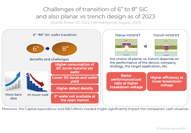
The report indicates that as of 2023, the mainstream SiC wafer size for leading players is still 6 inches. However, there are strategic discussions and plans surrounding the transition to 8-inch (200 mm) SiC wafers. While Wolfspeed is currently the only player producing SiC devices on the 8-inch platform, other companies have announced their intention to follow suit. The adoption of 8-inch wafers presents both opportunities and challenges.


Challenges associated with 8-inch wafer production include higher costs, longer equipment lead times, potentially lower initial yield rates due to the larger size, and concerns about the availability of these wafers. Wolfspeed's early adoption of 8-inch wafer production reflects their proactive stance in developing the technologies and processes required to overcome these challenges.


The transition to 8-inch wafers is an area of focus due to the potential advantages it offers, such as increased capacity and improved cost efficiency over time. However, the challenges mentioned earlier are critical factors that need to be addressed for a successful transition. Companies are investing in innovative approaches and strategies to ensure a smooth migration to the 8-inch platform, which has the potential to impact the SiC power devices market significantly in the coming years.

Yole Group - Follow the latest trend news in the Semiconductor Industry

Tuesday, October 4, 2022

ASM International has completed the acquisition of Italian Silicon Carbide Equipment Manufacturer LPE S.p.A.

ASM International (Euronext Amsterdam: ASM) today announces that it has completed the acquisition of LPE S.p.A., after having received regulatory approvals.

On July 18, 2022, ASM entered into a definitive agreement under which it would at closing acquire all of the outstanding shares of LPE, an Italian based manufacturer of epitaxial reactors for silicon carbide (SiC) and silicon. As announced in our press release of July 18, 2022, the transaction is financed with a combination of cash, a conditional earn out, and 631,154 ASM shares (a combination of 580,000 treasury shares and 51,154 newly issued shares).


The acquisition has been completed today, and LPE is now a fully owned subsidiary and will operate as a product unit under ASM’s Global Products organization.

“This is an important milestone for ASM. We are excited to welcome LPE and its talented and experienced team into ASM,” said Benjamin Loh, President and CEO of ASM. “Together with LPE we look forward to capturing many of the opportunities in the high-growth silicon carbide epitaxy market and to support our power electronics customers with innovative solutions, driving the further electrification of the automotive industry.”
“I believe ASM is the right partner for LPE, especially now looking at the growth we are seeing in the silicon carbide market. The global reach that ASM has with its entrenched supplier and customer networks will bring benefits to all stakeholders,” said Franco Preti, who envisioned the silicon carbide opportunity in the earliest stages and led LPE growth as CEO until the acquisition.

LPE is profitable with margins in line with ASM’s 2021-2025 target model. As announced earlier, LPE’s revenue is projected to grow to more than €100 million in 2023, mainly driven by its SiC epitaxy equipment business. Based on ASM internal estimates, demand for SiC epitaxy equipment is forecasted to grow at a CAGR in excess of 25% from 2021 to 2025, driven by the rapidly expanding market for electric vehicles.

Wednesday, November 18, 2020

Japanese researchers enable high thru put conformal CVD for SiC on Silicon wafer integration

As reported by ACS (LINK) New, concise method proposed for conformal chemical vapor deposition using sacrificial layers (SLs). SLs are porous membranes that filter high sticking-probability species, while allow the passage of low ones.

This is a really clever by researchers at University of Tokyo and IHI Corporation for CVD to compete with ALD on conformality and keeping a high deposition rate and at the same time produce bulk material like SiC on Si for larger wafer diameter.


Figure from ACS Twitter post (LINK)

Reference:

Porous Membranes as Sacrificial Layers Enabling Conformal Chemical Vapor Deposition Involving Multiple Film-Forming Species
Kohei Shima, Yuichi Funato, Noboru Sato, Yasuyuki Fukushima, Takeshi Momose, and Yukihiro Shimogaki
ACS Appl. Mater. Interfaces 2020, 12, 45, 51016–51025
Publication Date:October 30, 2020
https://doi.org/10.1021/acsami.0c14069