


%20(1).png)
Silicon photonics technology is fast becoming the linchpin in the quest to meet the soaring demands for data center bandwidth, with a particular focus on its application in artificial intelligence (AI) and machine learning (ML). This transformative technology leverages the power of photons to create efficient interconnections within data centers, a development recognized by experts at imec, a leading semiconductor research lab, as increasingly crucial.
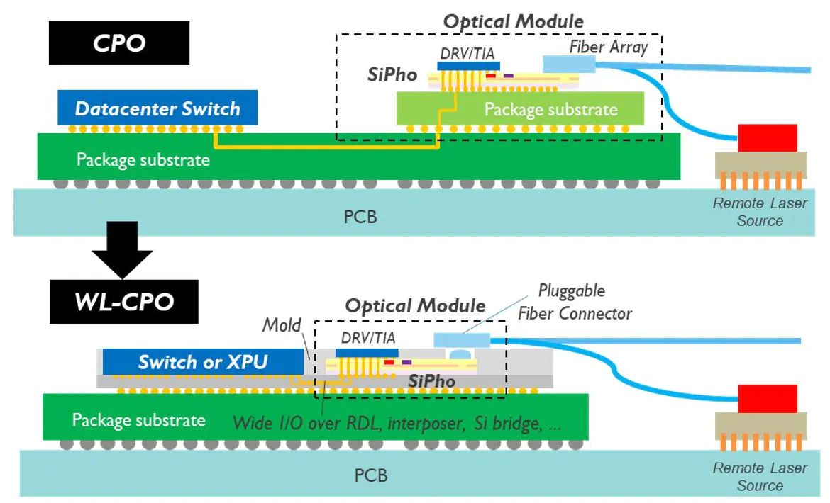
In the imminent future, silicon photonics is set to revolutionize chip-to-chip connectivity among central processing units (CPUs), graphics processing units (GPUs), and other core computational elements at the heart of data centers and AI supercomputers. Despite formidable challenges in tightly integrating optics and electronics, the semiconductor industry is rising to the occasion, epitomized by the development of switch chips featuring co-packaged optics. imec envisions substantial enhancements in the power efficiency, bandwidth density, and cost-effectiveness of silicon photonics, potentially paving the way for advanced co-packaged optics, such as "wafer-level optical interconnects," capable of achieving near-light-speed data transfer between chips on printed circuit boards (PCBs) or within packages.
Source: Silicon Photonics Will Shine in the Age of AI | Electronic Design
In summary, silicon photonics stands as a pivotal solution to address the burgeoning bandwidth requirements of data centers, with a particularly promising role in the realm of AI and ML applications. imec's concerted efforts in advancing this technology promise to shape the future of high-speed optical interconnect networks, ushering in an era of unprecedented computational capabilities.
