Showing posts with label MOCVD. Show all posts

Saturday, January 13, 2018

MPD Chemicals Acquires Specialty Chemical Manufacturer Norquay Technology

Norqay Technology, a company with more that 30 years experience in organo metallic precursors for ALD and CVD has just been acquired by MPD Chemicals. Please find press release below.

TREVOSE, Pa., Jan. 11, 2018 /PRNewswire/MPD Chemicals (MPD), a US-based manufacturer of specialty chemicals and custom synthesis solutions, announced today the expansion of its manufacturing capabilities, product portfolio and customer base with the acquisition of Norquay Technology, Inc. (Norquay). Located in Chester Pennsylvania, Norquay is the fourth acquisition to be integrated into the MPD Holdings platform, an Addison Capital portfolio company; existing MPD businesses include Monomer Polymer & Dajac Labs, Silar, and IsoSciences.

Norquay is a specialty chemical manufacturer with over 30 years of expertise in providing the scale-up and production of advanced proprietary custom materials, including organometallic, inorganic and organic molecules. Norquay’s product line includes chromic, electronic, catalyst, ligand, medical adhesive and UV performance products, with a customer base that ranges from startups to large multi-national corporations.

Wednesday, January 10, 2018

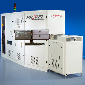
Osram orders multi-reactor Propel HVM and K475i MOCVD systems from Veeco for high-volume photonics and LED applications

Epitaxial deposition and process equipment maker Veeco Instruments Inc of Plainview, NY, USA says that Osram Opto Semiconductors GmbH of Regensburg, Germany has ordered a multi-reactor Propel High-Volume Manufacturing (HVM) gallium nitride (GaN) metal-organic chemical vapor deposition (MOCVD) system, as well as K475i MOCVD systems. 

The K475i system incorporates Veeco’s Uniform FlowFlange technology, producing films with very high uniformity and improved within-wafer and wafer-to-wafer repeatability with what is claimed to be the industry’s lowest particle generation for demanding applications like photonics and advanced LEDs.  

Source: Semiconductor Today LINK


Incorporating proprietary TurboDisc and Uniform FlowFlange™ MOCVD technologies, the new K475i system enables Veeco customers to reduce LED cost per wafer by up to 20 percent compared to alternative systems through higher productivity, best-in-class yields and reduced operating expenses. (Source: Veeco LINK)

Wednesday, September 27, 2017

AIXTRON provides novel deposition system to EPFL for 2D materials research

Leading Swiss university focuses on the development of next-generation semiconductors based on AIXTRON BM system

 
AIXTRON SE (FSE: AIXA), a worldwide leading provider of deposition equipment to the semiconductor industry, today announced that the École Polytechnique Fédérale de Lausanne (EPFL) in Lausanne (Switzerland) has purchased a BM NOVO system. This versatile tool which can produce virtually all variations of 2-dimensional materials (2D) required for emerging optoelectronic applications is dedicated to support the University’s research projects coordinated by Prof. Andras Kis and Prof. Aleksandra Radenovic.

AIXTRON’s BM NOVO system uses a unique combination of plasma-enhanced chemical vapor deposition (PECVD) technology and metal organic chemical vapor deposition (MOCVD) technology to enable the growth of high quality 2D materials such as transition metal dichalcogenides (TMDCs) e.g. molybdenum disulfide (MoS2) or tungsten diselenide (WSe2).

Source: Aixtron LINK

Thursday, September 21, 2017

Swedish-American glō Orders G5+ MOCVD System for Micro-LED Production

This summer Google announced that it has invested 15 million USD for a 13 percent stake in Glo, a Swedish Lund University spin-out focused on creating nanowire-based LED-displays for mobile phones and smart watches as well as AR- and VR-applications (LINK). 

Now Aixtron Reports: AIXTRON SE (FSE: AIXA), a worldwide leading provider of deposition equipment to the semiconductor industry, announced today that it has received an order for an AIX G5+ platform from Swedish-American company glō-USA, Inc. The group focuses on the commercialization of micro-LED (mLED) products based on their proprietary defect-free GaN nanowires technology. Such 3D structures enable the growth of mLEDs while maintaining the reliability of an inorganic material system. AIXTRON’s AIX G5+ Planetary Reactor® system was selected in the scope of glō’s strategic expansion and will be delivered with an 8x150 mm configuration in the course of Q4/2017.

Sunday, August 20, 2017

Atomic layer etching of MOCVD epitaxial gallium nitride

As have been reported before by Lund Nano Lab in Sweden (e.g. at ALE2016 Ireland and ALE2017 Denver) it is quite possible to use a standard ICP reactive ion etch chamber to run Atomic Layer Etching (ALE). Here is a nice publication from Aalto University in Finland and current and ex scientists from Lund Nano Lab in Sweden transferring the ALE processes from Lund and running it on an Oxford Instruments Plasmalab 100 in ALE mode etching GaN in Helsinki Micronova clean room.


The Oxford Instruments Plasmalab 100 at Aalto University Micronova clean room (LINK to technical specs and capabilities) 

MOCVD grown epitaxial AlGaN/GaN heterostructures implemented in high electron mobility transistors (HEMTs) have a well-defined layered structure with the two-dimensional electron gas (2DEG). However, etching of the gate recess is challenging as conventional RIE does not provide sufficiently good control over the etch process, and high energy ions can cause damage to the 2DEG layer. This paper showcase how these problems can be avoided if GaN ALE is used in etching these recesses.


Sabbir Khan - the ALE King tuning the Plasma at Lund Nano Lab.

Besides techniques of growing a single monolayer or few monolayers of GaN are challenging. GaN ALE could provide an alternative method to the 2D material community by a controlled thinning of high quality films of GaN down to a few atomic layers.

Please find the abstract to the Open Access JVSTA publication below:


Atomic layer etching of gallium nitride (0001)
Christoffer Kauppinen, Sabbir Ahmed Khan, Jonas Sundqvist, Dmitry B. Suyatin, Sami Suihkonen, Esko I. Kauppinen, and Markku Sopanen

Journal of Vacuum Science & Technology A: Vacuum, Surfaces, and Films 35, 060603 (2017); doi: http://dx.doi.org/10.1116/1.4993996


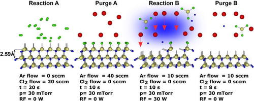
Abstract: In this work, atomic layer etching (ALE) of thin film Ga-polar GaN(0001) is reported in detail using sequential surface modification by Cl2 adsorption and removal of the modified surface layer by low energy Ar plasma exposure in a standard reactive ion etching system. The feasibility and reproducibility of the process are demonstrated by patterning GaN(0001) films by the ALE process using photoresist as an etch mask. The demonstrated ALE is deemed to be useful for the fabrication of nanoscale structures and high electron mobility transistors and expected to be adoptable for ALE of other materials.

Saturday, August 19, 2017

OSRAM Opto Semiconductor Acquires MOCVD Systems from AIXTRON

AIXTRON announced that OSRAM Opto Semiconductors has purchased the company's AIX 2800G4-TM Planetary system for the manufacturing of mainly infrared-based high power lasers and LEDs based on gallium arsenide (GaAs).

Source: LEDinside LINK
Photo credit: Aixtron (www.aixtron.com)
From Aixtron Press release: “We are very pleased that OSRAM Opto Semiconductors has selected our AIX 2800G4-TM platform for the production of high power laser and infrared LED devices. Their trust in our AIX 2800G4-TM system confirms our strategy to focus on solutions for the most demanding applications, where superior process performance is mandatory to meet our customer’s requirements. Following the recent qualification of our AIX G5 C platform and achieving this key milestone also with the AIX 2800G4-TM, we are looking forward to further deepen our partnership with one of the most innovative semiconductor manufacturers worldwide”, explains Dr. Frank Schulte, Vice President AIXTRON Europe.

Friday, December 2, 2016

President Obama set to block Aixtron sale

Seeking Alpha reports that President Obama is poised to block a Chinese company from buying Germany's Aixtron (NASDAQ:AIXG) because Northrop Grumman (NYSE:NOC), a major U.S. defense contractor, is among the chip equipment maker's customers.

It would mark only the third time in more than a quarter century that the White House rejected an investment by an overseas buyer as a national security risk.

Aixtron shares -6.5% in Frankfurt.


China Warns U.S. Against Blocking Aixtron Takeover

Aixtron shares fall amid U.S. national security concerns over acquisition by China’s Fujian Grand Chip Investment Fund [Wall Street Journal]

Obama bars China's Fujian from buying Aixtron's US business


The headquarters of German chip equipment maker Aixtron SE is pictured ... The Treasury Department said Obama was blocking the deal .. [Reuters]

Warum redet Amerika in der Aixtron-Übernahme mit?

Die Übernahme des deutschen Maschinenbauers Aixtron durch einen chinesischen Investor ruft die große Politik in Washi [FAZ - Frankfurter Allgemeine Zeitung]

Tuesday, May 24, 2016

China to enter Leading Edge ALD Market by Aixtron take over

Most focus on the reporting for the current Aixtron situation is typically focusing on MOCVD and LED business. However, I find it naturally much more interesesting in the sense of China taking over the ex-Genus ALD business unit based in Sunnyvale (USA). Aixtron is currently on the ALD Top 10 OEM ranking for ALD (Number 7 possibly) and this is a booming market because of multi patterning coming strong now and in the following nodes. Aixtron has a multi wafer ALD plattform that can most probably be used for multi patterning as well so this to me much more interesting potential than their LED business. In addition, Aixtron has had recent success on the Korean DRAM market. So just imagine the new situation if the next grand chip investment will be an etch company.


AIXTRON SE (FSE: AIXA; NASDAQ: AIXG) (“AIXTRON”) and Grand Chip Investment GmbH (“Grand Chip Investment”), a 100% indirect subsidiary of Fujian Grand Chip Investment Fund LP (“FGC”), have today entered into an agreement to take over AIXTRON. Fujian Grand Chip Investment Fund LP is a Chinese investment fund; 51% of which is held by the Chinese business man Zhendong Liu and 49% by Xiamen Bohao Investment Ltd.

Pursuant to the agreement, Grand Chip Investment has today announced its decision to launch a voluntary public takeover offer to acquire all of the outstanding ordinary shares of AIXTRON SE, including all ordinary shares represented by AIXTRON ADS. Under the terms of the agreement, AIXTRON shareholders will be offered 6.00 Euros in cash per each ordinary share. The transaction values AIXTRON’s equity, including net cash, at approximately 670 million Euros and reflects a 50.7% premium to the three-month volume weighted average share price prior to announcement. The offer shall be subject to certain closing conditions, including regulatory approvals and a minimum acceptance threshold of 60% of all of AIXTRON’s outstanding shares.

The agreement sets out the purpose and the principal terms of the transaction with FGC and the future strategy. FGC intends to support AIXTRON’s strategy going forward. R&D competency and AIXTRON’s existing technology shall be maintained at the existing technology centers. FGC has also agreed that AIXTRON shall further strengthen its technology and IP Portfolio, which shall remain vested with AIXTRON, including in Germany. AIXTRON’s existing global set up will be maintained and expanded with AIXTRON’s three technology hubs in Herzogenrath (Germany), Cambridge (UK) and Sunnyvale (USA). Further international technology hubs may be established. AIXTRON’s legal domicile and headquarters shall remain in Herzogenrath, Germany.

In the event the takeover is successful, Martin Goetzeler is to remain CEO of AIXTRON and Dr. Bernd Schulte is to remain in his function as COO. Following a successful closing of the transaction it is anticipated that Grand Chip Investment will nominate four candidates to the six-member Supervisory Board.

Monday, April 4, 2016

New Critical Materials Conference's Powerful Agenda


 Buy Reports  | CMC Fabs   |  CMC Conference  |  Register Now
New Critical Materials Conference's Powerful Agenda
May 5-6, Hillsboro Oregon
The Critical Materials Conference provides a framework to catalyze the flow of "actionable" technical and supply chain information related to critical materials. 

New Additions to the Critical Materials Conference Include: 
  • David Thompson, Ph.D., Director of Process Chemistry of Applied Materials
    • Agony in New Material Introductions - Minimizing and Correlating Variabilities
  • Suresh Ramalingam, Sr. Director, Advanced Packaging Development of Xilinx
    • Packaging Materials - Future Challenges 
A highly differentiated program, with networking opportunities for all attendees. 
For full agenda details click here.

Themes of the Conference are centered around the needs of the Critical Materials Council and the global IC fabrication industry. While executive conferences typically focus on the "what" and "why" of materials technologies, this conference will discuss "how" new materials can be controllably, safely, and cost-effectively used in fabs. The Conference will also include market data to validate "when" materials will be needed. Attendees from fabs, OEMs, and materials suppliers alike will have the opportunity to interact with the presenters and colleagues, to gain insights into best-practices of the entire supply-chain.
 
For more information on the conference go to www.cmcfabs.org/seminars/ 
Great Sponsorship Opportunities available, 
please contact cmcinfo@techcet.com or call 1-480-382-8336

Sponsors and Committee

Wednesday, March 23, 2016

Aixtron soars after qualification with Taiwanese Epistar LED chipmaker

Press release from Aixtron:
AIXTRON SE (FSE: AIXA; NASDAQ: AIXG), a worldwide leading provider of deposition equipment to the semiconductor industry, announced today that Epistar Corporation, a global leading supplier of LED chip products, has successfully achieved all milestones in the internal qualification process of the AIX R6 beta-type MOCVD production system (“AIX R6” hereafter). 


In the course of the qualification process, the AIX R6 confirmed its value proposition in terms of throughput maximization, intrinsic yield and uniformity. Particularly designed for LED mass production, the AIX R6 also demonstrated its cost advantages through precursor efficiency and continuous run production modus. 

“We have been satisfied with the performance of AIXTRON’s Showerhead tool during the internal test phase, especially with its improved uniformity which is the basis for high-quality LED products. We are looking forward to benefit from the system’s low cost of ownership in the future”, says Dr. M. J. Jou, President of Epistar Corporation. 

“The AIX R6 is a state-of-the-art LED manufacturing system that recognizes the needs of the LED industry, especially with regard to output, efficiency and costs. Based on our longstanding and trustful business relationship with Epistar, we are looking forward to the further cooperation with one of the leading and most innovative players in the global LED market”, comments Dr. Bernd Schulte, Executive Vice President and COO of AIXTRON SE.“ 

Located at the Hsinchu Science-based Industrial Park, Taiwan, Epistar Corporation has been driving the development, manufacture and marketing of ultra-high brightness (UHB) LED products for over a decade. Via its proprietary MOCVD process technology, Epistar continues to successfully commercialize worldwide a full range of UHB LEDs having compact size, low power consumption and long operation life.

Saturday, March 12, 2016

LG Innotek teams up with AIXTRON technology


According to a recent press release (see below) LG Innotek teams up with AIXTRON technology. The Korean electronic components specialist counts on AIX G5 WW system for the developmnt of silicon carbide epitaxial wafers 


AIXTRON SE (FSE: AIXA; NASDAQ: AIXG), a worldwide leading provider of deposition equipment to the semiconductor industry, announced today that one of Korea’s leading electronics companies, LG Innotek has selected a AIX G5 WW (Warm-Wall) reactor for the development of silicon carbide (SiC) epitaxial wafers aimed mainly at power devices for automotive and renewable energy applications. The system configured for 8x6-inch substrates was delivered in the fourth quarter 2015.  


Thursday, February 18, 2016

Veeco Instruments, imec Enter Development Deal for Gallium Nitride Epi Wafers

Veeco Instruments reported that it has signed a joint development project (JDP) agreement with imec, a Belgium-based nano-electronics research center, to accelerate the development of Gallium Nitride (GaN) based, power electronic devices using GaN Epi wafers. Under the development project, the GaN Epi wafers will be created using Veeco’s Propel Power GaN metal organic chemical vapor deposition (MOCVD) system. Veeco’s Propel® Power GaN MOCVD system.


Veeco’s Propel™ Power GaN MOCVD system is designed specifically for the power electronics industry. Featuring a single-wafer reactor platform, capable of processing six- and eight-inch wafers, the system deposits high-quality GaN films for the production of highly efficient power electronic devices. The single-wafer reactor is based on Veeco’s leading TurboDisc® design with breakthrough technology, including the new IsoFlange™ and SymmHeat™ technologies that provide homogeneous laminar flow and uniform temperature profile across the entire wafer. Customers can easily transfer processes from Veeco K465i™ and MaxBright™ systems to the Propel Power GaN MOCVD platform. (www.veeco.com)

Imec has already demonstrated significant gains in GaN layer uniformity and run-to-run repeatability with Veeco’s Propel system, resulting in significantly improved power device yields. The single wafer reactor incorporates Veeco’s proprietary TurboDisc® technology that delivers superior film uniformity, run-to-run control and defect levels compared to batch reactors.

Monday, February 1, 2016

Epiluvac and SAMCO to offer processing equipment for WBG materials in Nordic countries

As earlier reported here on the BALD Blog Epiluvac from Sweden and SAMCO from Japan has signed a collaboration deal. Now the to partners have signed an extened agreement to include distribution of SAMCO products in Scandinavia. Interestingly SAMCO also have an ALD product line. See also previous report on ALD here.


 Epiluvac’s EPI-1000X silicon carbide reactor.


SAMCO's new AL-1 ALD system.
 
As reported by Solid State Technology : Sweden-based SiC CVD developer and manufacturer Epiluvac AB has entered into a collaboration with SAMCO, a semiconductor process equipment developer and manufacturer based in Japan, in which Epiluvac will introduce new clients to SAMCO in Sweden, Norway, Finland and Denmark.


Bo Hammarlund, Chair , CEO, founder  of Epiluvac AB
 
SAMCO offers systems and services that revolve around three major technologies: 1) thin film deposition with PECVD, MOCVD and ALD systems, 2) microfabrication with ICP etching, RIE and DRIE systems, and 3) surface treatment with plasma cleaning and UV ozone cleaning systems.

“With this collaboration, Epiluvac and SAMCO are both acting as a one-stop solution,” says Bo Hammarlund, managing director of Epiluvac AB. “We offer our expertise to help customers decide upon the best combinations in terms of processing equipment for WBG materials, including both SiC and GaN materials.”

Tuesday, November 17, 2015

CVD Equipment Corporation Revenue Rose 20.1% to Record-breaking Levels

It is soon Christmas so I think we ALD guys can be nice to the CVD guys. Some brief news from the world of CVD: CVD Equipment Corporation announced that it has achieved record-breaking revenue for both the three and nine month periods ended September 30, 2015. CVD’s revenue rose 20.1% to a record-breaking level of $10.6 million for the current quarter ending September 30, 2015 compared to $8.9 million in revenue for the quarter ended September 30, 2014. For the current nine month period, CVD’s revenue rose 59.0% to a record-breaking $30.8 million compared to $19.4 million in revenue for the nine month period ended September 30, 2014.  CVD also reported net earnings of $0.8 million or $0.13 per basic and diluted share and $2.8 million or $0.46 per share basic and $0.45 per share diluted for those respective periods compared to earnings of $0.9 million or $0.14 per share basic and diluted and $0.8 million or $0.13 per share basic and diluted for the three and nine months ended September 30, 2014


Full report: http://www.cvdequipment.com/2015/11/16/cvd-revenue-rose-20-1-to-record-breaking-levels/

Joiking aside,  CVD Equipment Corporation actually have an ALD Product offering. I do not know too much about this and here is the generic information that is available through their web:

Atomic layer deposition (ALD) is a thin film deposition process that allows for atomic layer thickness resolution, excellent conformity of high aspect ratio surfaces, and pinhole-free layers. This is achieved by sequential formation of atomic layers in a self-limiting reaction.


ALD is commonly used in the semiconductor industry for high-k dielectric films in CMOS processing, memory devices, MEMS, and sensors. The atomic layer deposition system is used for development of protective / functional coatings in fuel cells and other applications for corrosion / wear resistance. It can also be used to coat high aspect ratio structures like nanowires and nanotubes for next generation device development.

Oxides: Al2O3, TiO2, SnO, HfO2, ZnO, Fe2O3
Nitrides: TiN, TaN, WN
Metals: Cu, Ru, Ir, W and more.

Tuesday, July 7, 2015

Photo show from EuroCVD 20 in Sempach

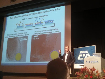
Here all pictures that appear on Twitter (#EuroCVD), Facebook, LinkedIn or that people send me (jonas.sundqvist@baldengineering.com) will be collected!
Main page of Euro CVD 20 : http://eurocvd20.empa.ch/index.html 

Impressions


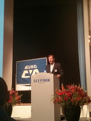
Prof. Hoffman opening the Euro CVD and the famous CVD flag hanging in the background (Photo by Henrik Pedersen)


HERALD Flyers! (Twitter, Henrik Pedersen)


Hoffman and Devi presented HERALD (Twitter, Henrik Pedersen)


Michael Hitchman makes a big announcement: after 20 years, he will retire as the editor of the journal CVD (Twitter, Sean Barry)


Seminars


Don´t miss the talk by Henrik Pedersen, Department of Physics, Chemistry and Biology, Linköping University, making an effort to unite us all "A combined ALD-CVD route for group 13 nitride based high frequency devices" Thursday 16 July, 09:30. Here a preview of the talk in the making (Twitter, Henrik Pedersen).


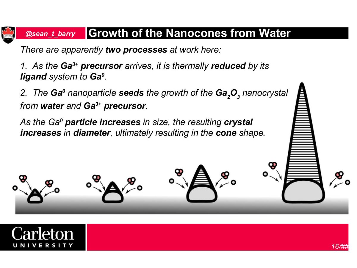
Preview slide from Sean Barry "Growth of Nanocones from Water" (shared on Twitter)


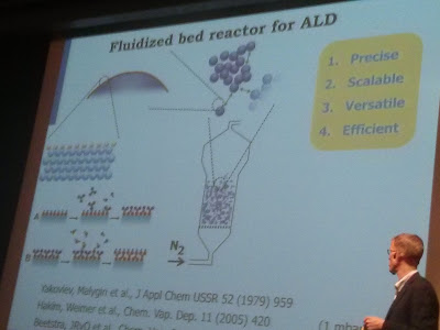
Ruud van Ommen giving his talk on ALD on nano powders using Fluidized bed reactors first publish in Russia 1979 (Photo by Henrik Pedersen)


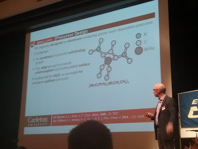
Talk by Sean Barry on seedless GaO nano wire growth by pulsed CVD (Photo by Henrik Pedersen)


New ketoiminate Y precursors from Devi's group and for yttria stabilized cubic hafnia by ALD and post deposition anneal (Twitter, Henrik Pedersen)


The talk by Prof. Pedersen from Linköping University on combining ALD and CVD for InN (Twitter, Sean Barry)


Ending of Euro CVD Twenty by Prof. Hoffmann (Twitter, Louise)


Poster sessions


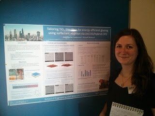
Ann-Louise Andersson at her poster on TiO2 AACVD / Hybrid CVD using surfactants (Photo by Henrik Pedersen)

Trade show


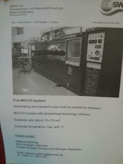
Free Aixtron MOCVD System (Henrik Pedersen)

Dinners and Receptions


Mini golf tournament (Twitter, Russell Binions)


Sightseeing


Sempach is a cute little town (Sean Barry, Twitter).


The gathering of ducks in the CVD Duck Pond - Euro CVD!  (Picture by Sean Barry, from Twitter)


A typically Swiss picture (Twitter, Russel BinIons)


Scenic Sempach (Twitter, Sean Barry)


Local gun shop  (Henrik Pedersen)


Boat cruise on the Sempach Lake (Henrik Pedersen)


Monday, June 22, 2015

Pegasus - New UK ALD and CVD Precursor company


Pegasus Chemicals is a privately owned UK company focused on localised support of the European ALD and CVD community with our ability to supply specialist chemicals, packaged for individual applications. We specialise in the high purity transfil and manufacture of small scale products for niche applications. Our product portfolio is wide and varied with specific focus on intrinsic purity and consistency. Our technical and product application knowledge in ALD and CVD has been honed through the manufacture and supply of specialist chemistry with many years experience. Our technical service team is available to discuss your deposition requirements to tailor the product with the application. 

www.pegasuschemicals.com 

Monday, June 8, 2015

IBM Zurich present III-V on silicon wafers breakthrough technology using ALD

IBM has done it - a method of depositing ultra-fast III-V nanowires suitable for transistor channels and other structures on silicon-on-insulator (SOI) substrates -  and for sure ALD was involved in one of the early crucial processing steps to create the template for TASE - Template Assisted Selective Epitaxy. 

"A 30-nm-thick SiO2 layer covering the entire structure was conformally deposited using atomic layer deposition (ALD) " 

Check out the details below and in the Open Access paper!

Template-assisted selective epitaxy of III–V nanoscale devices for co-planar heterogeneous integration with Si (Open Access)

H. Schmid, M. Borg, K. Moselund, L. Gignac, C. M. Breslin, J. Bruley, D. Cutaia and H. Riel
Appl. Phys. Lett. 106, 233101 (2015); http://dx.doi.org/10.1063/1.4921962 


Schematic (a) and SEM images (b)–(d) illustrating stacking of Si and III-V NWs. (b) SEM image shows a tilted view of three stacked template structures. (c) SEM cross-section image of the Si NW stack and (d), TEM image of the GaAs NW stack (Appl. Phys. Lett. 106, 233101 (2015); http://dx.doi.org/10.1063/1.4921962)

III–V nanoscale devices were monolithically integrated on silicon-on-insulator (SOI) substrates by template-assisted selective epitaxy (TASE) using metal organic chemical vapor deposition. Single crystal III–V (InAs, InGaAs, GaAs) nanostructures, such as nanowires, nanostructures containing constrictions, and cross junctions, as well as 3D stacked nanowires were directly obtained by epitaxial filling of lithographically defined oxide templates. The benefit of TASE is exemplified by the straightforward fabrication of nanoscale Hall structures as well as multiple gate field effect transistors (MuG-FETs) grown co-planar to the SOI layer. Hall measurements on InAs nanowire cross junctions revealed an electron mobility of 5400 cm2/V s, while the alongside fabricated InAs MuG-FETs with ten 55 nm wide, 23 nm thick, and 390 nm long channels exhibit an on current of 660 μA/μm and a peak transconductance of 1.0 mS/μm at VDS = 0.5 V. These results demonstrate TASE as a promising fabrication approach for heterogeneous material integration on Si.


SEM images illustrating epitaxial filling of complex nano structures. (a) Evolution of the growth during filling of three templates, each having a lithographically pre-defined constriction. (b) Formation of an InAs cross-junction for the later fabrication of a Hall structure. The InAs film thickness is 23 nm (Appl. Phys. Lett. 106, 233101 (2015); http://dx.doi.org/10.1063/1.4921962).


The fabrication steps of TASE : a (100)-oriented SOI substrates (Soitec) with a device layer thickness of 25–50 nm were patterned using e-beam lithography and reactive ion etching. A 30-nm-thick SiO2 layer covering the entire structure was conformally deposited using atomic layer deposition (ALD) and annealed at 850 °C in Ar/H2. The SiO2 cap on one end of the Si structure was opened by patterning polymethylmethacrylate (PMMA) by e-beam lithography and buffered hydrofluoric acid (BHF) etching to expose the Si device layer. Next the Si was back-etched to the desired length using either XeF2 dry etching followed by tetramethylammoniumhydroxide (TMAH) wet etching or TMAH etching only, to result in well-defined {111} planes. The orientation of the {111} planes with respect to the channel direction was controlled by the alignment of the channel patterns. All structures reported here were patterned along the 〈110〉 direction. The as-prepared substrate was dipped in diluted (2.5%) HF to remove the native oxide on the exposed Si surfaces within the channels and was immediately loaded into the MOCVD reactor. Selective epitaxy of InGaAs was carried out using trimethylindium (TMIn), tertiarybutylarsine (TBAs), and trimethygallium (TMGa) at V/III ratio = 40 with TMIn/(TMIn+TMGa) = 0.5 at 580 °C. Chemical analysis was obtained from electron energy loss spectroscopy (EELS) analysis and indicated an In0.50Ga0.50As composition. InAs epitaxy was carried out at 520 °C using TMIn and TBAs with a V/III ratio = 80 and V/III ratio = 40 for the MuGFETs, respectively. Optionally, the dielectric template was removed after growth by wet etching in diluted HF, to expose the Si–III-V nano-structure on the SiO2 layer (BOX).