Showing posts with label High-k. Show all posts

Tuesday, June 27, 2017

The Dubbo Project - The High-k mine in Dubbo, NSW Australia

Unknowingly I´ve been camping and going through in Dubbo two times, literally our tent was on top of a high-k mine without me knowing it! They have got it all there Down Under: zirconium, hafnium, niobium, tantalum and all of the rare earths. Just take a moment to check out the videos below and stay tuned for more on the Dubbo project.


The Dubbo Project (DP) is a new and strategically significant source of high demand critical metals, which are independent of traditional supply sources. The Dubbo resource is a long life polymetallic ore body that is readily processed and separated into valuable products including zirconium, hafnium, niobium and rare earths.


A large scale Demonstration Pilot Plant at ANSTO in Sydney has been operating since 2008 to provide robust qualification and optimisation of the DZP process and the necessary information for scale up to a full scale operating plant. The plant has proven the process flowsheet from a chemical and engineering sense as well as providing capital and operating costs for scale-up.
 

Over 100 tonnes of ore has been processed in the Demonstration Pilot Plant to produce zirconium, hafnium, niobium and rare earth products.

At a processing rate of 1 m tpa of ore for the full scale plant, annual revenue for the four product groups ranges from US$430m - US$470m pa with an EBITDA of $235m - $275m pa.

Picosun’s ALD solutions enable non-volatile memories (ReRAM)

As previously reported here (LINK) New prospects for universal memory from MIPT Russia using Picosun ALD: ESPOO, Finland, 27 June, 2017 – Picosun Oy, leading supplier of high quality Atomic Layer Deposition (ALD) thin film coating solutions, reports of breakthrough results achieved with its ALD technology in development of novel high-speed memories. These memories are required in state-of-the-art data storage applications, where a combination of very large capacity and extremely fast operating speed is needed. The results have been obtained at Picosun’s long-term customer Moscow Institute of Physics and Technology (MIPT), Russia.


Experimental cluster, including a Picosun ALD reactor, for growing and studying thin films in a vacuum at the Center of Shared Research Facilities, MIPT

ReRAM (Resistance Switching Random Access Memory) is a new, non-volatile memory type which has the attributes to become the much sought-after universal memory to replace and outperform the current technologies, and to solve the ever-growing demand for more and more efficient data storage systems. ReRAM is fast, small, structurally simple, it has high capacity and it operates at low voltages. These features help to decrease the device size, power consumption, and response time, allowing yet smoother-operating electronic end products. Smaller operating voltage enables ReRAM integration also to low-power devices such as portable, wearable, and mobile electronics, remote sensing and IoT (Internet of Things) applications, the number of which is growing explosively at the moment.

Wednesday, January 25, 2017

The NaMLab Novel High k Application Workshop 2017 in Dresden

NaMLab invites to the Novel High-k Application Workshop on March 9th and 10th, 2017. New challenges offered by the application of high-k dielectric materials in micro– and nanoelectronics will be discussed by more than 80 participants from industry, research institutes and universities. One main focus will be on the ferroelectric properties of HfO2. 

 
NaMLab created with the workshop a stimulating platform for application-oriented scientist to exchange ideas and discuss latest experimental results on MIM-capacitors, process technology, leakage & reliability as well as characterization of high-k dielectrics integrated in silicon based micro– and nanoelectronics. The ferroelectric properties of doped HfO2 and ZrO2 were discovered 10 years ago. On the second day of the workshop, root causes for the formation of this so far unknown phase will be discussed.

Registration for the workshop started:
- registration rate: participants: 12€/day  - students: 10€/day  (includes all meals and coffee breaks)
- registration rate can be paid by credit card, pay pal (Europe only: direct transfer)


Preliminary agenda:    March 9th  to 10th
Workshop location: Max Planck Institute PKS (Physics of Complex Systems), Noethnitzer Strasse 38

Sponsors:
  http://www.oxford-instruments.com/  
   http://www.strem.com/
  http://globalfoundries.com/

Co-organized by:

Monday, December 12, 2016

ALD of High-k using molecular oxygen at Stanford Nanofabrication Facility

The Stanford Nanofabrication Facility (SNF) is administarting a fantastic Wiki for their clean room equipment and processeses in nanofabrication. The Wiki is there for the SNF lab community as a resource and also as historical archive as stated in the Wiki description. For all us not part of SNF it is nice that a login is not needed to view public information available.

In the wiki you will find vast process archives for the tools operated and for us ALD people the ALD section is especially interesting to study. As listed SNF is operating 4 ALD Tools all from Ultratech CNT : one Savannah and three Fiji´s.

SNF ALD Wiki  : LINK

SNF list of available films : LINK

Recently SNF published a great review of their metal alkyl amide High-k PEALD processes and the good news is that it is open source easily available for all of us to study.
 

Atomic layer deposition by reaction of molecular oxygen with tetrakisdimethylamido-metal precursor

J Provine, Peter Schindler, Jan Torgersen, Hyo Jin Kim, Hans-Peter Karnthaler and Fritz B. Prinz

J. Vac. Sci. Technol. A 34, 01A138 (2016); http://dx.doi.org/10.1116/1.4937991

Wednesday, October 26, 2016

UPDATE : Transition metal compounds, Belux2 - 17-18 November 2016 - imec Belgium

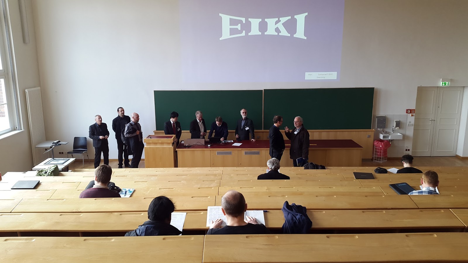
Registration for the workshop is still open: http://www2.imec.be/be_en/education/conferences/belux2.html. Many of imec's large industrial IDM partners and equipment suppliers have registered for this workshop - an excellent opportunity to meet the experts in this field!

 
Imec and the COST action HERALD will host a workshop dedicated to Transition metal compounds driving technological advancement. The Belux2 workshop will take place at imec in Leuven, Belgium on 17-18 November 2016.

 This 2 half-day workshop will provide an excellent opportunity to spark multidisciplinary discussions regarding the modeling, deposition and characterization of novel transition metal compounds for next generation technologies.

The program will consist of Presentations by invited speakers.
  
Prof. Atsufumi Hirohata (University of York, UK) - Heusler Alloy Films for Spintronic Devices
Dr. Stanislav Chadov (Max Planck, Germany) - Room-temperature tetragonal noncollinear antiferromagnet: Pt2MnGa
Prof. Andreas Michels (University of Luxembourg, Luxembourg) - Magnetic Neutron Scattering Studies on Nd-Fe-B Magnets
Prof. Thibault Devolder (Universite Paris Sud, France) - Nanosecond-Scale Switching in Perpendicularly Magnetized STT-MRAM Cells
Prof. Jens Kreisel (Luxembourg Institute of Science and Technology, Luxembourg) - Strain & phase transitions in oxide heterostructures and ultrathin films
Prof. Sebastiaan van Dijken (Aalto University, Finland) - Electric-Field Control of Magnetism in Multiferroic Heterostructures
Prof. Guus Rijnders (University of Twente, The Netherlands) - Piezeoelectrics
Geoffrey Pourtois (imec, Belgium) - Modeling of the impact of the chemical environment on the properties of MX2 materials for nanoelectronic applications
Stephen McDonnell (University of Virginia, US) - Deposition of and on 2D materials
Dr. Ageeth Bol (Eindhoven University, The Netherlands) - Atomic layer deposition of metals and oxides on graphene for future nanoelectronics
Prof. Alexander Shluger (University College London, UK) - Some ideas on the mechanisms of electroforming in oxides from DFT simulations
Dr. Uwe Schroeder (Namlab, Germany) - HfO2 and ZrO2 based ferroelectric materials for non-volatile memory applications
Prof. Matthias Wuttig (RWTH Aachen, Germany) - Novel Phase Change Materials by Design: The Mistery of Resonance Bonding
Dr. Ilia Valov (FZ Juelich, Germany) - Interfaces, Mobile Ions and Moisture Effects in ReRAM memristive systems
·         Poster session.
  • Walking dinner.
More information and the registration form are available at: http://www2.imec.be/be_en/education/conferences/belux2/home.html.
The fee for the workshop is only 50 euro (VAT included). The deadline for registration is 11 November 2016.
Poster contributions are welcome by abstract submission (http://www2.imec.be/be_en/education/conferences/belux2/call-for-papers.html). The deadline for abstract submission is 4 November 2016.
We really look forward to welcoming you at imec!
Best regards from the Belux2 organizing committee.
Naoufal Bahlawane, Luxembourg Institute of Science and Technology (LIST)
Sven Van Elshocht, imec (chairman)
Christoph Adelmann, imec
Annelies Delabie, imec
Johan Swerts, imec
Kathleen Vanderheyden, imec
Fred Loosen, imec
Please forward this email to whom it may concern.
http://www2.imec.be/content/user/Image/events/HERALD-LOGO-(PRIMARY).png
http://www2.imec.be/content/user/Image/events/logo_cost.png

Wednesday, October 5, 2016

CNR-IMM Italy employes Sentech SI PEALD LL for new high-k materials

SENTECH Instruments GmbH of Berlin, Germany says that the Institute for Microelectronics and Microsystems (CNR-IMM) in Catania – which is part of the Physics and Matter Technologies Department (DSFTM) of the National Research Council of Italy (CNR) - is using an SI PEALD LL plasma-enhanced atomic layer deposition tool with an 8-inch wafer configuration to investigate the integration of novel high-k gate dielectrics and passivating layers on devices based on gallium nitride (GaN) and other wide-bandgap semiconductors. 


The picture above shows the SI PEALD LL in the CNR-IMM cleanroom. (picture released by Sentech)

SENTECH says that its proprietary true remote CCP (capacitively coupled plasma) source is especially suited to such low-temperature and no-damage applications. The special design of the plasma source allows only radicals to reach the wafer surface, whereas high-energy photons and ions are completely blocked.

In conjunction, IMM and SENTECH have signed a joint development agreement (JDA) with the aim of the developing and characterizing laminated layers. The use of alternative high-k materials enables the shrinking of devices while maintaining their capacitance and reducing the leakage current density. In particular, the growth of Al2O3-HfO2 laminated layers is among the most often used combinations for such applications.


"The SENTECH SI PEALD LL reactor is a high-performance and flexible system, allowing the production of several high-quality dielectric thin films, whose physical properties can be tailored upon changing their chemical composition," says Dr Raffaella Lo Nigro, who is the scientist in charge of the SI PEALD LL tool and of cooperation with SENTECH. Nigro has wide-ranging expertise in the synthesis of binary and complex thin films by chemical vapor deposition (CVD) methods for several microelectronic applications. "Possible applications of this activity are related not only to the integration of novel gate dielectrics and passivating layers on wide-bandgap semiconductors but also for RF devices based on graphene," he adds.

The results of this work have already been published in scientific papers (Raffaella Lo Nigro, Emanuela Schilirò, Giuseppe Greco, Patrick Fiorenza and Fabrizio Roccaforte, Thin Solid Films, vol601, 2016, p68-72). Nanolaminated Al2O3-HfO2 and Al2O3/HfO2 bilayer thin films have been grown by PEALD on silicon substrates. Morphological, crystalline and electrical properties of the layer stacks were analyzed after low-temperature deposition and high thermal treatment. The highly stable deposition of single films and multi-layer laminates using SENTECH PEALD together with very good uniformity of the deposition process over the whole wafer are essential prerequisites for applications such as designing new high-k dielectrics, says the firm.

Friday, June 24, 2016

Harvard University initiates ALD patent infringement suits towards US chip makers

Harvard University initiates patent infringement suits to protect inventors’ rights in atomic layer deposition alkyl amide precursor used for High-k applications like DRAM and other high aspect ratio capacitor based technologies. 


Harvard has now filed patent-infringement suits against two major US chip makers, Micron and Globalfoundries. The University believes that these companies have violated patents that claim inventions created in Gordon’s lab of famous ALD Prof. Roy Gordon.
 
The article in The Harvard Gazette reports:
 
Over a few years, Gordon, his graduate students Jill Becker [Founder of Cambridge Nanotech] and Dennis Hausmann [Lam Research], and postdoctoral fellow Seigi Suh [DuPont] would play central roles in making that high-k dielectric insulator work. Their primary innovation, filed at the U.S. Patent Office in 2000 and described in scientific papers in 2001 and 2002, was to create a novel carrier molecule, one never before seen outside of Gordon’s lab, as well as to identify a class of precursor molecules ideally suited to use in a method called atomic layer deposition (ALD) to create thin films. This precursor molecule delivered the insulator where it had to go. Once there it released the metal atoms to form a uniform layer, while its other components — such as carbon, nitrogen, and hydrogen — were easily removed, leaving behind the pure insulator layer.

Isaac T. Kohlberg, Harvard’s senior associate provost, said it’s important that Harvard protect the intellectual property rights of faculty, postdoctoral researchers, students, and the University itself, particularly in an era when corporations increasingly look to academia for significant advances in science, engineering, and technology.

Here you can read the whole intriguing story from Gordon Lab in the Harvard Gazette : Defending breakthrough research. Here is also one of the well cited publications form 2002 on using TEMAHf and TEMAZr and water in deep trench DRAM stuctures (from Infineon) by Hausman et al : http://faculty.chemistry.harvard.edu/files/gordon/files/aldhf_3.pdf

There are many angles to this story and it will be interesting to follow this case.

Thursday, June 16, 2016

Imec Demonstrates Gate-All-Around MOSFETs with Lateral Silicon Nanowires at Scaled Dimensions

LEUVEN, Belgium – June 16, 2016 – Today, at the 2016 Symposia on VLSI Technology & Circuits, nano-electronics research center imec presented gate-all-around (GAA) n- and p-MOSFET devices made of vertically stacked horizontal silicon (Si) nanowires (NWs) with a diameter of only 8-nm. The devices, which were fabricated on bulk Si substrates using an industry-relevant replacement metal gate (RMG) process, have excellent short-channel characteristics (SS = 65 mV/dec, DIBL = 42 mV/V for LG = 24 nm) at performance levels comparable to finFET reference devices.

TEM images of an NMOS GAASiNWFET(LG=70nm):(a)overview of the SiNW array; (b)detailed view of two stacked SiNWs.

 
GAA devices architectures offer optimal electrostatic control, thereby enabling ultimate CMOS device scaling. In addition, horizontal NWs are a natural extension of RMG finFETs, in contrast to vertical NWs which require more disruptive technology changes. Furthermore, stacking of NWs maximizes the drive current per footprint. Imec successfully combined these three aspects, and, for the first time, demonstrated vertically stacked horizontal Si NWs at scaled dimensions: 8-nm-diameter wires, 45-nm lateral pitch, and 20-nm vertical separation.

Compared to the conventional bulk FinFET flow, imec implemented two major differences in the process flow. First, shallow trench isolation (STI) densification at 750°C resulted to preserve sharp silicon-germanium (SiGe)/Si interfaces, which is essential for well-controlled Si NW release. Second, a low-complexity ground plane doping scheme was applied, suppressing the bottom parasitic channel.

“By demonstrating stacked nanowires with solid electrostatic control, at scaled dimensions, and using an industry-relevant RMG process on bulk silicon substrates, imec has achieved breakthrough results that can pave the way to realizing sub-10nm technology nodes,” stated Dan Mocuta, Director Logic Device and Integration at imec. “The upcoming research phase will focus on achieving even denser pitches and on leveraging this knowledge to develop gate-all-around lateral nanowire CMOS devices.”

Imec’s research into advanced logic scaling is performed in cooperation with imec’s key partners in its core CMOS programs including GlobalFoundries, Intel, Micron, SK Hynix, Samsung, TSMC, Huawei, Qualcomm and Sony.

Tuesday, April 12, 2016

Room Temperature ALD of ZrO2 by Plasma Excited Water Vapor to be presented at ECS 229

Here is a cool upcoming presentation! Room temperature ALD of ZrO2 by using plasma excited water vapor (!) is to be presented at ECS Meeting in San Diego May 30 by K. Kanomata from Yamagata University, CREST, Japan. I can´t remember seeing Plasma activated water being used for ALD before - genius! This should be really useful for capacitors and transistors integrated on flexible electronics and displays.

RT Atomic Layer Deposition of ZrO2 By Using Plasma Excited Water Vapor

Monday, 30 May 2016: 12:10
Sapphire 410 A (Hilton San Diego Bayfront)
K. Kanomata (Yamagata University, CREST, JST), K. Tokoro, T. Imai, P. P. Pansila, M. Miura (Yamagata University), B. Ahmmad (Yamagata University,, CREST, JST), S. Kubota (Yamagata University, CREST, JST), K. Hirahara (Yamagata University), and F. Hirose (Yamagata University, CREST, JST)
 
Size of semiconductor devices in large-scale integration has reached the submicron range where gate oxide films in metal oxide semiconductor (MOS) devices need to be fabricated at a nanometer scale. Atomic layer deposition (ALD) is a technology for depositing dielectric films with monolayer precision by repeating adsorption of a source gas on substrate that is subsequently reactivated for further adsorption [1]. Zirconium oxide (ZrO2) is believed to be a candidate as the high-k gate oxide material [2]. The growth temperature for the ZrO2 deposition has been desired to be decreased to near room temperature (RT) because the interfacial layer is formed by the solid phase reaction with heating process [3]. In this work, we developed a RT atomic layer deposition of ZrO2 with tetrakis (ethylmethylamino) zirconium (TEMAZ) and a remote-plasma excited water vapor.


Thursday, April 7, 2016

Samsung Starts Mass Producing Industry’s First 10-Nanometer Class DRAM

Samsung just announced that they start Mass Producing Industry’s First 10-Nanometer Class DRAM now. According to the press release (here) the key technology developments include:
  • improvements in proprietary cell design technology
  • QPT - quadruple patterning technology lithography 
  • Ultra-thin dielectric layer deposition.
The two later ones should mean a lot of ALD business for High-k, Electrodes and dielectric spacers.

Below is a DRAM Technology Roadmap published by TechInsights last summer and here you can see that Samsung is nailing it and next we should expect announcements from SK Hynix and The Micron Camp.


Here is an earlier post form IEDM 2015 in December when Samsung revieled some details - if thoose are used here is unknown so hopefully some reverse engineering study will surface next:

Samsung to present low cost manufacturing of 20 nm DRAM and beyond at IEDM2015

Some advancement in keeping low cost manufacturing of 20 nm DRAM will be presented by Samsung at IEDM 2015. Key elements are:

  • avoiding EUV lithography
  • honeycomb structure (see figure below)
  • air-spacer technology


According to Solid State Technology an air-gap spacer arrangement achieves a 34% reduction in bitline capacitance for faster operation.

20nm DRAM: A New Beginning of Another Revolution (Invited), J. Park, Y.S. Hwang, S.-W. Kim, S.Y. Han, J.S. Park, J. Kim, J. W Seo, B.S. Kim, S.H. Shin, C.H. Cho, S.W. Nam, H.S. Hong, K.P. Lee, G.Y. Jin, and E.S. Jung, Samsung Electronics Co.


For the first time, 20nm DRAM has been developed and fabricated successfully without EUV lithography using the honeycomb structure and the air-spacer technology. These low-cost and reliable schemes are promising key technologies for 20nm technology node and beyond.


Monday, March 14, 2016

Photo show NaMLab Novel High-k Materials Workshop in Dresden

Novel High k Application Workshop 2016

In collaboration with the EU COST networking project HerALD (working group 4), NaMLab invites to the Novel High-k Application Workshop on March 14th and 15th, 2016. New challenges offered by the application of high-k dielectric materials in micro– and nanoelectronics will be discussed by more than 80 participants from industry, research institutes and universities. NaMLab created with the workshop a stimulating European platform for application-oriented scientist to exchange ideas and discuss latest experimental results on MIM-capacitors, process technology, leakage & reliability as well as characterization of high-k dielectrics integrated in silicon based micro– and nanoelectronics. In addition, new results in the field of ALD dielectrics in solar cells, transparent conduction oxides (TCOs) and atomic layer etching (ALE) will be discussed. 

Here are pictures from the Event - Day 1:

Networking / Breaks:


Two of the Sponsors of the event Jamal Belgacem from Strem and Andy Stamm Oxford Instruments


The Precursor Buffé from Strem 


Additional sponsors of the event - Sara Wengström from Swedish FAB Support and Paul Williams from Pegasus disussing precursors with very important customers.

Sessions :

 The speakers lining up with USB sticks to upload their presentations


Dr. Karim Cherkaoui, Nanoelectronic Materials and Devices Group (NMD), Tyndall National Lab, Ireland giving a talk on High-k on III/V semiconductors. 

 
J. Roberts from University of Liverpool - Dielectrics for AlGaN/GaN MISHEMT power electronics 


Dr. Jurgen Schubert Peter Grünberg Institute (PGI-9), Forschungszentrum Jülich - Rare eath oxides on GaN


N. Szabo, NaMLab, Dresden - ALD Al2O3 as a high‐k dielectric material for future GaN power devices.


Max Drescher, Fraunhofer IPMS, Dresden - Deciphering Reliability in High‐K Metal Gate Technology. 


Dr. Elke Erben, Globalfoundries, Dresden - Workfunction tuning and gate stack for 22nm FD‐SOI.


Felix Winkler, TU Dresden - Novel vertical TSV field effect transistor using ALD high‐k gate dielectrics


A. Thomas, IFW Dresden - ALD deposited HfO2‐based magnetic tunnel junctions 

 
M. Godlewski, Acad. of Sc. Warsaw, Poland - High‐k oxides by ALD ‐ from applications in electronics to biology and medicine


J. Van Houdt, Imec - High-k in memory devices.


M.H. Park, SNU, Seol, South Korea - Current understanding of ferroelectricity and field‐induced‐ferroelectricity in (Hf,Zr)O2 films based on first order phase transition theory 


Saturday, February 13, 2016

ALD HfO2 HKMG FETs on CVD mono layer graphene channels on 200 mm glass wafers by Samsung

Samsung Advanced Institute of Technology and Samsung-SKKU Graphene/2D Center showcases ALD HfO2 high-k transistors on mono layer graphene channels using 200 mm glass wafers. The ALD Process is TEMAHf/H2O running at 200 C and they achieve a CET of ~1.5 nm from an array of top-gated metal-oxide-graphene field-effect transistors.
 
Check out the free to down load Nature Scientific Report below.

 
SAIT (Samsung Advanced Institute of Technology)

Thickness scaling of atomic-layer-deposited HfO2 films and their application to wafer-scale graphene tunnelling transistors. 

Seong-Jun Jeong, Yeahyun Gu, Jinseong Heo, Jaehyun Yang, Chang-Seok Lee, Min-Hyun Lee, Yunseong Lee, Hyoungsub Kim, Seongjun Park & Sungwoo Hwang
Sci. Rep. 6, 20907; doi: 10.1038/srep20907 (2016).


(a) Optical image of the MOG-FET arrays fabricated on a 6″ Si wafer and a schematic illustration showing the structure of the MOG-FET device. (b) Optical microscope image of a fabricated MOG-FET unit device. (c) Cross sectional TEM image showing the HfO2 gate dielectric layer with a thickness of ~5 nm (including the seed layer converted to a HfO2 layer) on monolayered graphene. (d) Statistical distribution of the sheet resistance of a monolayered graphene before and after the ALD of HfO2 with and without an e-beam-evaporated Hf seed layer. Representative electrical characteristics measured from the fabricated MOG-FET devices: (e) gate dielectric leakage current, (f) gate capacitance as a function of the frequency, and (g) transfer curve (ID-VG). (Sci. Rep. 6, 20907; doi: 10.1038/srep20907 (2016)., Creative Commons Attribution 4.0 International License)

The downscaling of the capacitance equivalent oxide thickness (CET) of a gate dielectric film with a high dielectric constant, such as atomic layer deposited (ALD) HfO2, is a fundamental challenge in achieving high-performance graphene-based transistors with a low gate leakage current. Here, we assess the application of various surface modification methods on monolayer graphene sheets grown by chemical vapour deposition to obtain a uniform and pinhole-free ALD HfO2 film with a substantially small CET at a wafer scale. The effects of various surface modifications, such as N-methyl-2-pyrrolidone treatment and introduction of sputtered ZnO and e-beam-evaporated Hf seed layers on monolayer graphene, and the subsequent HfO2 film formation under identical ALD process parameters were systematically evaluated. The nucleation layer provided by the Hf seed layer (which transforms to the HfO2 layer during ALD) resulted in the uniform and conformal deposition of the HfO2 film without damaging the graphene, which is suitable for downscaling the CET. After verifying the feasibility of scaling down the HfO2 thickness to achieve a CET of ~1.5 nm from an array of top-gated metal-oxide-graphene field-effect transistors, we fabricated graphene heterojunction tunnelling transistors with a record-low subthreshold swing value of <60 mV/dec on an 8″ glass wafer.

TSMC Belgium & Sweden demonstrate first un-strained InAs FinFETs

Researchers led by TSMC R&D Europe B.V. in Leuven Belgium (Imec) and Lund Sweden (Lund Nano Lab), claim the first demonstration of an unstrained indium arsenide (InAs) fin field-effect transistor (finFET) with 20nm fin height (Hfin) [R. Oxland et al, IEEE Electron Device Letters, published online 29 January 2016]. The team also included researchers from University of Glasgow in the UK, Texas State University in the USA, and TSMC in Taiwan.

The gate insulation consisted of 5nm ZrO2 deposited by ALD, yielding an 1.2 nm equivalent oxide thickness (EOT). 

 
(a) Layer structure used, showing the pseudomorphic InAlAs etch-stop layer and (b) process flow for fabrication of InAs finFETs, starting with first step after wafer growth. (Figure from Semiconductor Today)

Full story here by Mike Cooke in Semiconductor Today and the IEEE Electron Devices abstract below.

InAs FinFETs with Hfin = 20 nm fabricated using a top-down etch process

Oxland, R. Li, X. ; Chang, S. ; Wang, S. ; Vasen, T. ; Ramvall, P. ; Contreras-Guerrero, R. ; Rojas-Ramirez, J. ; Holland, M. ; Doornbos, G. ; Chang, Y. ; Macintyre, D. ; Thoms, S. ; Droopad, R. ; Yeo, Y. ; Diaz, C. ; Thayne, I. ; Passlack, M.

 IEEE Electron Device Letters, published online 29 January 2016

We report the first demonstration of InAs FinFETs with fin width Wfin in the range 25–35 nm, formed by inductively coupled plasma etching. The channel comprises defect-free, lattice-matched InAs with fin height Hfin = 20 nm controlled by the use of an etch stop layer incorporated into the device heterostructure. For a gate length Lg = 1 nm, peak transconductance gm,peak = 1430 µS/µm is measured at Vd = 0.5 V demonstrating that electron transport in InAs fins can match planar devices.

Tuesday, February 9, 2016

Sub 20nm DRAM High-k from NaMLab, RWTH, KU Leuven and Samsung

NaMLab in Dresden, RWTH Aachen,Germany, KU Leuven, Belgium and Samsung has quite successfully since some years been collaborating on further high-k development for sub 20 nm DRAM. The research is lead by Uwe Schröder (ex-Qimonda High-k Principal) and Kyhyo Cho from Samsung. Here is a recent paper on how to push the ZrO2 based high-k further to even lower CET and leakage performance by introducing SrO inter layer high-k. Please enjoy this open source publication - abstract is given below.

Instead of STO based high-k that is physically too thick to fit in a sub 20nm DRAM cell, two different new approaches to develop a new ZrO based DRAM capacitor stack are presented:

1) by changing the inter-layer material from AlO to SrO 
2) the exchange of the top electrode material from TiN to Pt 

Low leakage ZrO based capacitors for sub 20 nm dynamic random access memory technology nodes

Milan Pešić, Steve Knebel, Maximilian Geyer, Sebastian Schmelzer, Ulrich Böttger, Nadiia Kolomiiets, Valeri V. Afanas'ev, Kyuho Cho, Changhwa Jung, Jaewan Chang, Hanjin Lim, Thomas Mikolajick and Uwe Schroeder
J. Appl. Phys. 119, 064101 (2016); http://dx.doi.org/10.1063/1.4941537


During dynamic random access memory (DRAM) capacitor scaling, a lot of effort was put searching for new material stacks to overcome the scaling limitations of the current material stack, such as leakage and sufficient capacitance. In this study, very promising results for a SrTiO based capacitor with a record low capacitance equivalent thickness value of 0.2 nm at target leakage current are presented. Due to the material properties of SrTiO films (high vacancy concentration and low band gap), which are leading to an increased leakage current, a physical thickness of at least 8 nm is required at target leakage specifications. However, this physical thickness would not fit into an 18 nm DRAM structure. Therefore, two different new approaches to develop a new ZrO based DRAM capacitor stack by changing the inter-layer material from AlO to SrO and the exchange of the top electrode material from TiN to Pt are presented. A combination of these two approaches leads to a capacitance equivalent thickness value of 0.47 nm. Most importantly, the physical thickness of <5 nm for the dielectric stack is in accordance with the target specifications. Detailed evaluation of the leakage current characteristics leads to a capacitor model which allows the prediction of the electrical behavior with thickness scaling.

Monday, February 8, 2016

Cubic High-k HfO2 by ALD on high mobility Germanium channels

High mobility Germanium is one of the most promising channel materials for future Logic, perhaps even at 7nm. Here is an open source paper (see abstract below) on using TEMAHf/H2O process for growing high symmetry cubic HfO2 on high mobility Germanium channel. It´s a joint work by University of Tokyo, Japan, and Zhejiang University, China. Until now all silicon based channel gate dielectrics are typically performed by using the HfCl4/H2O process. However, now moving too alternate high mobility channel materials like Germanium, InGaAsand other III/Vs it seem that the gate stack people will revisit the MO-precursors again - interesting!

 
The Takagi-Takenaka group researches the post-scaling semiconductor devices for low-power LSI and on-chip optical interconnection for: Ge/III-V MOSFETs, Tunnel FETs, Si photonics, III-V CMOS photonics, Graphene photonics and 2D material electronics (from Takagi and Takenaka Group)

For those of you interested in additional information from the Takagi and Takenaka Group check out there excellent web pages here: http://www.mosfet.k.u-tokyo.ac.jp/index-e.html

Low temperature formation of higher- cubic phase HfO by atomic layer deposition on GeO/Ge structures fabricated by thermal oxidation  

R. Zhang, P.-C. Huang, N. Taoka, M. Yokoyama, M. Takenaka and S. Takagi
Appl. Phys. Lett. 108, 052903 (2016); http://dx.doi.org/10.1063/1.4941538

We have demonstrated a low temperature formation (300 °C) of higher- HfO using atomic layer deposition(ALD) on an thermal oxidation GeO interfacial layer. It is found that the cubic phase is dominant in the HfOfilm with an epitaxial-like growth behavior. The maximum permittivity of 42 is obtained for an ALD HfOfilm on a 1-nm-thick GeO form by the thermal oxidation. It is suggested from physical analyses that the crystallization of cubic phase HfO can be induced by the formation of six-fold crystalline GeOstructures in the underlying GeO interfacial layer.

Monday, February 1, 2016

Epiluvac and SAMCO to offer processing equipment for WBG materials in Nordic countries

As earlier reported here on the BALD Blog Epiluvac from Sweden and SAMCO from Japan has signed a collaboration deal. Now the to partners have signed an extened agreement to include distribution of SAMCO products in Scandinavia. Interestingly SAMCO also have an ALD product line. See also previous report on ALD here.


 Epiluvac’s EPI-1000X silicon carbide reactor.


SAMCO's new AL-1 ALD system.
 
As reported by Solid State Technology : Sweden-based SiC CVD developer and manufacturer Epiluvac AB has entered into a collaboration with SAMCO, a semiconductor process equipment developer and manufacturer based in Japan, in which Epiluvac will introduce new clients to SAMCO in Sweden, Norway, Finland and Denmark.


Bo Hammarlund, Chair , CEO, founder  of Epiluvac AB
 
SAMCO offers systems and services that revolve around three major technologies: 1) thin film deposition with PECVD, MOCVD and ALD systems, 2) microfabrication with ICP etching, RIE and DRIE systems, and 3) surface treatment with plasma cleaning and UV ozone cleaning systems.

“With this collaboration, Epiluvac and SAMCO are both acting as a one-stop solution,” says Bo Hammarlund, managing director of Epiluvac AB. “We offer our expertise to help customers decide upon the best combinations in terms of processing equipment for WBG materials, including both SiC and GaN materials.”

Friday, January 29, 2016

HERALD Novel High-k Workshop Call for abstracts until Jan 31, 2016 - Working Group 4 Event

Reminder: Call for abstracts until Jan 31, 2016 - Working Group 4 Event

In collaboration with the EU COST networking project HERALD, NaMLab invites to the ‘Novel High-k Application Workshop’ on March 14th and 15th, 2016. New challenges offered by the application of high-k dielectric materials in micro– and nanoelectronics will be discussed by more than 80 participants from industry, research institutes and universities. The workshop was initiated as a stimulating European platform for application-oriented scientists to exchange ideas and discuss latest experimental results on MIM-capacitors, process technologies, leakage & reliability as well as characterization of high-k dielectrics integrated in silicon based micro– and nanoelectronics. In addition, new results in the field of ALD dielectrics in solar cells, transparent conduction oxides (TCOs) and atomic layer etching (ALE) will be discussed.

A long list of speakers already confirmed their participation at the workshop. A preliminary program can be found here: http://www.namlab.com/news/events-1/novel-high-k-application-workshop.

To participate in the workshop, please apply by the end of January 2016 with a ½ page abstract (oral or poster) describing the work you would like to present. Mail your abstract to ALD@namlab.com

Since the HERALD project aims to promote participation from new EU member countries, additional travel grants (up to €300 per person) are available. If you would like to apply for a travel grant, please state this in your email.

COST Action MP1402 - HERALD
Hooking together European research in Atomic Layer Deposition