Showing posts with label Chipmetrics. Show all posts

Thursday, January 25, 2024

Chipmetrics Secures € 2.4 Million Seed Funding Round to Accelerate Product Innovation and Global Expansion.

24.01.2024– Joensuu, Finland: Chipmetrics Ltd, the Atomic Layer Deposition (ALD) technology company and a pioneer in 3D ultra-high aspect ratio test elements for metrology of semiconductor and advanced thin film material manufacturing, proudly announces the successful closure of a €2.4 million investment round. The international investor syndicate was led by High-Tech Gründerfonds (HTGF) and co-led by OCCIDENT from Germany. Other investors were Innovestor, REDSTONE and BALD Engineering. This substantial investment serves as a testament to Chipmetrics’ groundbreaking advancements in the PillarHall® metrology test chip technology, positioning the company as a frontrunner in conformality measurements in material deposition processes. The funds raised will be instrumental in accelerating Chipmetric’s product development efforts, scaling production capabilities, and expanding its market presence with the already existing international customer base.


Founders and management team of Chipmetrics Ltd. Persons in the picture, from left to right: Feng Gao (CTO), Pasi Hyttinen (CDO) and Mikko Utriainen (CEO).


Mikko Utriainen, the visionary founder & CEO of Chipmetrics, highlights the investment’s role in driving the company’s innovative pursuits and global market expansion. “This investment is a boost for our growth plans and technological advancements. We are committed to enhancing our product portfolio, refine our measurement solutions, and reinforce our global sales network ” Utriainen states.

Olaf Joeressen, Senior Investment Manager of HTGF comments: “The team’s focus on delivering innovative solutions to their customers is impressive, and I look forward to more product and service innovations delivered by Chipmetrics!”

Investment manager Simon Schild von Spannenberg from OCCIDENT continues: “Chipmetrics has already established a reputable position in thin film process development with its innovative PillarHall® Lateral High Aspect Ratio (LHAR) test chips. Chipmetrics’ products convince with their unique user interface, precision, speed, and cost-efficiency in the complex 3D measurements. Our investment reflects our confidence in the Chipmetrics’ team and the success of the highly innovative technology on the global semiconductor market.”

About Chipmetrics

Chipmetrics Oy develops and delivers metrology solutions for manufacturing processes for the semiconductor industry. The company’s business is based on the sale of innovative metrology chips and measurement services whose applications are focused on ALD technology. The company’s main product is the PillarHall® metrology chip for thin film process conformality measurement. The company was founded in 2019 and its head office is in Joensuu, Finland. In addition, the company has employees and sales partners in Japan, South Korea, the USA, and Germany.

For more information, visit www.chipmetrics.com.

About High-Tech Gründerfonds

The seed investor High-Tech Gründerfonds (HTGF) finances tech start-ups with growth potential and has supported more than 700 start-ups since 2005. With the launch of its fourth fund, HTGF now has about 1.4 billion euros under management. Its team of experienced investment managers and start-up experts support young companies with expertise, entrepreneurial spirit and passion. HTGF’s focus is on high-tech start-ups in the fields of digital tech, industrial tech, life sciences, chemistry and related business areas. To date, external investors have injected about 5 billion euros of capital into the HTGF portfolio via more than 2,000 follow-on financing rounds. In addition, HTGF has already successfully sold shares in more than 170 companies. Fund investors in this public-private partnership include the German Federal Ministry for Economic Affairs and Climate Action, KfW Capital and 45 companies from a wide range of industries.

For more information at www.htgf.de.

About OCCIDENT

OCCIDENT is an international venture capital investor with offices in Munich and Zug, is owner-managed and invests its own assets. Its mission is to make a positive contribution to society through sustainable and meaningful investments. OCCIDENT invests in innovative deep tech start-ups with excellent technologies, broad application possibilities and the potential for further development in the fields of life sciences, industrial tech and digital. OCCIDENT acts as a long-term enabler for highly innovative startups and visionary founders.


About Innovestor

Innovestor is a Finnish investment company focusing on venture capital and real estate. In addition, we offer corporate venturing services. The firm currently manages six VC funds with total capital of over €250 million. Consisting of almost 100 growth companies across multiple sectors of technology and life science & health, it represents one of the largest private venture-backed portfolios in the Nordics. Our mission is to make good money.


About Redstone

Redstone, headquartered in Berlin with offices in Zurich and Helsinki, is a European early-stage venture capital firm that pursues selected investment strategies. With its data-driven approach, Redstone develops strong sector expertise, building valuable networks for its portfolio. As one of Europe’s most active early-stage investors, Redstone manages a diverse portfolio of over 80 companies, focusing on Built World, Climate, Fintech, Industrial Tech, Social Impact, and Quantum.

Contact Information:

Mikko Utriainen, CEO, Chipmetrics Ltd


Tel: +358 10 348 1344


Saturday, December 17, 2022

Kokusai Electric relies on patterned 3D substrates in thin film process metrology from Chipmetrics

Kokusai Electric is one of the leading semiconductor thin film process equipment manufacturers in the world. Recently, in the context of Japan Society of Applied Physics 69th Spring Meeting 2022, Kokusai presented their advanced thin film measurement and analysis concept used in their semiconductor process development.

The concept focuses on film thickness and localized film composition measurements from the special designed 3D patterned substrates, where the patterns are fine high aspect ratio structures.

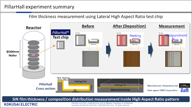
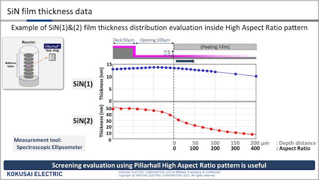
The average film thickness is obtained indirectly by measuring the mass change in the special 3D patterned wafer before and after the film depositions. The thickness accuracy is further improved by taking into account the high aspect ratio and wafer level non-uniformity measured by PillarHall® Lateral High Aspect Ratio (LHAR) test chips positioned on the carrier wafer. The PillarHall® measurement, enables easy screening after peeling off the top roof membrane and by measuring the film thickness distribution and conformality by the ellipsometer line-scanning measurements.

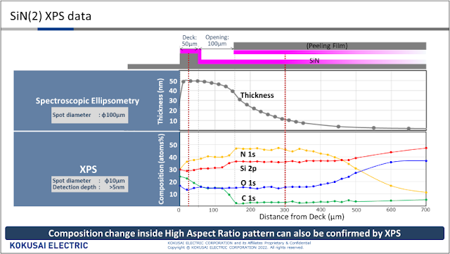
PillarHall® LHAR test chip has also another important function in Kokusai’s analysis concept. Namely, it is used for film elemental composition characterization along the trench wall in high aspect ratio structure. The measurement is carried out as a line-scan by XPS or SEM-EDS. For example, the characterization showed that two kinds of SiN processes behaved differently and Si/N composition changes along the high aspect ratio (AR>1000) trench were observed.


Figure 1. PillarHall experiment summary


Figure 2. SiN film thickness data


Figure 3. SiN(2) XPS data

Figures 1-3 show the PillarHall experimental set-up, data from the film thickness penetration depth profiles and XPS composition data of two kind of Kokusai’s SiN processes, SiN (1) and SiN (2).

Kenji Kameda and Akane Kitamura from Metrology Team, Kokusai Electric emphasized that:” It is difficult to obtain the analysis of thin films on high aspect ratio patterns without cross-sectional TEM. PillarHall is a simple and effective tool, it has fine patterns, and it enables us to use XPS and ellipsometer instead of TEM. Therefore, PillarHall is useful as an efficient measurement tool to improve Kokusai’s film forming technology.”

PillarHall LHAR test chip is a product of Chipmetrics Ltd, Finland. Chipmetrics CEO Dr. Mikko Utriainen reminds that any PillarHall data can be published without confidentiality concerns and the results are also well comparable between reactor systems and processes. The openness and accuracy of the ALD conformality data was one of the reasons why pioneering ALD scientists in Finland started to develop the PillarHall concept already in 2013.

Kokusai’s example shows that PillarHall is an efficient measurement tool and help to improve film forming technology for advanced semiconductor processes.

PillarHall is a product of Chipmetrics Ltd. Contact: info@chipmetrics, www.chipmetrics.com

Friday, September 16, 2022

The fast-growing technology start-up Chipmetrics moved to Photonics Center

(Original Article: LINK) In August, Photonics Center received a new business resident as Chipmetrics Oy moved to the centre's premises. Founded in 2019, the company has started its business rapidly: last year's turnover was already over EUR 700,000.

Chipmetrics’ CEO Mikko Utriainen is looking forward to testing Photonics Center’s potential as a research and development environment. The centre offers a range of equipment that is ideal for Chipmetrics’ needs, such as an ALD reactor, which can be used to test the functionality of products.

“It is also an enormous help to have the personnel of the University of Eastern Finland available for support at an hourly rate. Photonics Center’s equipment is demanding and requires highly skilled professionals. As a whole, the greatest benefit is certainly that all these resources are available in one place. No facilities of the same standard can be found in Eastern Finland; in fact, the only option in Finland would have been to transfer the company’s operations to Helsinki.”


Of the individual Photonics Center resources, the most important attraction factor for Chipmetrics was cleanrooms.

“The handling and development of our products must all be done in cleanrooms, as is typical in the semiconductor industry. That is why they are a necessity for a company like us.”

Measurement solution to increase efficiency in processes worth billions

Chipmetrics specialises in ALD technology. ALD stands for atomic layer deposition, which enablesmeans coating three-dimensional objects with thin film structures. ALD is a growing sector: according to Utriainen, the global market is approaching EUR 3 billion.

“ALD is used, for example, in semiconductor components, batteries and optical filters with 3D structures that are difficult to implement and coat. A smooth uniform thin film coating is very difficult, but it is even more difficult to measure whether the coating is really uniform smooth.”

Chipmetrics’ PillarHall solution is capable of very accurate measurement, enabling semiconductor manufacturers to enhance their own processes. Even small improvements can be valuable.

“The investments made by giant electronics companies are often in billions. A manufacturer of semiconductor equipment, which is best able to demonstrate its technical performance, can win a significantly sizeable deal in a big chip manufacturer’s factory investment. It is often important for our customer companies to be able to demonstrate to their own customers how well they can achieve a functioning process,” Utriainen explains.

Investors getting interested

Chipmetrics is a spinoff company that originated from a VTT research project. Utriainen was involved in the development of technology already at VTT. The company was established in 2019 and operational activities began at the end of 2020 when IPR rights were transferred to Chipmetrics.

The first full financial year was already good for the company: turnover was EUR 703,000 and profit was EUR 84,000. Chipmetrics just recently finished its start-upseed funding round, which netted EUR 340,000 for the company. The round was led by the North Karelia Growth Fund and four private investors. With the help of new funding, CEO Utriainen plans to develop the company’s product portfolio and expand the international sales network.

“ALD technology is complex, and it has been one of the key challenges for investors: sponsors naturally want to understand what they are participating in. We have now got investors involved in Finland, which also increases interest abroad.”

“It is our pleasure to welcome Chipmetrics to Photonics Center,” says Pauliina Pikkujämsä, Director of Business Services at Business Joensuu. “Photonics is one of the top industries in Joensuu, and Photonics Center is a direct investment in the operations of companies that manufacture or utilise photonics. ALD technology, the field of Chipmetrics, also has huge growth potential internationally. We’d like to have more such growth companies in the Joensuu region.”

Further information:

Pauliina Pikkujämsä

Business Services Director, Invest In and Relocation Services, pauliina.pikkujamsa@businessjoensuu.fi, +358 40,743 4362

Mikko Utriainen

Chipmetrics Oy, CEO, mikko.utriainen@chipmetrics.com, +358 40,753 7415


Business Joensuu

Business Joensuu Oy offers services for launching companies, growth and internationalisation, investing and setting up operations in an area, and space and event services of the Joensuu Science Park. Business Joensuu also produces growth and competitiveness programmes which create the best conditions for companies to operate in the Joensuu area.

Chipmetrics

Chipmetrics Oy is an ALD (Atomic Layer Deposition) technology company. Chipmetrics is the market leader in delivering productised nanotechnological high aspect ratio test structures to the semiconductor industry and emerging ALD applications. Chipmetrics’ headquarters are located in Joensuu. Further information: www.chipmetrics.com

Picture credits: Chipmetrics Oy

Monday, September 5, 2022

Chipmetrics announces completion of the seed investment round

Joensuu, Pohjois-Karjala Sep 4, 2022 (Issuewire.com) - Chipmetrics Ltd, the ALD (Atomic Layer Deposition) technology company and the market leader of productized 3D ultra-high aspect ratio test elements for semiconductor and advanced material manufacturing announced it has closed its 340.000 euro seed round. The investment round was led by Redstone through its North Karelia Growth Fund, alongside four private semiconductor and ALD experts.


“Our mission is to support our customers in the development of Atomic Layer Processes and their 3D applications by offering innovative, fast, and accurate measurement solutions. With this seed funding, we will develop our product portfolio and measurement concept offering and expand our global sales network.” Says Mikko Utriainen, Founder & CEO of Chipmetrics.

“I invested in Chipmetrics since I know the ALD market very well and Chipmetrics has clear potential to grow with the increasing adoption of ALD in the semiconductor industry,” says Jonas Sundqvist, a respected ALD consultant and entrepreneur from Dresden, Germany.

Other private investors, Matias Koski and James Song will support the company with their industry networks. Mr. Song will support building distribution in South Korea and beyond. Mr. Koski is based in Hong Kong, with a background in mobile phones and augmented reality.

Private investors also include Kai Seikku, a respected leader in the semiconductor industry, presently President and CEO of Okmetic and Vice General Manager & EVP of NSIG group.

Kaj Hagros, managing partner for Redstone Nordics and general partner for North Karelia Growth Fund comments: “Redstone’s existing collaborations with investors and corporations globally open opportunities for partnerships and business development. Chipmetrics has extraordinarily solid technology and a good market position, fully functional products already shipping, a great team, and clear plans to execute growth. Delighted to lead the round”.

Chipmetrics’ conformality measurement method based on PillarHall® Lateral High Aspect Ratio (LHAR) test chips has already gained a solid position in conformality measurements among ALD/CVD/BCD thin film process developers. The customers are leading semiconductor industry equipment suppliers and equipment users. The advantages of PillarHall® LHAR technology are a unique and convenient user interface, high accuracy and speed, and cost-effectiveness in challenging 3D measurements.

About Chipmetrics

Chipmetrics Ltd is an ALD (Atomic Layer Deposition) technology company founded in 2019. Chipmetrics is the market leader as a supplier of productized nanotechnological high aspect ratio test structures for the semiconductor industry and ALD applications. Chipmetrics' head office is in Joensuu, Finland, and it has sales representatives in Japan, South Korea, Taiwan, Singapore, China, and Germany. More information: www.chipmetrics.com

Mikko Utriainen, CEO, Chipmetrics Ltd

Email: mikko.utriainen@chipmetrics.com; tel. +358407537415

About Redstone

Redstone is a Berlin-based venture capital firm managing 10 sector funds with 360 closed transactions. Redstone is the general partner for North Karelia Growth Fund, investing in recently established and young companies from the region, particularly in the sectors of digitalization, forest and bio-economy, photonics, travel and creative industries, and material sciences. More information: www.redstone.vc

Kaj Hagros, Managing Partner, Redstone Nordics

Sunday, July 17, 2022

Chipmetrics High Aspect Ratio Test Chip launched at ALD2022 in Ghent

At the recent AVS ALD2022 Conference in Ghent, Belgium, I made several rounds in the ALD industrial exhibition and met up with Chipmetrics Oy from Finland. Chipmetrics produce test structures, chips, and wafer concepts for advanced materials and microelectronics manufacturing, many specifically for ALD. Their main product – PillarHall test chip – is developed for advanced thin film process conformality characterization to accelerate applications of conformal 3D thin films. The Pillar Hall test chip has a lateral, very high aspect ratio structure to determine conformality when developing new ALD hardware, processes, and precursors.


Chipmetrics at AVS ALD2022 in Ghent, Belgium (Lower photo: Zahra Ghaderi, Mikko Utriainen and James Song)

What caught my eye this time was their new vertical high aspect ratio test chip - VHAR1 silicon test chip which consists of an array of vertical high aspect ratio holes. The holes have a constant hole diameter of 1 μm, and a depth of 200 μm over the whole chip area 15 × 15 mm. The deposited film penetration depth profile can be measured by cross-sectioning as normally done with the vertical high aspect ratio test structures.

This structure resembles the situation in semiconductor devices such as DRAM, 3DNAND, and TSVs. It can undoubtedly get valuable information and understanding when developing ALD processes for large surface areas with high aspect ratios. Anyone that has developed new ALD processes knows that not only the aspect ratio plays a role but also the total surface area since you need to achieve a sufficient dose of the precursors at the right process conditions to achieve perfect conformality very fast to be productive and minimize precursor decomposition, "CVD effects" and have effective purging of precursors and ALD process byproducts.

For more information, please find contact information here to Chipmetrics: LINK


Links

PillarHall – introduction in SlideShare

PillarHall – introduction in YouTube

PillarHall – short introduction in YouTube

Video: How to use PillarHall test chip

PillarHall Web Site

About Chipmetrics:

Chipmetrics is a forerunner in productizing test structures, test chips, and wafer concepts for advanced materials and microelectronics manufacturing.

We are experts in thin film conformality characterization. Our main product – PillarHall test chip – is developed for advanced thin film process conformality characterization to accelerate applications of conformal 3D thin films.

Chipmetrics Oy is a part of the emerging Atomic Layer Deposition (ALD) industry and research community. Our headquarters are in Finland – in the country of the origin of ALD.