Showing posts with label 2d materials. Show all posts

Wednesday, November 18, 2015

Imec on taking 2D materials from lab to fab, and to technology

I just found this interesting article in Solid State Technology (abstract below) and realized again that 2D materials is actually steaming ahead and wafer level processing is happening today. Maybe 2D materials are to some extent even more promising than III/V channel integration on silicon wafers through horizontal or vertical Nanowires. One huge advantage as I see it is the lower thermal budget required for 2D Material growth or transfer processes which opens up huge possibilities for 3D stacking and continued scaling similar to what is happening for 3DNAND today.

Taking 2D materials from lab to fab, and to technology [Solid State Technology]

Due to their exciting properties, 2D crystals like graphene and transition metal dichalcogenides promise to become the material of the future.

BY STEFAN DE GENDT, CEDRIC HUYGHEBAERT, IULIANA RADU and AARON THEAN, imec, Leuven, Belgium.


The Technology roadmap as presented recently by Imec at the EWMOVPE workshop in Lund, Sweden, showing 2D materials as an option for beyond the 5 nm node.

As we enter into the era of functional scaling where the cross-roads of More-Moore and More-Than-Moore meet, the search for new devices and their enabling material comes to the forefront of technology research. 2D crystals provide very interesting form-factors with respect to traditional 3D crystals (bulk, Si, and III-V semiconductors). In this elegant 2D form, electronic structure, mechanical flexibility, defect formation, and electronic and optical sensitivity become dramatically different. Aaron Thean: “As researchers at imec explore the physics and applications of such material, it is now becoming important to find a wafer-scale path towards technology implementation and integration of these novel materials.” Working closely with research teams across universities and industry partners, the first important step for imec is to enable the flake-to-wafer transition, while concurrently exploring the material, and device-to-circuit applications. The work will build new infrastructure (e.g. epitaxy, metrology, patterning, and electrical characterizations, etc.) around it.

Continue reading in Solid State Technology

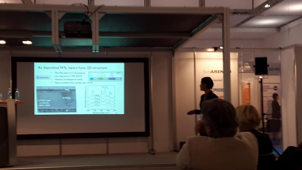
Interesting here is that imec is working on wafer level growth of MX2 materials "by a direct sulfurization process or by atomic layer deposition in the 200 and 300mm imec fabs.” This is not the first time that imec makes presentations in this area. I myself visited two events this year where imec presented work in this field - EWMOVPE workshop, Lund Sweden (above) and SEMICON Europa in Dresden (below).


Monolayer controlled deposition of 2D transition metal dichalcogenides on large area substrates, Presented by Annelies Delabie, Imec at SEMICON Europa 6th of October 2015, in Dresden.

I also visited SEMICON Europa 2014 where imec hosted a session on 2D Materials : http://www.semiconeuropa.org/node/2786 which was very interesting. However, there are probably some years of development ahead as ITRS has 5 nm introduction in the year 2020 or 2021 ready for mass production and that node will as we know it today not employ 2D materials.

Wednesday, July 22, 2015

Oak Ridge researchers make scalable arrays of building blocks for ultrathin electronics

OAK RIDGE, Tenn., July 22, 2015--Semiconductors, metals and insulators must be integrated to make the transistors that are the electronic building blocks of your smartphone, computer and other microchip-enabled devices. Today's transistors are miniscule--a mere 10 nanometers wide--and formed from three-dimensional (3D) crystals.


Complex, scalable arrays of semiconductor heterojunctions -- promising building blocks for future electronics -- were formed within a two-dimensional crystalline monolayer of molybdenum deselenide by converting lithographically exposed regions to molybdenum disulfide using pulsed laser deposition of sulfur atoms. Sulfur atoms (green) replaced selenium atoms (red) in lithographically exposed regions (top) as shown by Raman spectroscopic mapping (bottom). Credit : Oak Ridge National Laboratory, U.S. Dept. of Energy

But a disruptive new technology looms that uses two-dimensional (2D) crystals, just 1 nanometer thick, to enable ultrathin electronics. Scientists worldwide are investigating 2D crystals made from common layered materials to constrain electron transport within just two dimensions. Researchers had previously found ways to lithographically pattern single layers of carbon atoms called graphene into ribbon-like "wires" complete with insulation provided by a similar layer of boron nitride. But until now they have lacked synthesis and processing methods to lithographically pattern junctions between two different semiconductors within a single nanometer-thick layer to form transistors, the building blocks of ultrathin electronic devices.

Now for the first time, researchers at the Department of Energy's Oak Ridge National Laboratory have combined a novel synthesis process with commercial electron-beam lithography techniques to produce arrays of semiconductor junctions in arbitrary patterns within a single, nanometer-thick semiconductor crystal. The process relies upon transforming patterned regions of one existing, single-layer crystal into another. The researchers first grew single, nanometer-thick layers of molybdenum diselenide crystals on substrates and then deposited protective patterns of silicon oxide using standard lithography techniques. Then they bombarded the exposed regions of the crystals with a laser-generated beam of sulfur atoms. The sulfur atoms replaced the selenium atoms in the crystals to form molybdenum disulfide, which has a nearly identical crystal structure. The two semiconductor crystals formed sharp junctions, the desired building blocks of electronics. Nature Communicationsreports the accomplishment.

"We can literally make any kind of pattern that we want," said Masoud Mahjouri-Samani, who co-led the study with David Geohegan. Geohegan, head of ORNL's Nanomaterials Synthesis and Functional Assembly Group at the Center for Nanophase Materials Sciences, is the principal investigator of a Department of Energy basic science project focusing on the growth mechanisms and controlled synthesis of nanomaterials. Millions of 2D building blocks with numerous patterns may be made concurrently, Mahjouri-Samani added. In the future, it might be possible to produce different patterns on the top and bottom of a sheet. Further complexity could be introduced by layering sheets with different patterns.

Added Geohegan, "The development of a scalable, easily implemented process to lithographically pattern and easily form lateral semiconducting heterojunctions within two-dimensional crystals fulfills a critical need for 'building blocks' to enable next-generation ultrathin devices for applications ranging from flexible consumer electronics to solar energy."


Tuning the bandgap


"We chose pulsed laser deposition of sulfur because of the digital control it gives you over the flux of the material that comes to the surface," said Mahjouri-Samani. "You can basically make any kind of intermediate alloy. You can just replace, say, 20 percent of the selenium with sulfur, or 30 percent, or 50 percent." Added Geohegan, "Pulsed laser deposition also lets the kinetic energy of the sulfur atoms be tuned, allowing you to explore a wider range of processing conditions."

It is important that by controlling the ratio of sulfur to selenium within the crystal, the researchers can tune the bandgap of the semiconductors, an attribute that determines electronic and optical properties. To make optoelectronic devices such as electroluminescent displays, microchip fabricators integrate semiconductors with different bandgaps. For example, molybdenum disulfide's bandgap is greater than molybdenum diselenide's. Applying voltage to a crystal containing both semiconductors causes electrons and "holes" (positive charges created when electrons vacate) to move from molybdenum disulfide into molybdenum diselenide and recombine to emit light at the bandgap of molybdenum diselenide. For that reason, engineering the bandgaps of monolayer systems can allow the generation of light with many different colors, as well as enable other applications such as transistors and sensors, Mahjouri-Samani said.

Next the researchers will see if their pulsed laser vaporization and conversion method will work with atoms other than sulfur and selenium. "We're trying to make more complex systems in a 2D plane--integrate more ingredients, put in different building blocks--because at the end of the day, a complete working device needs different semiconductors and metals and insulators," Mahjouri-Samani said.

To understand the process of converting one nanometer-thick crystal into another, the researchers used powerful electron microscopy capabilities available at ORNL, notably atomic-resolution Z-contrast scanning transmission electron microscopy, which was developed at the lab and is now available to scientists worldwide using the Center for Nanophase Materials Sciences. Employing this technique, electron microscopists Andrew Lupini and visiting scientist Leonardo Basile imaged hexagonal networks of individual columns of atoms in the nanometer-thick molybdenum diselenide and molybdenum disulfide crystals.

"We could directly distinguish between sulfur and selenium atoms by their intensities in the image," Lupini said. "These images and electron energy loss spectroscopy allowed the team to characterize the semiconductor heterojunction with atomic precision."


Tuesday, July 7, 2015

Integration of Sub-10 nm ALD Gate Oxide on MoS2 with Ultra Low Leakage and Enhanced Mobility

Here is a nice Open Source report (Scientific Reports 5, Article number: 11921 (2015) doi:10.1038/srep11921) on integration of Sub-10 nm Gate Oxide on MoS2 with Ultra Low Leakage and Enhanced Mobility. 

Atomic layer deposition of Al2O3 on MoS2 flakes was performed according to the paper, some of the MoS2 flakes were loaded into the Picosun R200 ALD chamber for direct Al2O3 deposition. During the deposition, TMA and H2O served as the aluminum and oxygen precursors, respectively, and different growth temperatures and pulse time were adopted to observe their impacts. For some of the flakes, the remote O2 plasma pretreatments were carried out in the same chamber before Al2O3 was deposited.


(a) Cross-sectional schematic of the top-gated devices together with the electrical connections. (b) Ids – Vtg curves with Vds ranging from 50 mV to 500 mV. The inset shows the Ids – Vds curves with the top gate voltages of 0 V and 2 V. (c) Top gate leakage current of the device. Optical image of the top gate device is attached as the inset of (c). Top gate dielectric of this device is 60 cycles Al2O3 deposited with 60 s remote oxygen plasma pretreatment. All these measurements were performed at room temperature with the back gate grounded (Scientific Reports 5, Article number: 11921 (2015) doi:10.1038/srep11921) .

Tuesday, June 23, 2015

Chinese Labs produce Ultraclean and large-area monolayer hexagonal boron nitride on Cu foil by LPCVD

Researchers from The National Center for Nanoscience and Technology and Hubei University People's Republic of China has presented result on synthesis of large-area (4 × 2 cm2) high quality monolayer h-BN with an ultraclean and unbroken surface on copper foil by using LPCVD.


Monolayer h-BN, SAED diffraction and h-BN on SiO2/Si substrate (Source : http://nanotechweb.org/cws/article/lab/61589).

Ultraclean and large-area monolayer hexagonal boron nitride on Cu foil using chemical vapor deposition

Yao Wen, Xunzhong Shang, Ji Dong, Kai Xu, Jun He and Chao Jiang
2015 Nanotechnology 26 275601. doi:10.1088/0957-4484/26/27/275601

Atomically thin hexagonal boron nitride (h-BN) has been demonstrated to be an excellent dielectric layer as well as an ideal van der Waals epitaxial substrate for fabrication of two-dimensional (2D) atomic layers and their vertical heterostructures. Although many groups have obtained large-scale monolayer h-BN through low pressure chemical vapor deposition (LPCVD), it is still a challenge to grow clean monolayers without the reduction of domain size. Here we report the synthesis of large-area (4 × 2 cm2) high quality monolayer h-BN with an ultraclean and unbroken surface on copper foil by using LPCVD. A detailed investigation of the key factors affecting growth and transfer of the monolayer was carried out in order to eliminate the adverse effects of impurity particles. Furthermore, an optimized transfer approach allowed the nondestructive and clean transfer of the monolayer from copper foil onto an arbitrary substrate, including a flexible substrate, under mild conditions. Atomic force microscopy indicated that the root-mean-square (RMS) roughness of the monolayer h-BN on SiO2 was less than 0.269 nm for areas with fewer wrinkles. Selective area electron diffraction analysis of the h-BN revealed a pattern of hexagonal diffraction spots, which unambiguously demonstrated its highly crystalline character. Our work paves the way toward the use of ultraclean and large-area monolayer h-BN as the dielectric layer in the fabrication of high performance electronic and optoelectronic devices for novel 2D atomic layer materials.

Monday, June 22, 2015

Penn State - Diode a few atoms thick shows surprising quantum effect

As publish by Penn State : A quantum mechanical transport phenomenon demonstrated for the first time in synthetic, atomically-thin layered material at room temperature could lead to novel nanoelectronic circuits and devices, according to researchers at Penn State and three other U.S. and international universities.


Atomic multilayer structure of van der Waals solids representing layering with a graphene substrate.


Current-voltage curves of single junction (green) van der Waals solid (no NDR) and multijunction (red, orange) van der Waals solids (NDR). Stacking and choice of materials determines the location and width of peak.

The quantum transport effect, called negative differential resistance (NDR), was observed when a voltage was applied to structures made of one-atom-thick layers of several layered materials known as van der Waals materials. The three-part structures consist of a base of graphene followed by atomic layers of either molybdenum disulfide (MoS2), molybdenum diselenide (MoSe2), or tungsten diselenide (WSe2).

NDR is a phenomenon in which the wave nature of electrons allows them to tunnel through any material with varying resistance. The potential of NDR lies in low voltage electronic circuits that could be operated at high frequency.

“Theory suggests that stacking two-dimensional layers of different materials one atop the other can lead to new materials with new phenomena,” said Joshua Robinson, a Penn State assistant professor of materials science and engineering whose student, Yu-Chuan Lin, is first author on a paper appearing online today, June 19, in the journal Nature Communications. The paper is titled “Atomically Thin Resonant Tunnel Diodes Built from Synthetic van der Waals Heterostructures.”

Achieving NDR in a resonant tunneling diode at room temperature requires nearly perfect interfaces, which are possible using direct growth techniques, in this case oxide vaporization of molybdenum oxide in the presence of sulfur vapor to make the MoS2 layer, and metal organic chemical vapor deposition to make the WSe2 and MoSe2.

Sunday, May 24, 2015

Atomic Layer CVD of WSe2 with Tunable Device Characteristics

Viterbi School Of Engineering, University of Southern California report on ambient pressure chemical vapor deposition (CVD) growth of monolayer and few layer WSe2 flakes directly on silica substrates. This study is of high interest for future 2D material based transistors and optoelectronic devices.


Chemical Vapor Deposition Growth of Monolayer WSe2 with Tunable Device Characteristics and Growth Mechanism Study 

Bilu Liu, Mohammad Fathi , Liang Chen , Ahmad Abbas , Yuqiang Ma , and Chongwu Zhou
ACS Nano, Article ASAPDOI: 10.1021/acsnano.5b01301Publication Date (Web): May 22, 2015


Semiconducting transition metal dichalcogenides (TMDCs) have attracted a lot of attention recently, because of their interesting electronic, optical, and mechanical properties. Among large numbers of TMDCs, monolayer of tungsten diselenides (WSe2) is of particular interest since it possesses a direct band gap and tunable charge transport behaviors, which make it suitable for a variety of electronic and optoelectronic applications. Direct synthesis of large domains of monolayer WSe2 and their growth mechanism studies are important steps toward applications of WSe2. Here, we report systematical studies on ambient pressure chemical vapor deposition (CVD) growth of monolayer and few layer WSe2 flakes directly on silica substrates. The WSe2 flakes were characterized using optical microscopy, atomic force microscopy, Raman spectroscopy, and photoluminescence spectroscopy. We investigated how growth parameters, with emphases on growth temperatures and durations, affect the sizes, layer numbers, and shapes of as-grown WSe2 flakes. We also demonstrated that transport properties of CVD-grown monolayer WSe2, similar to mechanically exfoliated samples, can be tuned into either p-type or ambipolar electrical behavior, depending on the types of metal contacts. These results deepen our understandings on the vapor phase growth mechanism of WSe2, and may benefit the uses of these CVD-grown monolayer materials in electronic and optoelectronics.

Friday, May 22, 2015

Phosphorene transistors and circuit units for flexible Nanoelectronics

Phosphorene transistors and circuit units feature outstanding electrical performance and strong mechanical robustness and can therefore be used in flexible nanoelectronics for building transistors and other devices. Here is a good paper in SPIE Newsroom from University of Texas at Austin

Phosphorene for flexible nanoelectronics

Weinan Zhu, Maruthi N. Yogeesh and Deji Akinwande


Few-layer black phosphorus (BP) has attracted ever more attention since its debut last year as a new 2D layered semiconductor.1, 2 The puckered crystal structure distinguishes its physical properties from plane-structured graphene with a thickness-tuned bandgap ranging from 0.3 to ∼2eV. Its exceptional electrical properties include high hole mobility (∼1000 cm2/Vs) and high field-effect current modulation (105).2, 3 These properties enable both high-speed and low-power nanoelectronic applications beyond the demonstrated performance capability of graphene or transitional metal dichalcogenides (TMDs).

Monday, May 4, 2015

2D Molybdenum disulfide encapsulated between layers of boron nitride

Beautiful work of 2D material stacks for future electronics - layered stacks of molybdenum disulfide (MoS2) encapsulated in boron nitride (BN), with graphene overlapping the edge of the MoS2 to act as electrical contacts as Published by : Holly Evarts, "Two-Dimensional Semiconductor Comes Clean", Apr. 27, 2015 and in Nature Nanotechnology below.
Bookmark and Share 

In 2013 James Hone, Wang Fong-Jen Professor of Mechanical Engineering at Columbia Engineering, and colleagues at Columbia demonstrated that they could dramatically improve the performance of graphene—highly conducting two-dimensional (2D) carbon—by encapsulating it in boron nitride (BN), an insulating material with a similar layered structure. In work published this week in the Advance Online Publication on Nature Nanotechnology’s website, researchers at Columbia Engineering, Harvard, Cornell, University of Minnesota, Yonsei University in Korea, Danish Technical University, and the Japanese National Institute of Materials Science have shown that the performance of another 2D material—molybdenum disulfide (MoS2)—can be similarly improved by BN-encapsulation.


Two-dimensional semiconductor comes clean 

Schematic cross-section view of atomic layer of molybdenum disulfide contacted by graphene, and encapsulated between layers of insulating hexagonal boron nitride. Credit: Gwan-Hyoung Lee/Columbia Engineering

Read more at: http://phys.org/news/2015-04-two-dimensional-semiconductor.html#jCp
Molybdenum disulfide encapsulated between layers of boron nitride (Image courtesy of Gwan-Hyoung Lee/Yonsei University).
Schematic cross-section view of atomic layer of molybdenum disulfide contacted by graphene, and encapsulated between layers of insulating hexagonal boron nitride. Credit: Gwan-Hyoung Lee/Columbia Engineering

Read more at: http://phys.org/news/2015-04-two-dimensional-semiconductor.html#jCp
Schematic cross-section view of atomic layer of molybdenum disulfide contacted by graphene, and encapsulated between layers of insulating hexagonal boron nitride. Credit: Gwan-Hyoung Lee/Columbia Engineering

Read more at: http://phys.org/news/2015-04-two-dimensional-semiconductor.html#jCp
Schematic cross-section view of atomic layer of molybdenum disulfide contacted by graphene, and encapsulated between layers of insulating hexagonal boron nitride. Credit: Gwan-Hyoung Lee/Columbia Engineering

Read more at: http://phys.org/news/2015-04-two-dimensional-semiconductor.html#jCp

Schematic cross-section view of atomic layer of molybdenum disulfide contacted by graphene, and encapsulated between layers of insulating hexagonal boron nitride. Credit: Gwan-Hyoung Lee/Columbia Engineering

“These findings provide a demonstration of how to study all 2D materials,” says Hone, leader of this new study and director of Columbia’s NSF-funded Materials Research Science and Engineering Center. “Our combination of BN and graphene electrodes is like a ‘socket’ into which we can place many other materials and study them in an extremely clean environment to understand their true properties and potential. This holds great promise for a broad range of applications including high-performance electronics, detection and emission of light, and chemical/bio-sensing.”

Two-dimensional (2D) materials created by “peeling’” atomically thin layers from bulk crystals are extremely stretchable, optically transparent, and can be combined with each other and with conventional electronics in entirely new ways. But these materials—in which all atoms are at the surface—are by their nature extremely sensitive to their environment, and their performance often falls far short of theoretical limits due to contamination and trapped charges in surrounding insulating layers. The BN-encapsulated graphene that Hone’s group produced last year has 50× improved electronic mobility—an important measure of electronic performance—and lower disorder that enables the study of rich new phenomena at low temperature and high magnetic fields.

“We wanted to see what we could do with MoS2—it’s the best-studied 2D semiconductor, and, unlike graphene, it can form a transistor that can be switched fully ‘off’, a property crucial for digital circuits,” notes Gwan-Hyoung Lee, co-lead author on the paper and assistant professor of materials science at Yonsei. In the past, MoS2 devices made on common insulating substrates such as silicon dioxide have shown mobility that falls below theoretical predictions, varies from sample to sample, and remains low upon cooling to low temperatures, all indications of a disordered material. Researchers have not known whether the disorder was due to the substrate, as in the case of graphene, or due to imperfections in the material itself.

In the new work, Hone’s team created heterostructures, or layered stacks, of MoS2 encapsulated in BN, with small flakes of graphene overlapping the edge of the MoS2 to act as electrical contacts. They found that the room-temperature mobility was improved by a factor of about 2, approaching the intrinsic limit. Upon cooling to low temperature, the mobility increased dramatically, reaching values 5-50× that those measured previously (depending on the number of atomic layers). As a further sign of low disorder, these high-mobility samples also showed strong oscillations in resistance with magnetic field, which had not been previously seen in any 2D semiconductor.

“This new device structure enables us to study quantum transport behavior in this material at low temperature for the first time,” added Columbia Engineering PhD student Xu Cui, the first author of the paper.

By analyzing the low-temperature resistance and quantum oscillations, the team was able to conclude that the main source of disorder remains contamination at the interfaces, indicating that further improvements are possible.

“This work motivates us to further improve our device assembly techniques, since we have not yet reached the intrinsic limit for this material,” Hone says. “With further progress, we hope to establish 2D semiconductors as a new family of electronic materials that rival the performance of conventional semiconductor heterostructures—but are created using scotch tape on a lab-bench instead of expensive high-vacuum systems.”

Multi-terminal transport measurements of MoS2 using a van der Waals heterostructure device platform
Xu Cui, Gwan-Hyoung Lee, Young Duck Kim, Ghidewon Arefe, Pinshane Y. Huang, Chul-Ho Lee, Daniel A. Chenet, Xian Zhang, Lei Wang, Fan Ye, Filippo Pizzocchero, Bjarke S. Jessen, Kenji Watanabe, Takashi Taniguchi, David A. Muller, Tony Low, Philip Kim & James Hone
Nature Nanotechnology(2015)doi:10.1038/nnano.2015.70
Schematic cross-section view of atomic layer of molybdenum disulfide contacted by graphene, and encapsulated between layers of insulating hexagonal boron nitride. Credit: Gwan-Hyoung Lee/Columbia Engineering

Read more at: http://phys.org/news/2015-04-two-dimensional-semiconductor.html#jCp
Schematic cross-section view of atomic layer of molybdenum disulfide contacted by graphene, and encapsulated between layers of insulating hexagonal boron nitride. Credit: Gwan-Hyoung Lee/Columbia Engineering

Read more at: http://phys.org/news/2015-04-two-dimensional-semiconductor.html#jCp
Schematic cross-section view of atomic layer of molybdenum disulfide contacted by graphene, and encapsulated between layers of insulating hexagonal boron nitride. Credit: Gwan-Hyoung Lee/Columbia Engineering

Read more at: http://phys.org/news/2015-04-two-dimensional-semiconductor.html#jCp
Schematic cross-section view of atomic layer of molybdenum disulfide contacted by graphene, and encapsulated between layers of insulating hexagonal boron nitride. Credit: Gwan-Hyoung Lee/Columbia Engineering

Read more at: http://phys.org/news/2015-04-two-dimensional-semiconductor.html#jCp
Schematic cross-section view of atomic layer of molybdenum disulfide contacted by graphene, and encapsulated between layers of insulating hexagonal boron nitride. Credit: Gwan-Hyoung Lee/Columbia Engineering

Read more at: http://phys.org/news/2015-04-two-dimensional-semiconductor.html#jCp


Figure 1c: Cross-sectional STEM image of the fabricated device. The zoom-in false-colour image clearly shows the ultra-sharp interfaces between different layers (graphene, 5L; MoS2, 3L;top hBN, 8nm; bottom hBN, 19 nm) [Figure and Abstract used with permission from Nature Publishing Group under License Number 3621820766388]

Atomically thin two-dimensional semiconductors such as MoS2 hold great promise for electrical, optical and mechanical devices and display novel physical phenomena. However, the electron mobility of mono- and few-layer MoS2 has so far been substantially below theoretically predicted limits, which has hampered efforts to observe its intrinsic quantum transport behaviours. Potential sources of disorder and scattering include defects such as sulphur vacancies in the MoS2 itself as well as extrinsic sources such as charged impurities and remote optical phonons from oxide dielectrics. To reduce extrinsic scattering, we have developed here a van der Waals heterostructure device platform where MoS2 layers are fully encapsulated within hexagonal boron nitride and electrically contacted in a multi-terminal geometry using gate-tunable graphene electrodes. Magneto-transport measurements show dramatic improvements in performance, including a record-high Hall mobility reaching 34,000 cm2 V–1 s–1 for six-layer MoS2 at low temperature, confirming that low-temperature performance in previous studies was limited by extrinsic interfacial impurities rather than bulk defects in the MoS2. We also observed Shubnikov–de Haas oscillations in high-mobility monolayer and few-layer MoS2. Modelling of potential scattering sources and quantum lifetime analysis indicate that a combination of short-range and long-range interfacial scattering limits the low-temperature mobility of MoS2.

Sunday, May 3, 2015

Review on ALD of Metal Sulfides

Tuomo Suntola demonstrated the growth of ZnS thin films by ALD 40 years ago growing ZnS. This was the starting point of ALD development in Finland and later ALD research and industrialization of the method worldwide. Today novel applications in energy storage, catalysis, and nanophotonics have lead to an increased interest in metal sulfide materials. The recent focus on 2D layered materials like single-layer MoS2 researched as transistor channel material, is probably the driver in this renewed interest in chalcogenide ALD. Here is a rather fresh review paper on ALD of metal sulfides from University of Michigan and Argonne National Laboratory.


SuntolaALE40-v2

Suntola investigating ALD of ZnS 40 yaeras ago (Picture from 40 years of Atomic Layer Deposition, Riikka Puurunen)

Atomic Layer Deposition of Metal Sulfide Materials 
Neil P. Dasgupta, Xiangbo Meng, Jeffrey W. Elam, and Alex B. F. Martinson
Acc. Chem. Res., 2015, 48 (2), pp 341–348, DOI: 10.1021/ar500360d

Friday, May 1, 2015

Major a step towards atomically thin integrated circuitry by Cornell

A major a step towards atomically thin integrated circuitry has been taken by Cornell University. Nature reports that atomically thin layers of semiconductor transition-metal dichalcogenides have been grown uniformly on the square-centimetre scale by the reserachers from Cornell — possibly paving the way for the ultimate miniaturization of electronic applications.

http://tapestry.dos.cornell.edu/images/cornell.gif
High-mobility three-atom-thick semiconducting films with wafer-scale homogeneity
Kibum Kang, Saien Xie, Lujie Huang, Yimo Han, Pinshane Y. Huang, Kin Fai Mak, Cheol-Joo Kim, David Muller & Jiwoong Park
Nature 520, 656–660 doi:10.1038/nature14417
Wafer-scale monolayer TMD films.

The large-scale growth of semiconducting thin films forms the basis of modern electronics and optoelectronics. A decrease in film thickness to the ultimate limit of the atomic, sub-nanometre length scale, a difficult limit for traditional semiconductors (such as Si and GaAs), would bring wide benefits for applications in ultrathin and flexible electronics, photovoltaics and display technology. For this, transition-metal dichalcogenides (TMDs), which can form stable three-atom-thick monolayers, provide ideal semiconducting materials with high electrical carrier mobility, and their large-scale growth on insulating substrates would enable the batch fabrication of atomically thin high-performance transistors and photodetectors on a technologically relevant scale without film transfer. In addition, their unique electronic band structures provide novel ways of enhancing the functionalities of such devices, including the large excitonic effect, bandgap modulation, indirect-to-direct bandgap transition, piezoelectricity and valleytronics. However, the large-scale growth of monolayer TMD films with spatial homogeneity and high electrical performance remains an unsolved challenge. Here we report the preparation of high-mobility 4-inch wafer-scale films of monolayer molybdenum disulphide (MoS2) and tungsten disulphide, grown directly on insulating SiO2 substrates, with excellent spatial homogeneity over the entire films. They are grown with a newly developed, metal–organic chemical vapour deposition technique, and show high electrical performance, including an electron mobility of 30 cm2 V−1 s−1 at room temperature and 114 cm2 V−1 s−1 at 90 K for MoS2, with little dependence on position or channel length. With the use of these films we successfully demonstrate the wafer-scale batch fabrication of high-performance monolayer MoS2 field-effect transistors with a 99% device yield and the multi-level fabrication of vertically stacked transistor devices for three-dimensional circuitry. Our work is a step towards the realization of atomically thin integrated circuitry.


Figure text

Saturday, March 28, 2015

Brown University uses silicon telluride to produce multilayered two-dimensional semiconductor materials


 By adjusting the fabrication technique, researchers can make different semiconductor structures, including nanoplates that lie flat or stand upright. Koski lab/Brown University
 
A Silicon-Based Two-Dimensional Chalcogenide: Growth of Si2Te3 Nanoribbons and Nanoplates
Sean Keuleyan , Mengjing Wang , Frank R. Chung , Jeffrey Commons , and Kristie J. Koski
Department of Chemistry, Brown University, Providence, Rhode Island 02912, United States
Nano Lett., Article ASAP
DOI: 10.1021/nl504330g

Abstract Image

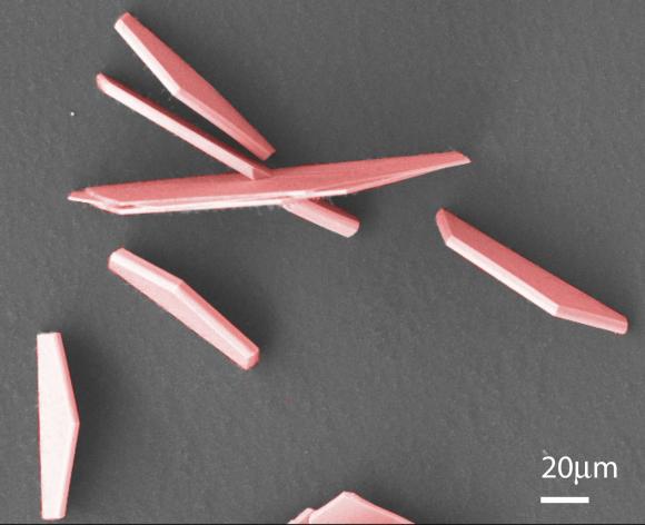
We report the synthesis of high-quality single-crystal two-dimensional, layered nanostructures of silicon telluride, Si2Te3, in multiple morphologies controlled by substrate temperature and Te seeding. Morphologies include nanoribbons formed by VLS growth from Te droplets, vertical hexagonal nanoplates through vapor–solid crystallographically oriented growth on amorphous oxide substrates, and flat hexagonal nanoplates formed through large-area VLS growth in liquid Te pools. We show the potential for doping through the choice of substrate and growth conditions. Vertical nanoplates grown on sapphire substrates, for example, can incorporate a uniform density of Al atoms from the substrate. We also show that the material may be modified after synthesis, including both mechanical exfoliation (reducing the thickness to as few as five layers) and intercalation of metal ions including Li+ and Mg2+, which suggests applications in energy storage materials. The material exhibits an intense red color corresponding to its strong and broad interband absorption extending from the red into the infrared. Si2Te3 enjoys chemical and processing compatibility with other silicon-based material including amorphous SiO2 but is very chemically sensitive to its environment, which suggests applications in silicon-based devices ranging from fully integrated thermoelectrics to optoelectronics to chemical sensors.

Monday, March 9, 2015

CVD Equipment Corp. and Penn State Partner on 2D ALD Research

As reported: CVD Equipment Corporation today announced that it will be entering into an industrial partnership with Penn State University.
 
CVD Equipment Corportion

Through the National Science Foundation’s Emerging Frontiers in Research and Innovation (EFRI) program, Penn State University (PSU) has been awarded $1.96M for Two-dimensional Atomic-layer Research and Engineering (2-DARE). This PSU project, headed by Professor Joan Redwing, will leverage CVD Equipment Corporation’s engineering and manufacturing capabilities to advance the deposition technologies and processes for producing novel 2D materials beyond graphene. The main focus will be on developing and optimizing the techniques for producing crystalline 2D transition metal dichalcogenides (TMDs) such as molybdenum disulfide (MoS2) and tungsten diselenide (WSe2). This work will pave the way for the future production of 2D materials, as they find their place in widespread industrial applications.

Joan Redwing

Prof. Joan Redwing, holds appointments in the Department of Electrical Engineering and the Department of Chemical Engineering at Penn State and is a member of the Materials Research Institute. Dr. Redwing’s research interests are in the general area of electronic materials synthesis and characterization with a specific emphasis on semiconductor thin film, nanowire and 2D materials fabrication by chemical vapor deposition.
 
Over recent years, the demonstration of graphene’s remarkable physical properties has led to the emerging application of graphene in many next generation products and devices. Although there is still much work to be done to fully understand graphene, many researchers have turned their attention to other 2D materials with equally promising and often unique properties. As such, a whole host of 2D materials are under vibrant interdisciplinary scientific study with an exciting outlook for disruptive technological advancements in big businesses such as semiconductor, optoelectronics, structural, and environmental applications, amongst others. Chemical vapor deposition and atomic layer deposition techniques are proving to be powerful for producing these atomically thin materials, but the often home-built university lab deposition equipment is limited in the process capabilities.

Tuesday, September 30, 2014

The National Science Foundation Funds Three Penn State Teams to Study Two-Dimensional Materials

 As reported by Newswise — Through the National Science Foundation’s Emerging Frontiers in Research and Innovation (EFRI) program, Penn State has been awarded $4 million over the next four years to lead two teams of investigators and support members of a third team in the new field of 2D crystals and layered materials.

A material that is only a single atomic-layer thick can have completely different properties than its bulk counterpart. A new field of nanoscale science and engineering is emerging to study the wide variety of two-dimensional materials and what happens when they are stacked one on top of the other. Potential applications include energy harvesting and storage, sensing, electronics and photonics, and bioengineering.

“There is a lot of interest in 2D materials beyond graphene, especially when considering stacking to form heterostructures because they can lead to phenomenal properties,” said Joshua Robinson, Corning Faculty Fellow of Materials Science and Engineering and associate director of Penn State’s Center for Two-dimensional and Layered Materials (2DLM). “I think we have a variety of excellent ideas in these novel materials, which is why we did so well with the EFRI.”
 
Crystalline large area WS2 have been grown directly on SiO2/Si substrates. The top left panel exhibits a high resolution transmission electron microscopy (HRTEM) image of the edge of a single-layer WS2 film. The top left panel depicts a schematic representation of the as grown WS2 film. A photograph of a WS2 film transferred onto a substrate is shown on the right panel, exhibiting the high contrast of the WS2 over SiO2/Si (films are cyan in color). (Picture from Ana Laura Elias, Penn State, Newswise)

The EFRI awards fund interdisciplinary teams of researchers in rapidly advancing fields of fundamental engineering research. The 2014 awards, called 2-DARE, for Two-dimensional Atomic-layer Research and Engineering, were awarded to nine teams in the U.S., three of which include Penn State researchers.

• “2D Crystal Formed by Activated Atomic Layer Deposition” is led by Joan Redwing, professor of materials science and engineering and electrical engineering, with co-PIs Ying Liu, Nasim Alem, Thomas Jackson and Suzanne Mohney, all faculty at Penn State. The award is for $1,964,494.

“Our project is aimed at developing Chemical Vapor Deposition (CVD) and Atomic Layer Deposition (ALD) processes to synthesize 2D materials. The 2D crystal films will be explored for applications in thin film electronics and superconductivity,” said Joan Redwing.

• "Ultra-low Power, Collective-state Device Technology Based on Electron Correlation in Two-Dimensional Atomic Layers" is led by Joshua Robinson with Co-PIs Suman Datta and Roman Engel-Herbert of Penn State, James Freericks, Georgetown University and Eva Andrei, Rutgers University. The award is for $2,000,000.

“This program will develop a ‘post silicon’ transistor based on the principal of strong electron correlation and associated phase transitions in two-dimensional materials,” said Robinson.

In addition, a third funded project, “Crystalline Atomically Thin Layers for Photonic Applications,” is a multidisciplinary collaboration between Rensselaer Polytechnic Institute, Penn State, Virginia Polytechnic Institute and State University, and Washington University in St. Louis investigating 2D material synthesis, condensed matter theory, and optical engineering, with the goal of developing a new class of photonic devices. Led by RPI, this $2,000,000 project includes Penn State co-PIs Zhiwen Liu, professor of electrical engineering, and research associate in physics Ana Laura Elias Arriaga. The Penn State subaward is $740,000.

“The goal of our project is to study the nonlinear optical properties of two-dimensional transition metal dichalcogenides and investigate their photonic applications. These 2D materials have very large optical nonlinearity, and, for example, can produce strong second harmonic generation. The combination of their novel optical properties and atomic thickness creates a unique opportunity for using these materials to ‘dress’ photonic devices and provide new functionalities,” Zhiwen Liu said.

“2D expertise is very diverse at Penn State and includes electronics, bio, optics, synthesis, characterization and theory,” said Mauricio Terrones, director of the 2DLM Center and professor of physics, chemistry and materials science and engineering. “Including students, post-docs and faculty, we have about 50 people involved.”

With recent publications in high impact journals,such as Nature Chemistry, Nature Communications, Nature Materials, Nano Letters and ACS Nano, Penn State researchers are taking a leading role in the exploration of 2D materials, Terrones said. Recently, the Department of Physics hired two new faculty members to complement the expertise already available, he added.

In addition to the National Science Foundation EFRI 2-DARE awards, 2DLM Center faculty have been successful with several other high profile awards from the Army, Air Force, and Defense Threat Reduction Agency and have recently put an emphasis on industry-driven research through a variety of industrial partnerships.

Wednesday, May 21, 2014

Hybrid technology for 2D electronics by graphene/molybdenum disulfide heterostructures grown by CVD

Nanotechweb.org reports that Researchers in the US have unveiled a new CMOS-compatible technology to integrate different two-dimensional materials into a single electronic device. The team, led by Tomás Palacios of the Massachusetts Institute of Technology, constructed large-scale electronic circuits based on graphene and molybdenum sulphide heterostructures grown by chemical vapour deposition where MoS2 was used as a transistor channel, and graphene as contact electrodes and circuit interconnects. The fabrication process itself might be extended to fabricate heterostructures from any type of 2D layered material with potential applications in flexible and transparent electronics, sensors, tunnelling FETs and high-electron mobility transistors.
 
Demonstration of a novel technology for constructing large-scale electronic systems based on graphene/molybdenum disulfide (MoS2) heterostructures grown by chemical vapor deposition.
 
Mor details on this work in the article below:
 
Lili Yu, Yi-Hsien Lee, Xi Ling, Elton J. G. Santos, Yong Cheol Shin , Yuxuan Lin, Madan Dubey, Efthimios Kaxiras, Jing Kong, Han Wang, and Tomás Palacios
Nano Lett., DOI: 10.1021/nl404795z Publication Date (Web): May 8, 2014

Abstract: Two-dimensional (2D) materials have generated great interest in the past few years as a new toolbox for electronics. This family of materials includes, among others, metallic graphene, semiconducting transition metal dichalcogenides (such as MoS2), and insulating boron nitride. These materials and their heterostructures offer excellent mechanical flexibility, optical transparency, and favorable transport properties for realizing electronic, sensing, and optical systems on arbitrary surfaces. In this paper, we demonstrate a novel technology for constructing large-scale electronic systems based on graphene/molybdenum disulfide (MoS2) heterostructures grown by chemical vapor deposition. We have fabricated high-performance devices and circuits based on this heterostructure, where MoS2 is used as the transistor channel and graphene as contact electrodes and circuit interconnects. We provide a systematic comparison of the graphene/MoS2 heterojunction contact to more traditional MoS2-metal junctions, as well as a theoretical investigation, using density functional theory, of the origin of the Schottky barrier height. The tunability of the graphene work function with electrostatic doping significantly improves the ohmic contact to MoS2. These high-performance large-scale devices and circuits based on this 2D heterostructure pave the way for practical flexible transparent electronics.

Sunday, May 4, 2014

Flexible monolayer circuit design by Vanderbilt and ORNL

Vanderbilt University reported - How to create nanowires only three atoms wide with an electron beam - "Junhao Lin, a Vanderbilt University Ph.D. student and visiting scientist at Oak Ridge National Laboratory (ORNL), has found a way to use a finely focused beam of electrons to create some of the smallest wires ever made. The flexible metallic wires are only three atoms wide: One thousandth the width of the microscopic wires used to connect the transistors in today’s integrated circuits."
 
“This will likely stimulate a huge research interest in monolayer circuit design,” Lin said. Because this technique uses electron irradiation, it can in principle be applicable to any kind of electron-based instrument, such as electron-beam lithography.”
 
One of the intriguing properties of monolayer circuitry is its toughness and flexibility. It is too early to predict what kinds of applications it will produce, but “If you let your imagination go, you can envision tablets and television displays that are as thin as a sheet of paper that you can roll up and stuff in your pocket or purse,” Pantelides commented.
 
In addition, Lin envisions that the new technique could make it possible to create three-dimensional circuits by stacking monolayers “like Lego blocks” and using electron beams to fabricate the wires that connect the stacked layers.
 
Full report from Vanderbilt University can be found here and please check out the video and the publication below for more insights!


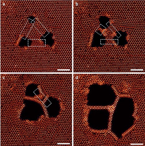
Series of still scanning electron micrographs (a to d) show how the electron beam is used to create nanowires. (Junhao Lin / Vanderbilt)


Junhao Lin, a Vanderbilt University Ph.D. student and visiting scientist at Oak Ridge National Laboratory (ORNL), has found a way to use a finely focused beam of electrons to create flexible metallic wires that are only three atoms wide: One thousandth the width of the microscopic wires used to connect the transistors in today's integrated circuits and some of the smallest wires ever made. The discovery gives a boost to efforts aimed at creating electrical circuits on monolayered materials, raising the possibility of flexible, paper-thin tablets and television displays. [youtube.com]

Atomic mechanism of the semiconducting-to-metallic phase transition in single-layered MoS2
Yung-Chang Lin, Dumitru O. Dumcenco, Ying-Sheng Huang & Kazu Suenaga        
Nature Nanotechnology (2014) doi:10.1038/nnano.2014.64 Published online 20 April 2014
 
Abstract:
Phase transitions can be used to alter the properties of a material without adding any additional atoms and are therefore of significant technological value. In a solid, phase transitions involve collective atomic displacements, but such atomic processes have so far only been investigated using macroscopic approaches. Here, we show that in situ scanning transmission electron microscopy can be used to follow the structural transformation between semiconducting (2H) and metallic (1T) phases in single-layered MoS2, with atomic resolution. The 2H/1T phase transition involves gliding atomic planes of sulphur and/or molybdenum and requires an intermediate phase (α-phase) as a precursor. The migration of two kinds of boundaries (β- and γ-boundaries) is also found to be responsible for the growth of the second phase. Furthermore, we show that areas of the 1T phase can be controllably grown in a layer of the 2H phase using an electron beam.
 

Friday, April 18, 2014

Growth and stacking 2D materials MoS2, WSe2, and hBN on epitaxial graphene by CVD

Researchers at Penn State's Center for 2-Dimensional and Layered Materials and the University of Texas at Dallas have shown the ability to grow high quality, single-layer materials one on top of the other using CVD (chemical vapor deposition). Furthermore, they have demonstrated growth and stacking 2D materials MoS2, WSe2, and hBN on epitaxial graphene by CVD.  

 
The stacking of two-dimensional layered materials: MoS2, WSe2, and hBN on epitaxial graphene (Picture from graphical abstract:ACS Nano, DOI: 10.1021/nn5003858)
 
 
Read more at Nanowerk: Making new materials an atomic layer at a time or in the publication below.
Direct Synthesis of van der Waals Solids

Yu-Chuan Lin, Ning Lu, Nestor Perea-Lopez, Jie Li, Zhong Lin, Xin Peng, Chia Hui Lee, Ce Sun, Lazaro Calderin, Paul N. Browning, Michael S. Bresnehan, Moon J. Kim, Theresa S. Mayer, Mauricio Terrones , and Joshua A. Robinson

ACS Nano, Article ASAP, DOI: 10.1021/nn5003858, Publication Date (Web): March 18, 2014

Abstract:
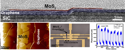
The stacking of two-dimensional layered materials, such as semiconducting transition metal dichalcogenides (TMDs), insulating hexagonal boron nitride (hBN), and semimetallic graphene, has been theorized to produce tunable electronic and optoelectronic properties. Here we demonstrate the direct growth of MoS2, WSe2, and hBN on epitaxial graphene to form large-area van der Waals heterostructures. We reveal that the properties of the underlying graphene dictate properties of the heterostructures, where strain, wrinkling, and defects on the surface of graphene act as nucleation centers for lateral growth of the overlayer. Additionally, we show that the direct synthesis of TMDs on epitaxial graphene exhibits atomically sharp interfaces. Finally, we demonstrate that direct growth of MoS2 on epitaxial graphene can lead to a 103 improvement in photoresponse compared to MoS2 alone.


A photosensor fabricated on the MoS2/graphene heterostructure. (Image: Yu-Chuan Lin, Penn State)

Tuesday, April 8, 2014

One-Atom-Thick Layers of Molybdenum Diselenide by CVD

Azonano.com reports today on a "Novel Scalable Method for Producing One-Atom-Thick Layers of Molybdenum Diselenide" published by Rice University USA and Nanyang Technological University in Singapore. A scalable method for making one-atom-thick layers of molybdenum diselenide. The results are also reported in a press release by Rice University including downloads to released material.
  • MoS2 is a  semiconductor that is similar to graphene but has better properties
  • Can be integrated for future switchable transistors and light-emitting diodes
  • The two-dimensional molybdenum diselenide was made by chemical vapor deposition (CVD)


A TEM image that shows the individual atoms in a two-dimensional sheet of molybdenum diselenide (Azonano.com) 

“This new method will allow us to exploit the properties of molybdenum diselenide in a number of applications,” said study leader Pulickel Ajayan, chair of Rice’s Department of Materials Science and NanoEngineering. “Unlike graphene, which can now easily be made in large sheets, many interesting 2-D materials remain difficult to synthesize. Now that we have a stable, efficient way to produce 2-D molybdenum diselenide, we are planning to expand this robust procedure to other 2-D materials.”

Full store here: http://www.azonano.com/news.aspx?newsID=29848 and the publication in ACS Nano Letters below:

Band Gap Engineering and Layer-by-Layer Mapping of Selenium-Doped Molybdenum Disulfide

Yongji Gong, Zheng Liu, Andrew R. Lupini, Gang Shi, Junhao Lin, Sina Najmaei, Zhong Lin, Ana Laura Elías, Ayse Berkdemir, Ge You, Humberto Terrones, Mauricio Terrones, Robert Vajtai, Sokrates T. Pantelides, Stephen J. Pennycook, Jun Lou, Wu Zhou, and Pulickel M. Ajayan

Nano Lett., 2014, 14 (2), pp 442–449, DOI: 10.1021/nl4032296


Abstract: Ternary two-dimensional dichalcogenide alloys exhibit compositionally modulated electronic structure, and hence, control of dopant concentration within each individual layer of these compounds provides a powerful tool to efficiently modify their physical and chemical properties. The main challenge arises when quantifying and locating the dopant atoms within each layer in order to better understand and fine-tune the desired properties. Here we report the synthesis of molybdenum disulfide substitutionally doped with a broad range of selenium concentrations, resulting in over 10% optical band gap modulations in atomic layers. Chemical analysis using Z-contrast imaging provides direct maps of the dopant atom distribution in individual MoS2 layers and hence a measure of the local optical band gaps. Furthermore, in a bilayer structure, the dopant distribution is imaged layer-by-layer. This work demonstrates that each layer in the bilayer system contains similar local Se concentrations, randomly distributed, providing new insights into the growth mechanism and alloying behavior in two-dimensional dichalcogenide atomic layers. The results show that growth of uniform, ternary, two-dimensional dichalcogenide alloy films with tunable electronic properties is feasible.