Monday, April 24, 2023
Oxford Instruments to supply KAUST with hardware upgrades and ALE systems
Wednesday, April 19, 2023
Call for Papers on ALD & ALE Applications, at ECS Fall Meeting / Gothenburg Oct. 2023 ►►DEADLINE EXPIRES APRIL 21◄◄
The Electrochemical Society (ECS) conference is an international event running every spring and fall, and gathering 2000-4000 participants and 30-40 exhibitors both from academia and industry.
The conference has a strong focus on emerging technology and applications in both electrochemistry and solid-state science & technology.
This fall the event will be held as 244th ECS Meeting on Oct. 8-12, 2023 in Gothenburg (Sweden).
The full program as well as information on travel assistance for students can be found on https://www.electrochem.org/
The organizers of symposium G01 on “Atomic Layer Deposition & Etching Applications, 19” encourage you to submit your abstracts on the following (and closely related) topics:
1. Semiconductor CMOS applications: development and integration of ALD high-k oxides and metal electrodes with conventional and high-mobility channel materials;
2. Volatile and non-volatile memory applications: extendibility, Flash, MIM, MIS, RF capacitors, etc.;
3. Interconnects and contacts: integration of ALD films with Cu and low-k materials;
4. Fundamentals of ALD processing: reaction mechanisms, in-situ measurement, modeling, theory;
5. New precursors and delivery systems;
6. Optical and photonic applications;
7. Coating of nanoporous materials by ALD;
8. MLD and hybrid ALD/MLD;
9. ALD for energy conversion applications such as fuel cells, photovoltaics, etc.;
10. ALD for energy storage applications;
11. Productivity enhancement, scale-up and commercialization of ALD equipment and processes for rigid and flexible substrates, including roll-to-roll deposition;
12. Area-selective ALD;
13. Atomic Layer Etching (‘reverse ALD’) and related topics aiming at self-limited etching, such as atomic layer cleaning, etc.
Abstract submission
Meeting abstracts should be submitted not later than the deadline of April 21, 2023 via the ECS website: Abstract submission instruction
List of invited speakers
· Johan Swerts, (Imec, Belgium) KEYNOTE: ALD challenges and opportunities in the light of future trends in electronics
· Stephan Wege (Plasway Technology, Germany), Reactor design for combined ALD & ALE
· Masanobu Honda (TEL, Japan), Novel surface reactions in low-temperature plasma etching
· Barbara Hughes, (Forge Nano, USA), Dual Coatings, Triple the Benefit; Atomic Armor for Better Battery Performance
· Juhani Taskinen, (Applied Materials-Picosun, Finland), ALD for biomedicine
· Alex Kozen (Univ. of Maryland, USA), ALD for improved Lithium Ion Batteries
· Malachi Noked (Bar-Ilan Univ., Israel), ALD/MLD for batteries
· Yong Qin (Chinese Academy of Sciences), ALD for catalysis
· Jan Macák, (Univ. of Pardubice, Czechia), ALD on nanotubular materials and applications
· Bora Karasulu, Univ. of Warwick, UK), Atomistic Insights into Continuous and Area-Selective ALD Processes: First-principles Simulations of the Underpinning Surface Chemistry
· Ageeth Bol (Univ. Michigan, USA), ALD on 2D materials
· Pieter-Jan Wyndaele (KU Leuven-imec, Belgium), Enabling high-quality dielectric passivation on Monolayer WS2 using a sacrificial Graphene Oxide template
· Elton Graugnard (Boise State Univ., USA), Atomic Layer Processing of MoS2
· Han-Bo-Ram Lee (Incheon National Univ., Korea), Area-Selective Deposition using Homometallic Precursor Inhibitors
· Ralf Tonner (Univ. Leipzig, Germany), Ab initio approaches to area-selective deposition
· Nick Chittock (TU Eindhoven, Netherlands), Utilizing plasmas for isotropic Atomic Layer Etching
· Heeyeop Chae (Sungkyunkwan Univ., Korea), Plasma-enhanced Atomic Layer Etching for Metals and Dielectric Materials
· Charles Winter (Wayne State Univ., USA), New Precursors and Processes for the Thermal ALD of Metal Thin Films
· Anjana Devi, Ruhr Univ. Bochum, Germany), Novel precursors dedicated for Atomic Layer Processing
Visa and travel
For more information, see: www.electrochem.org/244/visa-
In addition, Mrs. Francesca Spagnuolo at the ECS (Francesca.Spagnuolo@
We are looking forward to meeting you in Gothenburg !
Monday, April 10, 2023
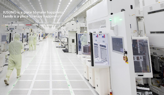
Korea’s Jusung Engineering set to supply non-memory chip gears overseas
“The test conducted by our global customer on the Guidance Series, an ALD equipment developed for the first time in the world in 2020, has been completed and we expect the purchase order to come in the first half of this year,” Hwang told Maeil Business Newspaper.


%20(1).png)


