Tuesday, January 31, 2017

Meaglow from Canada to exhibit Hollow Cathode Plasma ALD at EuroCVD/Baltic ALD 2017

We are very happy to have a Candian company exhibiting at the joint EuroCVD-Baltic ALD 2017 conference in Sweden. Pleas hurry up to book your exhibition table since we have only 9 left and we will most probably sell out theexhibition.


Since 2009, Meaglow has been manufacturing crystal growth research reactors and supplying Hollow Cathode Plasma Sources to upgrade ALD, MOCVD, MBE, and other custom systems. Notable achievements include growing yellow InGaN thin films in the green gap, featured in Compound Semiconductor, and Semiconductor Today. 

Meaglow was founded by Scott Butcher, with over 20 years of nitride semiconductor experience, more than 100 referred journal and conference papers published, Dr. Butcher is an expert and pioneer in the industry. Holding eight patent families globally and being involved in three prior start up companies in addition to Meaglow Scott’s prior technologies have attracted over $20 million in funding to bring multiple thin film systems to market

Meaglow is well known in the ALD community for a range of hollow cathode (HC) plasma sources that they offer for PEALD.


Hollow cathode (HC) plasma sources, are an alternative to ICP and CCP sources. They’ve been around for quite a number of years and have been adopted for cathodic sputtering in PV systems, but past designs have been overly complicated for many PECVD applications involving the traditional material sets.(meaglow.com).

Monday, January 30, 2017

Hitachi High-Technologies and Picosun Oy launch a collaboration in Plasma-enhanced ALD

Tokyo, Japan and Espoo, Finland - 30 January 2017 - Hitachi High-Technologies Corporation (TSE:8036, Hitachi High-Tech) and Picosun Oy announce a revolutionary technological co-operation in plasma-enhanced atomic layer deposition (PE-ALD). The aim of this co-operation is to bring thin film coating technologies to a completely new level. Hitachi High-Tech’s and Picosun’s joint breakthrough, the novel Microwave Electron Cyclotron Resonance (ECR) ALD technology will disrupt all advanced semiconductor industries. 
 

Promotion Video: MECRALD - novel, revolutionary plasma-enhanced ALD technology By Hitachi High-Technologies and Picosun. (youtube.com)

 
In the PE-ALD reactor, Hitachi High-Tech’s powerful ECR plasma generator is integrated with Picosun’s industry-proven, digitally controlled ALD system. Consequently, the quality of the deposited materials is substantially better, and the deposition process is much more precise than existing traditional ALD and plasma-enhanced ALD methods.

Some superior results for various nitride and oxide films have been confirmed with 300 mm semiconductor wafers so far and some other process applications are under evaluation.

About Hitachi High-Technologies Corporation

Hitachi High-Technologies Corporation, headquartered in Tokyo, Japan, is engaged in activities in a broad range of fields, including Science & Medical Systems, Electronic Device Systems, Industrial Systems, and Advanced Industrial Products. The company's consolidated sales for FY 2015 were approx. 629 billion [USD5.8 billion]. For further information, visit http://www.hitachi-hightech.com/global/.

About Picosun Oy

Picosun provides the most advanced ALD thin film coating technology to enable the industrial leap into the future, with turn-key production solutions and unmatched expertise in the field. Today, PICOSUN™ ALD equipment are in daily manufacturing use in numerous major industries around the world. Picosun is based in Finland, with subsidiaries in North America, Singapore, Taiwan, China, and Japan, and a world-wide sales and support network. For more information visit www.picosun.com. 


Friday, January 27, 2017

Atomic Scale Processing Workshop 4 April 2017 with CEA_Leti MINATEC

Atomic Scale Processing Workshop 4 April 2017 at CEA/Leti & MINATEC, Grenoble, France.  Sign up for FREE


Description

The aim of this one-day workshop is to give an overview of current topics in the field of atomic scale processing for a range of applications. It is open to scientists and technologists working in industry and academia, with an interest in recent progress plus future trends in research and development.

- Participation is free but registration is mandatory.
- Lunch and refreshments are included
- Topics
  • Atomic layer etch (ALE): a precision technique to enable tomorrow’s technology
  • Latest advances and new technologies for atomic scale process applications
  • Ion beam developments in etch and deposition
  • ALD and 2D overview: technology and results
  • Ion beam research results at LETI
...And more topics to be announced

Apple Dual Fold-Out/Fold-In Form Factor phone

As reported today by Petently Apple, Apple's Third Major Folding iPhone Invention has come to Light Illustrating a Dual Fold-Out/Fold-In Form Factor.


Earlier Patently Apple also reported that Samsung continues to internally debate whether to launch a Fold-Out Smartphone later this year (LINK).


Thursday, January 26, 2017

Entegris seeking ALD/CVD precursor synthetic chemist in Austin

Seeking an experienced organometallic synthetic chemist handling air, moisture and thermally sensitive compounds for thin film ALD/CVD precursor development. Join the fastest growing BU in the company! https://lnkd.in/egAdKQT

Vital Control in Fab Materials Supply-Chains

Vital Control in Fab Materials Supply-Chains: The inaugural Critical Materials Council (CMC) Conference, co-sponsored by Solid State Technology, happened May 5-6 in Hillsboro, Oregon. Held just after the yearly private CMC meeting, the public CMC Conference provides a forum for the pre-competitive exchange of information to control the supply-chain of critical materials needed to run high-volume manufacturing (HVM) in IC fabs. The next CMC Conference will happen May 11-12 in Dallas, Texas.


John Smythe, Distinguished Member of Technical Staff of Micron Technology, explains approaches to controlling materials all the way to point-of-use. (Source: TECHCET CA)

At the end of the 2016 conference, a panel discussion moderated by Ed Korczynski was recorded and transcribed. The following is an edited excerpt of the conversation between the following industry experts:
  • Jean-Marc Girard, CTO and Director of R&D, Air Liquide Advanced Materials,
  • Jonas Sundqvist, Sr. Scientist, Fraunhofer IKTS; and co-chair of ALD Conference, and
  • John Smythe, Distinguished Member of Technical Staff, Micron Technology
Please visit Semiconductor Manufacturing and Design (SemiMD.com) published by Extension Media for the full article by Ed Korczynski, Sr. Technical Editor.


Jonas Sundqvist, Sr. Scientist of Fraunhofer IKTS, discusses collaboration with industry on application-specific ALD R&D. (Source: TECHCET CA)


Tack så mycket CVD & ALD2017 Folks - Abstract submission is now closed and >200 Abstracts are now in review!

Tack så mycket CVD & ALD2017 Folks - Abstract submission is now closed and >200 Abstracts are now in review!

Please visit eurocvd-balticald2017.se for the latest information and support to plan your participation in EuroCVD / Baltic ALD 2017. 

There are still some nice sponsoring alternatives open and the exhibition also have a few places left - It will be sold out!


Review of EFDS Workshop – ALD for Industry 2017


Text and Photos as Posted on


After half a day of tutorials on ALD thechnology and fundamentals and a nice get-together at the Freiberger Schankhaus in Dresden in the evening, we heard great talks about the broad range of ALD processes, ALD application and ALD equipment in the great ambiance of the Swissôtel Dresden.


Platin Sponsors:
logo_air-liquide  logo_asm
logo_beneq  logo_fhr
logo_picosun

Gold Sponsors:

logo_cs-clean logo_ebera logo_euris logo_lesker logo_modularflow logo_sentech logo_pegasus logo_rasirc logo_strem-chemicals logo_ultratech-cnt

Lam Research doubled install base of ALE in Logic 2016

Lam Research just presented their 4Q/2016 earnings. 2016 was the fifth consecutive year of growth and outperformance for Lam with a shipments CAGR of almost 20% over that period and shipments grew to a record $6.7 billion. As an example of the success 3D NAND shipments grew by over 80% in 2016, almost twice the rate of growth in NAND’s WFE. Please find all detailas in the Seeking Alpha Earings Call Transcript here

With respect to new existing atomic level control technology Lam has strengthened its momentum in foundry and logic with significant application share gains from the 2016 nodes to the 10 and 7 nanometer nodes. As an example, during the quarter they more than doubled their install base for  Atomic Layer Etch (ALE) system for logic self-aligned contact application with their dielectric etch product and mixed mode pulsing technology.

Seeking Alpha Earings Lam Research Call Slides here.

Wednesday, January 25, 2017

The NaMLab Novel High k Application Workshop 2017 in Dresden

NaMLab invites to the Novel High-k Application Workshop on March 9th and 10th, 2017. New challenges offered by the application of high-k dielectric materials in micro– and nanoelectronics will be discussed by more than 80 participants from industry, research institutes and universities. One main focus will be on the ferroelectric properties of HfO2. 

 
NaMLab created with the workshop a stimulating platform for application-oriented scientist to exchange ideas and discuss latest experimental results on MIM-capacitors, process technology, leakage & reliability as well as characterization of high-k dielectrics integrated in silicon based micro– and nanoelectronics. The ferroelectric properties of doped HfO2 and ZrO2 were discovered 10 years ago. On the second day of the workshop, root causes for the formation of this so far unknown phase will be discussed.

Registration for the workshop started:
- registration rate: participants: 12€/day  - students: 10€/day  (includes all meals and coffee breaks)
- registration rate can be paid by credit card, pay pal (Europe only: direct transfer)


Preliminary agenda:    March 9th  to 10th
Workshop location: Max Planck Institute PKS (Physics of Complex Systems), Noethnitzer Strasse 38

Sponsors:
  http://www.oxford-instruments.com/  
   http://www.strem.com/
  http://globalfoundries.com/

Co-organized by:

Functional Perovskites by Atomic Layer Deposition – An Overview

Here is a fresh review on perovskites (thanks for sharing Henrik Pedersen) by ALD from the Group of Prof. Nilsen at Oslo University, which as far as I know are the true masters of creating and understanding complex multi component metal oxides by ALD. I like that the review starts by placing the topic of perovskites in a historical context "In the 90 years since Victor Goldschmidt properly described the perovskite structure in his inaugural paper “Die Gesetze der Krystallochemie”, it has become one of the most studied and iconic classes of materials".


[Wikipedia] Victor Moritz Goldschmidt (Zürich, January 27, 1888 – March 20, 1947, Oslo) was a mineralogist considered (together with Vladimir Vernadsky) to be the founder of modern geochemistry and crystal chemistry, developer of the Goldschmidt Classification of elements. (photo from Wikipedia)

Functional Perovskites by Atomic Layer Deposition – An Overview 

Henrik Hovde Sønsteby*, Helmer Fjellvåg and Ola Nilsen
Adv. Mater. Interfaces 2017, 1600903


 Preview article


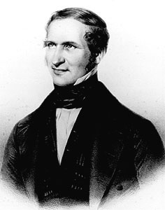
Gustav Rose who discovered the mineral perovskite

The mineral perovskite composed of calcium titanate (CaTiO3) was discovered in the Ural Mountains of Russia by Gustav Rose form The Kindom of Prussia in 1839 and is named after Russian mineralogist Lev Perovski (1792–1856). Amongst others, Gustav Rose studied under famous Swedish physical chemist Jöns Jakob Berzelius (1779–1848) in Stockholm. Berzelius is considered, along with Robert Boyle, John Dalton, and Antoine Lavoisier, to be one of the founders of modern chemistry and introduced chemical notation. [Wikipedia]

Jöns Jacob Berzelius (1779–1848) [Wikipedia]


Monday, January 23, 2017

KAUST technology extracts more from wastewater using ALD catalyst

KAUST present a novel electrocatalytic and microfiltration polymeric hollow fiber using ALD of platinum that is fabricated for simultaneous recovery of energy (H2) and clean fresh water from wastewater, hence addressing two grand challenges facing society in the current century (i.e., providing adequate supplies of clean fresh water and energy as the world's population increases).


More information: Krishna P. Katuri et al. A Microfiltration Polymer-Based Hollow-Fiber Cathode as a Promising Advanced Material for Simultaneous Recovery of Energy and Water, Advanced Materials (2016). DOI: 10.1002/adma.201603074

Read more at: https://phys.org/news/2017-01-wastewater.html#jCp
The results have been published in Adv. Mater., DOI: 10.1002/adma.201603074 and according to the supporting information the catalyst deposition by ALD on the outer surface of a POD hollow fiber membranes and was carried out on Oxford Instrument ALD system FlexAL

Read more at: https://phys.org/news/2017-01-wastewater.html#jCp

Fresh water scarcity and energy security are two critical global challenges facing us today. Researchers at KAUST have now created an advanced material that can address both problems simultaneously by producing clean water and hydrogen from wastewater.

Wednesday, January 18, 2017

Candadian researchers introduce novel ceramic ALD coated solid electrolyte for safe Li-batteries

Candadian researchers from University of Calgary report novel ceramic ALD coated solid electrolyte for safe Li-batteries (LINK): Existing lithium-ion batteries like those used in the Tesla Motors cars, Chevrolet Volt, Nissan Leaf and other electric and plug-in hybrid vehicles, as well as in portable electronics, use membranes of organic polymer compounds and lithium salts as the electrolyte. 
 
This is an illustration of a Li-rich garnet structure based all-solid-state-Li battery. While other research groups in the world have used garnet to build lithium batteries, “We showed we can use the lithium metal very efficiently, with the lowest interface-charge transfer resistance between the lithium electrode and the garnet electrolyte,” Thangadurai says. (Figure from www.ucalgary.ca)

The electrolyte in a battery separates the two electrodes (the positive cathode and the negative anode), and conducts the lithium ions between the electrodes during charging and discharging cycles. Currently used organic polymer-based electrolytes are flammable, so fire is a safety issue.

Instead of organic polymers for their battery, Wachsman and co-principal investigators Thangadurai and Liangbing Hu (at the UMD), along with other UMD scientists, used a solid ceramic electrolyte, which doesn’t burn.

The research team also used, for the first time, a technique called atomic layer deposition to place a thin film of aluminum oxide on top of a garnet structure coating the ceramic electrolyte.
 

Tuesday, January 17, 2017

2nd Area Selective Deposition workshop (ASD 2017), April 20-21, 2017

In collaboration with COST action HERALD, Eindhoven University will host the 2nd Area Selective Deposition workshop (ASD 2017), which will be held on April 20-21, 2017. The aim of this workshop is to bring together leading scientists and engineers from both academia and industry, to discuss the fundamentals of area selective deposition, as well as its applications.

Similar to last year’s successful workshop at IMEC, ASD 2017 will consist of one day of presentations and discussions. This scientific program will take place on April 21 in the city center of Eindhoven (90 minutes from Amsterdam), and will be preceded by a welcome reception at Eindhoven University on April 20. We are pleased to confirm the following invited speakers: Stacey Bent (Stanford University), John Abelson (University of Illinois at Urbana-Champaign), Rong Chen (Huazhong University), and Younghee Lee (University of Colorado at Boulder).

In addition to several invited presentations, this year’s program will include a few contributed presentations to feature recent developments in the field. The topics for these presentations will be selected based on abstracts received. Furthermore, there will be a poster session covering work related to nucleation, selective deposition, and nanopatterning. The abstract deadline is February 21. Note that this deadline is relatively tight.

The workshop is free, but registration for the scientific program and the welcome reception is mandatory. The registration deadline is April 12. Please see www.nanomanufacturing.nl/ASD2017 for more information about abstract submission and registration.

The ASD Program Committee is looking forward to your attendance.

Scott Clendenning (Intel Corporation), Annelies Delabie (IMEC), Dennis Hausmann (LAM Research), Rami Hourani (Intel Corporation), Gregory Parsons (North Carolina State University), and Adrie Mackus (Eindhoven University of Technology)


COST Action MP1402 - HERALD
Hooking together European research in Atomic Layer Deposition

Monday, January 16, 2017

Encapsulix SAS selected as supplier of ALD-TFE deposition systems by leading Asian AMOLED manufacturer

January 16, 2017 : Encapsulix SAS today announced that it has been selected as the supplier of ALD-TFE deposition systems by a leading Asian AMOLED manufacturer. The first tool is presently under construction and scheduled for operation from the spring of 2017 onwards. The systems will be used to encapsulate flexible AMOLED displays with multifunctional nanolaminated coatings. The order was awarded to Encapsulix SAS after an extensive evaluation of available ALD equipment suppliers of barrier and encapsulation coatings.

The Infinity ALD equipment platform has the unique capability to deposit the most advanced nano-engineered coatings in a manufacturing environment. These coating have an overall thickness in the 20-50nm range, and typically comprise tens of sublayers of up to 10 different materials with thicknesses in the nanometer range. A wide range of available materials includes both inorganic (e.g. Al2O3, SiO2, ZrO2, TiO2, SiNx, HfO2,..) and organic (Alucone, Zircone, ..) nanolayers allowing to engineer the barrier, mechanical, optical en electrical properties at the atomic scale.

« This order confirms the technological superiority and leading Cost-Of-Ownership of our ALD-TFE equipment and process solutions for AMOLED manufacturing » stated Dr. Jacques Kools, founder and CEO of Encapsulix SAS. He also stated « We are now seeing rapid market adaptation of Nanolaminated ALD-TFE as the ideal solution for the emerging application of foldable OLED devices. »

About Encapsulix, Encapsulix was founded to address the geometric scaling of critical deposition requirements for industrial & microelectronic devices and foils. The company has its development and headquarters in Simiane- Collongue France, equipment development, sales and service in the USA. 
For more information:
Contact: www.encapsulix.com

For those of you attending ALD For Industry in Dresden 17-18 of January you will have an excellent opportunity to listen and be enlightened by Dr. Kools himself giving a talk entitled "Industrial deployment of nano-engineered ultrabarriers for encapsulation of organic electronic".

MAM2017 Conference: March 26-29, 2017 in Dresden

Starting with refractory metals and silicides in the 80's, moving to materials for advanced metallization in 1995, the MAM addresses new and challenging topics in the field of BEOL solutions, novelties in alternative interconnect systems and more widely advanced materials and structures relevant to micro and nano-electronics. Topics include both fundamental and applied research, as well as issues related to introduction into manufacturing. The 2017 conference from March 26 to March 29, 2017 also aims to address new challenges in the fields of Materials for Flexible Electronics, Nanodevices and Process and Device Modelling and Simulation.


MAM2017 Conference: March 26-29, 2017 

Web: LINK

Location
This year’s conference will be held in the city center of Dresden, Germany. The "Florence on the Elbe" is the capital of Saxony and located in the east of Germany. Dresden combines history, art, culture, architecture, industry and modern science:
The Frauenkirche and the Old Masters, the Blue Wonder and the Green Vault; the picturesque banks of the Elbe river and the popular Wilhelminian district; the baroque Old Town and the modern city center are just a few examples of the city`s world famous sights.

Abstracts due: 20th January 2017 (Abstracts 1/2 page (text only) or 1 page (incl. figures) to be submitted at www.mam-conf.org; Accepted abstracts to be distributed on memory stick at conference)
Paper acceptance: 27th January 2017
Early registration deadline: 20th February 2017
Submission of full length papers: April 15th 2017 (will be published in a special issue of Microelectronic Engineering) 
 

Sunday, January 15, 2017

Intermolecular enhances ferroelectricity in dopant-free ALD hafnium oxide

In a new paper published in Applied Physics Letters, Intermolecular discusses how it has developed a method for improving the ferroelectric properties of pure ALD hafnium oxide without introducing additional dopants. [Intermolecular, LinkedIn]
Ferroelectric hafnium oxide (HfO2) is being used in development for non-volatile memory applications, In front end by a ferroelectric MIS-FET and in backend by a MIM Capacitor integration. Since HfO2 is a standard material in both DRAM and Logic since 10 years or more the deposition method, tools an precursors for depositing ultra-thin layers by atomic layer deposition (ALD) are available and therefore very attractive choice as compared to more exotic materials (Sr, Ba) or previous PZT based ferroelectrics.

In previous studies, mixing hafnium and zirconium oxide together, doping the HfO2 with other elements, like silicon, aluminum, yttrium, strontium, lanthanum, and gadolinium, have been used to induce ferroelectricity in HfO2.
Now however, Intermolecular present new results (see below) were they by controlling the oxidant dose can promote ferroelectricity in dopant-free ALD hafnium oxide films. They were able to com near to total suppression of the monoclinic phase in sub-10 nm hafnium oxide films and obsreve a remanent polarization of 13.5 μC/cm2 in a 6.9 nm-thick hafnium oxide film. 
This is a similar high-k film thickness that is used in DRAM and embedded DRAM MIM Caps and also about the sam thickness that Globalfoundries, NaMLab and Fraunhofer have reported for their 28 nm FEFET NVM cells.