RASIRC Presents Novel Source for Oxidation and Nitridation for Atomic Layer Deposition
Describes anhydrous hydrazine and hydrogen peroxide surface functionalization and passivation
San Diego, Calif – May 31, 2016 –RASIRC today announced that Chief Technology Officer Dan Alvarez, PhD will present today Novel Oxidants and Sources of Nitrogen for Atomic Layer Deposition at the 229th Electrochemical Society Conference. The conference, held May 29-June 2, 2016 in San Diego, California, is a forum for sharing the latest scientific and technical developments in electrochemistry and solid state science and technology.
The RASIRC presentation describes how development of novel metal precursors for atomic layer deposition (ALD) has been driven by the need for improved high-K materials and low temperature deposition for metal nitride films. These metal precursors in turn require novel oxidant and nitrogen sources that are more reactive than water and ammonia but less aggressive than ozone and plasma methods. Alvarez will present data on how anhydrous hydrogen peroxide and anhydrous hydrazine have shown feasibility in ALD.
“The challenge for using anhydrous hydrogen peroxide and anhydrous hydrazine in commercial application has been that they are both difficult to deliver safely in a consistent and stable concentration,” said Alvarez. “RASIRC has developed and tested a method that overcomes these problems, making it practical for industry to use these reactive chemicals with new materials in ALD.”
The RASIRC formulation for delivery of highly reactive chemicals uses an inert organic solvent and membrane delivery system that delivers anhydrous gas from liquid sources. This maintains precursor vapor pressure at levels viable for ALD and raises the solution flash point, reducing risk of explosion. The RASIRC presentation will share results from experiments focused on SiGe(110) surface nucleation by anhydrous hydrogen peroxide
Here is a very interesting article "Event scans silicon road map, IoT as driver" by Rick Merritt in EETimes from Imec Tech Forum that took place this week in Brussels. ALD, EUV and Gate All Around Nanowire transistors is still all on the table.
As previous years Imec also this year rewarded "The imec lifetime of innovation award 2016" and this year it was given to Dr. Gordon Moore himself. Below is an interview with Gordon Moore in Hawaii made by Luc Van den Hove - President & CEO of imec.
Interview with Dr. Gordon Moore who was granted the imec lifetime of innovation award 2016. Interview by Luc Van den Hove - President & CEO of imec. [www.youtube.com]
Ivo Raaijmakers, chief technologist of equipment maker ASM International on scaling
“The industry will find a way to continue scaling, not a classic Denard scaling, but there are many innovations in the pipeline…so maybe the growth rate will decrease a bit and the cadence of new nodes will decrease…but we don’t see this as a downward spiral, just a shift from nodes maybe every three years instead of two,”
An Steegen, the senior vice president of process technology at Imec on EUV and the 5 and 3 nm nodes
“We make daily progress [on EUV]…the most complex layers at the back end where it is very difficult for immersion will be the first insertion point and the sooner the better,” said An Steegen, the senior vice president of process technology at Imec.
Rick Merritt in EETimes reports that: Steegen believes horizontal nanowires, a sort of gate-all-around deisgn, will be the next big transisitor. They could be stacked laterally to deliver 30-50% gains in lower power and higher performance, she said. Imec is still evaluating first-generation designs that it will need to prove out in second-gen hardware.
“We aways need new features to manage power density, we had dynamic frequency and voltage scaling a few years ago, FinFETs now and I believe nanowires in the future,” Steegen said.
Further out vertical nanowires could be a next step. However “going vertical is very disruptive” and these transistors cannot be stacked without area penalties, potentially forcing a move to new high-mobility III-V materials to hit performance targets, she said.
Imec is exploring lateral and vertical nanowires as successors to the FinFET. (Image: Imec)
HERALD COST Action & the ISSON16 co-organize a Training School on Atomic Layer Deposition on 2-4 July 2016 July 2016, at Thessaloniki, Greece.
Six (6) students will be granted by HERALD COST Action with 650 € to participate to the lectures of the ALD Training School and ISSON16. E-mail your application to Dr. Spyros Kassavetis (skasa@physics.auth.gr). The program will be announced soon.
Deadline for applications: 5th of June 2016 .
The granted students can submit abstract and participate to NANOTEXNOLOGY 2016 Conferences under a special registration fee. The deadline for abstract submission is 5th of June 2015. For more information, you can visit our NANOTEXNOLOGY 2016 website.
ESPOO, Finland, 26th May, 2016 – Picosun Oy, the leading supplier of high quality ALD (Atomic Layer Deposition) production solutions, brings to the printed electronics market ALD equipment specifically designed for large area flexible electronics encapsulation.
Manufacturing electronic components on flexible plastic substrates enables light-weight, bendable, and lower cost end-user products. Flexible displays, wearable electronics and “smart” clothes are some of the most common examples. More specific applications can be found in medical and security industries, where advanced X-ray detectors are being developed utilizing organic electronic components printed on plastic foils.
Organic electronics has the potential to enable a whole new generation of products, but one of its main drawbacks is the components’ sensitivity to moisture and airborne impurities. Ultra-thin ALD nanolaminates provide an ideal solution to this. Flexible, invisible, and practically weightless ALD films form dense and pinhole-free encapsulation over the components’ surface, down to the smallest nanoscale details. In Picosun’s new large area ALD tools, especially developed for the needs of the printed electronics industries, high quality ALD films can be manufactured cost-efficiently on large plastic sheets and at temperatures low enough for sensitive organic materials.
“We have again put our extensive expertise in ALD system design to work to realize completely novel technology for the vast market of printed electronics. Our new, large area batch ALD systems are developed and optimized in collaboration with these industries. Their disruptive design enables cost-efficient encapsulation of large sheets of organic electronic components, producing sustainable, long-lived end products for consumers as well as industries,” summarizes Mr. Timo Malinen, Chief Operating Officer of Picosun.
AZONano reports: Scientists from Hokkaido University
are currently analyzing the development of solar cells made of solid
materials in order to enhance their ability to survive in harsh
environmental conditions.
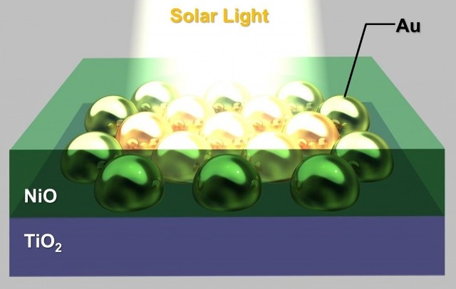
A solid-state solar cell composed of titanium dioxide, nickel oxide, and gold nanoparticles. Gold nanoparticles harvest light and provide a visible light response to the cell. Copyright: Tomoya OSHIKIRI, Hokkaido University
Properties of Plasmon-Induced Photoelectric Conversion on a TiO2/NiO p–n Junction with Au Nanoparticles
Keisuke Nakamura, Tomoya Oshikiri, Kosei Ueno, Yongming Wang, Yoshiomi Kamata, Yuki Kotake, and Hiroaki Misawa
†Research Institute for Electronic Science and ‡Creative Research Institution, Hokkaido University, N21, W10, CRIS Building, Kita-ku, Sapporo 001-0021, Japan
§ Department of Applied Chemistry & Institute of Molecular Science, National Chiao Tung University, 1001 Ta Hsueh R., Hsinchu 30010, Taiwan
J. Phys. Chem. Lett., 2016, 7 (6), pp 1004–1009 DOI: 10.1021/acs.jpclett.6b00291
Abstract
We have successfully fabricated all-solid-state plasmonic photoelectric conversion devices composed of titanium dioxide (TiO2)/nickel oxide (NiO) p–n junctions with gold nanoparticles (Au-NPs) as prototype devices for a plasmonic solar cell. The characteristics of the crystal structures and the photoelectric properties of the all-solid-state devices were demonstrated. We observed that the crystalline structure of the NiO thin film and the interfacial structure of TiO2/Au-NPs/NiO changed significantly during an annealing treatment. Furthermore, the photoelectric conversion devices exhibited plasmon-induced photocurrent generation in the visible-wavelength region. The photocurrent may result from plasmon-induced charge separation. The photoelectric conversion properties via plasmon-induced charge separation were strongly correlated with the morphology of the TiO2/Au-NPs/NiO interface. The long-term stability of the plasmonic photoelectric conversion device was found to be very high because a stable photocurrent was observed even after irradiation for 3 days.
In situ metrology to characterize water vapor delivery during atomic layer deposition
Tariq Ahmido, William A. Kimes, Brent A. Sperling, Joseph T. Hodges and James E. Maslar J. Vac. Sci. Technol. A 34, 031512 (2016) | Read More
Water is often employed as the oxygen source in metal oxide atomic layer deposition(ALD) processes. It has been reported that variations in the amount of water delivered during metal oxide ALD can impact the oxide film properties. Hence, one contribution to optimizing metal oxide ALD processes would be to identify methods to better control water dose. The development of rapid, quantitative techniques for in situwater vapormeasurements during ALD processes would be beneficial to achieve this goal. In this report, the performance of an in situ tunable diode laser absorption spectroscopy (TDLAS) scheme for performing rapid, quantitative water partial pressure measurements in a representative quarter-inch ALD delivery line is described. This implementation of TDLAS, which utilizes a near-infrared distributed-feedback diode laser and wavelength modulation spectroscopy, provides measurements of water partial pressure on a timescale comparable to or shorter than the timescale of the gas dynamics in typical ALD systems. Depending on the degree of signal averaging, this TDLAS system was capable of measuring the water partial pressure with a detection limit in the range of ∼0.80 to ∼0.08 Pa. The utility of this TDLAS scheme was demonstrated by using it to identify characteristics of a representative water delivery system that otherwise would have been difficult to predict. Those characteristics include (1) the magnitude and time dependence of the pressure transient that can occur during water injection, and (2) the dependence of the steady-state water partial pressure on the carrier gas flow rate and the setting of the water ampoule flow restriction.
JVST
A is Soliciting Research Articles for Publication in a Special
January/February 2017 Issue on Atomic Layer Deposition and Atomic Layer
Etching
Submission Deadline: September 6, 2016
These special issues are planned in collaboration with
ALD 2016 Conference and the ALE Workshop being held in Dublin, Ireland, during July 24-27, 2016. The
Special Issues will be dedicated to the science and technology of atomic
layer controlled deposition of thin films. While a significant fraction
of the articles expected are to be based on material presented at ALD
2016 and the ALE Workshop, research articles that are on ALD and ALE but
not presented at this conference are also welcome: the special issue
will be open to all articles on the science and technology of ALD and
ALE.
Thank you to all that have submitted abstracts. Details regarding the format for printing can be found here: Poster Printing Instructions for ALD2016. Please note that all authors are required to print their own posters and the document includes details of a local company that is located close to the Convention Centre.
Conference Registration: Please note if you haven’t already registered place/s for the conference and this must be completed separately here.
Most focus on the reporting for the current Aixtron situation is typically focusing on MOCVD and LED business. However, I find it naturally much more interesesting in the sense of China taking over the ex-Genus ALD business unit based in Sunnyvale (USA). Aixtron is currently on the ALD Top 10 OEM ranking for ALD (Number 7 possibly) and this is a booming market because of multi patterning coming strong now and in the following nodes. Aixtron has a multi wafer ALD plattform that can most probably be used for multi patterning as well so this to me much more interesting potential than their LED business. In addition, Aixtron has had recent success on the Korean DRAM market. So just imagine the new situation if the next grand chip investment will be an etch company.
AIXTRON SE (FSE: AIXA; NASDAQ: AIXG) (“AIXTRON”) and Grand Chip Investment GmbH (“Grand Chip Investment”), a 100% indirect subsidiary of Fujian Grand Chip Investment Fund LP (“FGC”), have today entered into an agreement to take over AIXTRON. Fujian Grand Chip Investment Fund LP is a Chinese investment fund; 51% of which is held by the Chinese business man Zhendong Liu and 49% by Xiamen Bohao Investment Ltd.
Pursuant to the agreement, Grand Chip Investment has today announced its decision to launch a voluntary public takeover offer to acquire all of the outstanding ordinary shares of AIXTRON SE, including all ordinary shares represented by AIXTRON ADS. Under the terms of the agreement, AIXTRON shareholders will be offered 6.00 Euros in cash per each ordinary share. The transaction values AIXTRON’s equity, including net cash, at approximately 670 million Euros and reflects a 50.7% premium to the three-month volume weighted average share price prior to announcement. The offer shall be subject to certain closing conditions, including regulatory approvals and a minimum acceptance threshold of 60% of all of AIXTRON’s outstanding shares.
The agreement sets out the purpose and the principal terms of the transaction with FGC and the future strategy. FGC intends to support AIXTRON’s strategy going forward. R&D competency and AIXTRON’s existing technology shall be maintained at the existing technology centers. FGC has also agreed that AIXTRON shall further strengthen its technology and IP Portfolio, which shall remain vested with AIXTRON, including in Germany. AIXTRON’s existing global set up will be maintained and expanded with AIXTRON’s three technology hubs in Herzogenrath (Germany), Cambridge (UK) and Sunnyvale (USA). Further international technology hubs may be established. AIXTRON’s legal domicile and headquarters shall remain in Herzogenrath, Germany.
In the event the takeover is successful, Martin Goetzeler is to remain CEO of AIXTRON and Dr. Bernd Schulte is to remain in his function as COO. Following a successful closing of the transaction it is anticipated that Grand Chip Investment will nominate four candidates to the six-member Supervisory Board.
The University of Twente’s MESA+ research institute has purchased an advanced Pulsed Laser Deposition (PLD) machine from its research partner, the spin-off company Solmates. This device opens the door to the creation of new materials and chips (or individual chip components), which are constructed as a series of layers, each just one atom thick. The new machine will enable MESA+ to further strengthen its position relative to industry. This is because MESA+ NanoLab’s numerous researchers and external users will, from now on, be able to work on an industrial scale. As a result, new scientific knowledge in the areas of unconventional electronics and advanced materials will be more accessible, as well as more suitable for practical application at an earlier stage.
MESA+, the University of Twente’s nanotechnology research institute, is a leader in the creation of extremely thin layers consisting of just a single layer of atoms. This involves using a laser to transform a material into a plasma, which then condenses on a surface to form an extremely thin layer. By layering multiple very thin layers, one over the other, it is possible to create completely new chips (or individual chip components) and materials with properties that have never been seen before. The technique involved – which was partly developed at the University of Twente – is known as Pulsed Laser Deposition (PLD). Arjen Janssens, CEO of Solmates, expects that by around 2020 PLD will have evolved into one of the standard chip production systems.
Recently (April 21, 2016) The North California Chapter of The American Vacuum Society (NCCAVS) Thin Film User Group organized a meeting on Advanced Memory in San Jose, California. Now all the presentations by Intel, Globalfoundries and Avalanche Technology are now available for download at the TFUG Proceedings page!
The Thin Film Users Group (TFUG) focuses on state-of-art thin-films deposition and applications for semiconductor and related fields, such as nanotechnology, renewable energy, imaging devices, design for manufacturing, and advanced memory research. It is composed of engineers and scientists from device manufactures, semiconductor equipment venders and universities. The TFUG's main activity is a bi-monthly half-day open seminar from researchers and industry technologists with technical presentations on topics of current interests.
This event was chaired by Chakku Gopalan (Intel Corporation), Co-chared by Chari Perera (Applied Materials Deposition Products Group), Paul Werbaneth (Intevac, Inc.) and Michael Oye (UCSC).
NAND Flash: Where are we, where are we going?
Pranav Kalavade, Principle Engineer at Intel, Non-volatile Memory Solutions Group, Santa Clara.
Two of the speakers, Dr. S.I. Lee (CTO Veeco) presenting “Low Temp Spatial ALD for Multiple Patterning Materials ” and Dr. Jean Marc Girard (CTO Air Liquide) presenting “ALD Precursor Development Challenges for HVM” as well as being part of the conference committee. There will be an opportunity to meet both gentlemen ALD 2016 in Dublin.
Hiromichi Enami form Hitachi High-Tech will be attending ALD 2016 and ALE 2016. Here he is asking CMC Co-Chair Ed Korczynski if he plan to come to Dublin.
Part of Team ZyALD(TM): Ravi Laxman (Linde), Jonas Sundqvist, Ashotosh Misra (Air Liquide) and Jean Marc Girard (Air Liquide). All of whom will come to Dublin!
Rasirc presenting “Hydrazine as a Low Temperature Nitride Source: Materials Challenges for High Volume Manufacturing ” at the event, posing Dan Alvarez CTO and Jeff Spiegelman President and Founder. Bothe gentlemen will attend, present and exhibit at ALD2016!
Angel Yanguas-Gil, a staff scientist at Argonne National Laboratory‘s Energy Systems Division, and Jonas Sundqvist happy to meet again at ALD 2016 in Dublin!
Jonas Sundqvist, Co-Chair of ALD2016 is attending the Critical Materials Conference (CMC 2016) on the 5th and 6th May in Hillsboro, Oregon. Check out his ALD2016 polo!
For attendees still in need of access, please email us
Don't forget to Plan for CMC Conference 2017
May 4, 2017, Dallas, TX (tentative)
This year's conference was a success, bringing together attendees from both business and technical backgrounds. "Development is no longer completely separate from the business aspect of production - both
R&D and manufacturing segments must understand the different
technological and market dynamics of critical materials to plan for
profitable semiconductor IC fabrication," commented TECHCET's President, Lita Shon-Roy.
Throughout the conference, the common theme was the importance of manufacturing-oriented material design. Tim Hendry's presentation elaborated on this, touching on every front end material segment category. Norm Armour
connected all these concepts, highlighting the importance of minimizing
carbon footprints through recycling and improved manufacturing
efficiency.
Here's What the Attendees Had to Say:
"Upon our return we concluded that CMC should be on the recurring conference list."
"Very good meeting. Great focus on key issues."
"Excellent content - practical issues and challenges discussed."
"The event was a wonderful event to attend and I learned a lot."
"Very good conference - good speaker lineup, good content, stimulating topics."
Here is a very nice and informative and forward looking interview of Dave Hemker CTO of Lam Research by Ed Sperling who is the editor in chief of Semiconductor Engineering. The interview covers key issues on for semiconductor process and
manufacturing and the recent developments that will govern the semiconductor industry in the future like 3DNAND, Cross-Point Memory Technology and "Atomic-Level Engineering", which is yet another readout of ALE besides the beer classifications. Please do read the full interview at Semiconductor Engineering and below you will find some answers and statements that I found interesting from an atomic level point of view :
One-On-One: Dave Hemker, Semiconductor Engineering, May 19th, 2016 -
By: Ed Sperling
"Predicting the end of Moore’s Law is like predicting a bear market. Eventually you’re going to be right."
The terms "bull market" and "bear market" describe upward and downward market trends, respectively. Here these the statues of the two symbolic beasts of finance, the bear and the bull, in front of the Frankfurt Stock Exchange. [Wikipedia]
David Hemker is senior vice president and chief technology officer at
Lam Research, where he is responsible for long-range research and
technology development.[www.lamresearch.com]
Atomic-Level Engineering
Hemker: "All of the feature sizes now are on the order of nanometers. The
variation is on the order of Angstroms because you have a 10 Angstrom
window. Our critical feature control has to be under 0.5nm. That’s 5
Angstroms. A bond length is 2.5 Angstroms. We’re doing atomic-level
engineering. That’s one of the new tools we’ll need. You need to peel
off one layer in such a way that you have a perfect etch front, the same
way you will need perfect conformality."
Sperling: "Isn’t that the tradeoff, namely how we get enough throughput and still manage to have that kind of control?"
Hemker: "Yes. The good thing is that from an etch and
dep perspective, as things are getting smaller they’re also getting
thinner. There are lots of circumstances now where you can look at how
much ALD
is used in multi-patterning. Because you’re putting less material down,
you don’t have to add half a micron. You can do 10nm in a very
reasonable time frame, so ALD and ALE become very economical."
Leuven (Belgium) – May 17, 2016– At the
Quantum Europe conference, taking place in Amsterdam, Belgian’s
nanoelectronincs research center imec announced today that it is
ramping-up its R&D activities focused on quantum computing. Imec
will implement qubits and supporting nanoelectronic functionality for
quantum computing, leveraging its advanced silicon (Si) platform that
was established within the framework of its industrial affiliation
program with additional support from the EU through e.g. ECSEL projects SENATE and TAKE-5.
Widely
seen as a possible solution to complex computing problems which are
intractable on classical computers, quantum computing uses quantum
physics to create and manipulate quantum states within electronic
devices (qubits) to enhance the performance over that of existing,
‘classical’ approaches. Of the many device proposals for qubit
implementation, the ones compatible with existing Si technology will
provide the most viable solution for interfacing with the outside world.
The Imec Fab with all necessary 300mm equipment to allow advanced sub-10nm CMOS R&D (www.imec.be)
The goal of imec’s initiative is to establish a bridge between
the most advanced transistor technology and emerging quantum technology
options, representing a natural extension of imec’s Si platform. This
will ensure routes to demonstrate the quantum computing functionality
compatible with industries’ platform technologies. Assuming a key
position in the quantum technologies ecosystem, imec will support the
transition of new quantum technologies, from the physics lab to
technology feed into the supply chain. Imec’s platform will help
translate laboratory demonstrators into commercial products. It will be
open for universities, SMEs and industrial partners of imec’s quantum
technologies programs.
“The coming decades will be characterized
by a wave of quantum technology based applications, ranging from
communication, simulation and sensing, to computation. However, to
enable this, the industry will need technical support to adopt and to
integrate these new technologies into products and services”, stated Jo
De Boeck, CTO at imec. “ Imec’s industry relevant Si platform for the
advanced technology nodes, is currently used to screen technology
options for the 5nm nodes and beyond. The same platform is hence the
ideal basis to start implementing quantum devices as quantum effects are
becoming the starting point of developing a quantum platform.”
A bit late but interesting ranking for those of you interested in semiconductor processing equipment. As released in April by VLSI Research. It is also interesting to see that European companies are strong in this market.
There were no changes in the top five rankings list this year due to stable market conditions and the absence of major mergers and acquisitions. Carl Zeiss SMT retained the top spot with sales just above $1B. Edwards, in second place, narrowed the gap slightly with sales of $630M. MKS Instruments once again benefited from the diversity of its product range to hold third position with sales of $540M and Brooks Automation managed to keep fourth place. Advanced Energy had a great year and asserted its dominance of the RF power subsystems market by growing 17% to consolidate fifth place. The big gainer in 2015 was VAT Group, jumping up from eighth to sixth place as it continues to dominate the vacuum valve field. Horiba and Pfeiffer Vacuum ranked seventh and eighth place respectively, with Ichor Systems just managing to stay ahead of Ebara Corporation in tenth place.
VLSIresearch includes vacuum valves as a critical subsystem and as a result VAT Group is included as a Top 10 supplier in this year’s rankings list.
Ultratech-CNT and Professor Thomas Webster at Northeastern University to Research the Use of ALD-Produced Nano-Materials in Medical Applications
SAN JOSE, Calif., May 17, 2016 /PRNewswire/ -- Ultratech, Inc. (Nasdaq: UTEK), a leading supplier of lithography, laser processing and inspection systems used to manufacture semiconductor devices and highbrightness LEDs (HB LEDs), as well as atomic layer deposition (ALD) systems, announced the formation of a research collaboration with Professor Thomas J. Webster, Ph.D. at Northeastern University, to study the use of nano-materials produced via ALD for medical applications. The initial research has focused on inhibiting bacterial growth and inflammation and promoting cell and tissue growth.
Dr. Thomas Webster, Chair and Professor of Chemical Engineering at Northeastern, said, "We are very excited to embark on this collaboration with Ultratech-CNT. While we are in the early stages of this study, the initial results of our work suggest that the materials and processes we are developing could have long-range impact in this field."
Ultratech-CNT Senior Research Scientist Ritwik Bhatia, Ph.D., who has been working closely with Professor Webster, explained, "This type of work is a marked departure from the traditional applications and uses for ALD and dramatically opens up a new field where material science and life sciences intersect. I am extremely pleased to be part of this research program and excited by the potential benefits for healthy surgical outcomes that this research represents."
Arthur W. Zafiropoulo, Ultratech's Chairman and Chief Executive Officer, said, "At Ultratech, we have long maintained and understood that material science would play a key role in moving many emerging technological fields forward. We also feel that it can serve a much larger role, namely in improving the quality of life. In linking the expertise of Prof. Webster and his research group with Ultratech-CNT's ALD group, we believe we are taking steps to solidly and efficiently pursue our scientific and commercial goals."
Imec has developed a low cost Self-aligned quadruple patterning (SAQP) that meet the basic requirements for 7 and 5 nm CMOS FinFET patterning. The technology is based on 193 immersion (193i) lithography and repeated plasma ALD and etching steps as alternative to expensive high resolution EUV lihography. You can read all details SPIE Newsroom (abstract below).
UPDATE: According to information received spacers are Plasma Enhanced ALD SiO2 and the a-Si mandrel and SiN all from ASM. The etching has been performed using Lam Research chambers.
Self-aligned quadruple patterning to meet requirements for fins with high density
Efraín Altamirano-Sánchez, Zheng Tao, Anil Gunay-Demirkol, Gian Lorusso, Toby Hopf, Jean-Luc Everaert, William Clark, Vassilios Constantoudis, Daniel Sobieski, Fung Suong Ou and David Hellin
Transmission electron microscopy (TEM) images of the stages of SAQP
show, from left to right: patterning of the first core onto a mandrel;
deposition of SiO2 by ALD; etching of the first spacers; etching of the mandrel to produce the second core; further deposition of SiO2by ALD; and etching of the second spacers and silicon nitride pad (14 May 2016, SPIE Newsroom. DOI: 10.1117/2.1201604.006378 ).
Repeated plasma deposition and etching steps enable the patterning of fins with the potential to meet requirements of N7 and N5 technologies for profile, depth, uniformity, and pitch walk. Over recent decades, continuous reductions in the scale of field-effect transistors in accordance with Moore's law, which states that the number of transistors in an integrated circuit doubles every two years, have enabled continuous increases in device performance and transistor density. Currently, state-of-the-art devices are based on structural elements with dimensions of 7nm or even 5nm (N7/N5). The highest-resolution patterns required for N7/N5 devices are silicon fins with a pitch of 18–28nm and metal layers with a pitch of 24–32nm. These dimensions far exceed the resolution attainable with 193 immersion (193i) lithography. Extreme UV lithography might be an alternative process for the formation of lines and spaces, but is expensive and not entirely ready for use in production.
Right now there is a brief window of opportunity to feed in to consultations on the future topics for H2020 funding - in particular, the 2018-2020 workplan for NMPB. Some academic and industrial members of HERALD have therefore put together the enclosed position document on urgent research directions, under the overall heading of 'atomic-level processing'.
The document is public. If you feel it is worthwhile, please circulate it to your colleagues, national/regional funding agencies and in particular to your national contact points and delegates on European committees and technology platforms.
It is hoped that this document will evolve into a "Roadmap for Atomic Layer Processing" over the coming months and years. So please feel free to suggest corrections and improvements. Remember that this is a high-level document aimed at non-experts, not a scientific treatise.
As the next step, we are organising an industry panel discussion on this topic on the morning of Wednesday 27th July at the upcoming ALD2016 conference in Ireland.
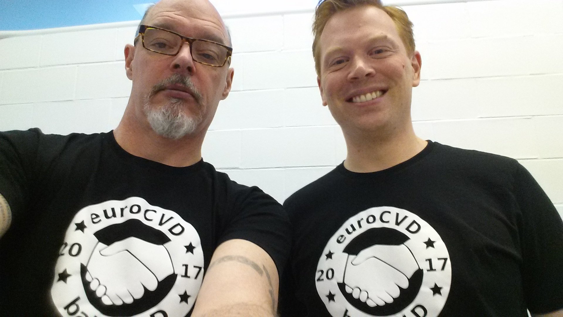
This is an update on the CVD-ALD bonanza that
will take place in Linköping, Sweden 2017. We will organize a joint
EuroCVD-BalticALD meeting over four packed days 11-14 June 2017.
The conference is now open for sponsoring & booking of Trade Show Exhibition space. Please let us know if you have any special wishes for this event and welcome to Sweden in summer of 2017!
Organizing Committee:
Henrik Pedersen, Linköping University, Chair
Jonas Sundqvist, Lund University / Fraunhofer IKTS
Sean Barry, Carleton University
Mats Boman, Uppsala University


%20(1).png)


 These special issues are planned in collaboration with


