Sunday, June 28, 2015

ALD History reading to re-activate, more voluntary contributors welcome

The volunteer-based Virtual Project on the History of ALD (VPHA), launched about two years ago (AVS ALD 2013, San Diego), has already significantly advanced our understanding of the history of ALD. It has become clear that ALD has been invented twice independently of each other, under different names, at different times and geographical locations. 


The main VPHA activity, reading and commenting on early ALD works up to 1986, has so far resulted in three joint publications (see http://vph-ald.com/Publication%20Plan.html). It is getting time to complete the reading and create at least one more publication, aimed at the AVS ALD 2016 conference.

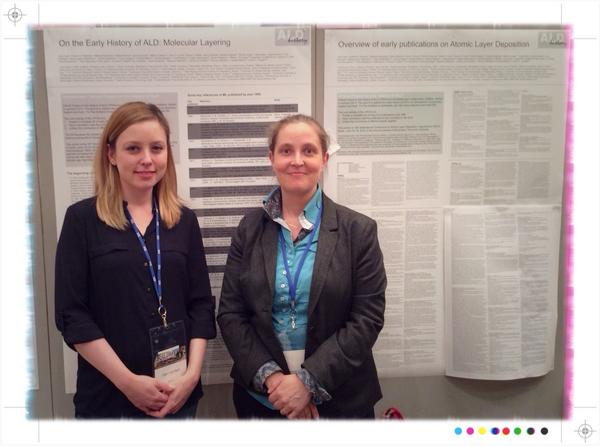
AVSALD 2014 #ALDep conference: the two #VPHA posters, with co-authors from Bilkent (Riikka, Twitter)


VPHA in numbers: 

* There are currently 325 ALD papers listed up to year 1986. 
* About 1000 comments to be given (at least three comments per paper). 
* 36 people from ten countries and >20 affiliations have already given comments in the ALD-history-evolving-file. 
* There is room for many more to join and contribute.


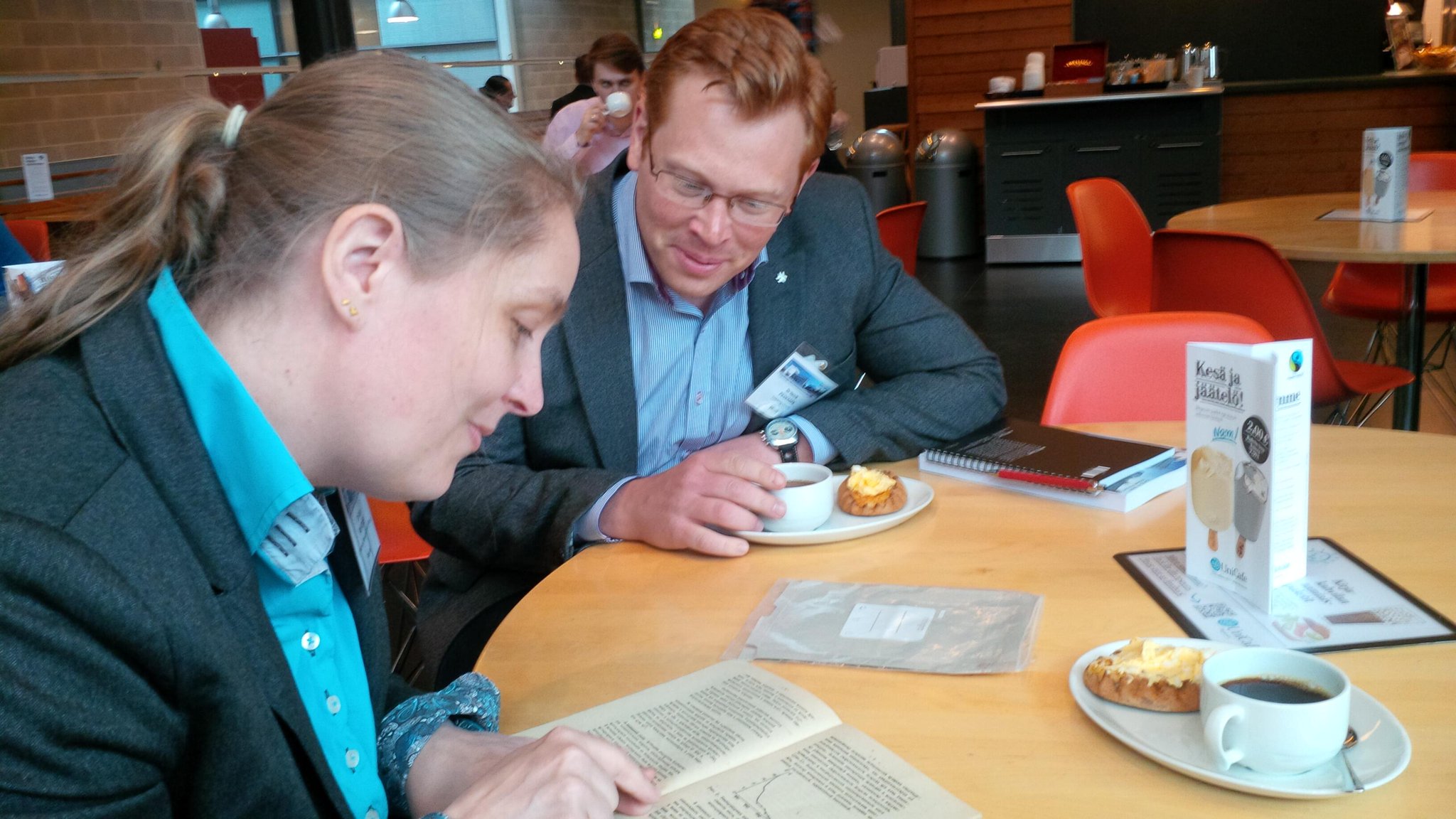
Baltic ALD 2014 in Helsinki: Eating Finnish Pirogs and reading Russian ALD papers looking for the first reference for HfO2 by ALD (Riikka and Henrik)

The condensed publication plan of VPHA is below; full publication details you find from the website created for the VPHA collaboration: http://vph-ald.com. There is also a LinkedIn group, with discussions related to the VPHA and other ALD history aspects:https://www.linkedin.com/groups/ALD-History-5072051/about


...and then the answer pointed out by Prof. Drozd himself.

If you are interested joining this unique international collaborative effort, we warmly welcome you on board. For an active start, you can directly add comments in the ALD-history-evolving-file. We are also in the process of creating a “workflow” which will guide one to read the articles that need it the most.


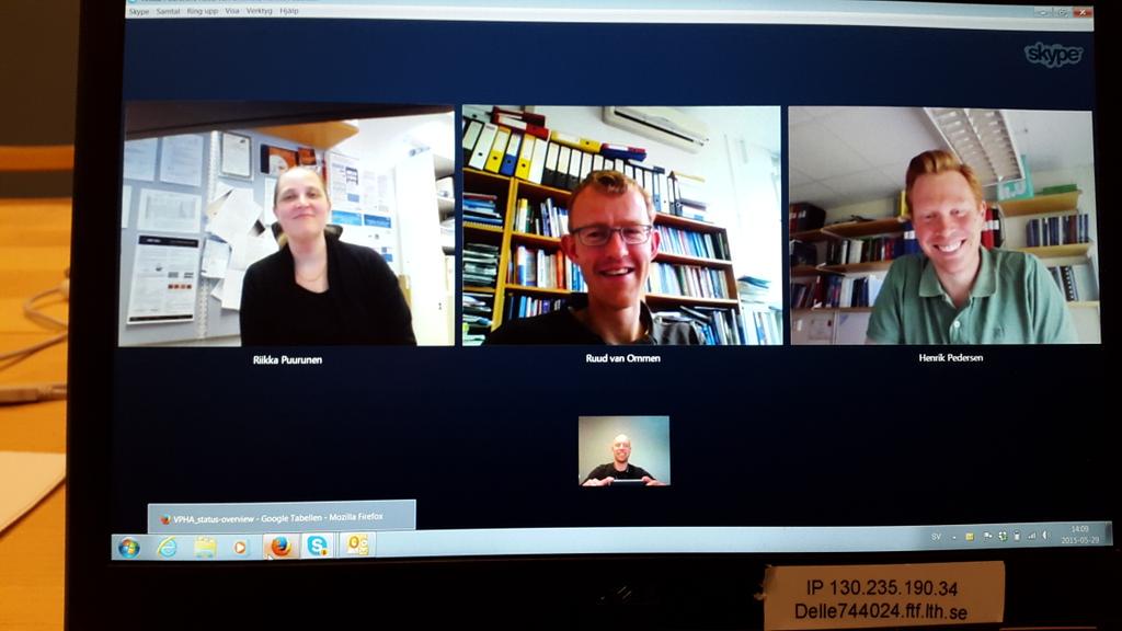
Skype call planning for the VPHA reading project (Riikka, Ruud, Henrik and Jonas)

Info on the progress of “the workflow” and other things will be shared in the ALD History LinkedIn group and through occasional emails to the VPHA authors and prospective authors. To join this VPHA email list, please send me (Riikka) a message - either reply to this post, send a LinkedIn message, or email riikka.puurunen@vtt.fi. 

Best regards, 
Riikka Puurunen, the (unofficial) VPHA coordinator 

--- 

1) Poster at Baltic ALD 2014 - done 
2) Poster at ALD 2014, Kyoto - done 
3) Presentation at ALD 2014, Kyoto - done 
4) ALD history tutorial at ALD 2014, Kyoto – done 
5) Essay on the early history of ALE-ALD – done 
6) Website for ALD history and VPHA – done, http://vph-ald.com
7) Exhibition: 40 years of ALD in Finland - Photos, Stories (FinALD40) – done 
8) Review article/essay on the early history of ML-ALD - ongoing 
9) Presentation at ALD 2016 - ONGOING 
10) Optional: general ALD history review article 
11) Updating wikipedia 
12) Closing the VPHA

Micron’s 32-layer 3D NAND for production this year

The Tool makers of advanced semiconductor processing equipment look form inflection points for new advanced processing technology such as ALD. "The inflection points include the move towards multi-patterning. That’s an enormous driver of growth,” “It’s also the move to finFET from planar. It’s planar to 3D NAND, as well as the move to 3D packaging.” - Doug Bettinger, executive vice president and chief financial officer at Lam Research

Doug must be happy to hear that besides Samsung and Toshiba, Micron will move into pilot production of a 32-layer 3D NAND device in the second half of this year according to Electronics Weekly  The entry device will be a 32-layer device (pictured below) and it is believed that 3D NAND does not become cost-competitive with the most advanced planar NAND until it reaches 48 layers and Micron intends to introduce a 2nd generation 3D NAND which is, presumably, a 48-layer device, end of next year.

Micron 3DNAND 32 layer stack device

Saturday, June 27, 2015

Nanopore patterning using ALD Al2O3 hard masks on SOI substrates

Nice to see some work using ALD hard masks from Arizona State University. For really advanced High-k ultra hard to etch hard masks check out this work by Fraunhofer CNT on zirconia ALD hard masks : High Resolution Patterning by Dual Hard Mask Scheme


Nanopore patterning using Al2O3 hard masks on SOI substrates

Xiaofeng Wang and Goryll 
2015 J. Micromech. Microen Michael g. 25 075020

Abstract

Aluminum oxide Al2O3, deposited using amorphous atomic layer deposition (ALD), is a very promising material to be utilized as a hard mask for nano-patterning. We used an aluminum oxide hard mask on a silicon-on-insulator (SOI) substrate to implement a sub-100 nm nanopore process. The transfer of nanoscale patterns via dry etching of the Al2O3 thin film was investigated by comparing etch profiles, etch rates, and selectivity of Al2O3 over PMMA resist, using different gas chemistries such as Cl2, Ar, Ar/BCl3 mixtures, and BCl3 plasma. A selectivity of 1:4 was observed using an inductively coupled plasma reactive ion etching (ICP-RIE) tool with BCl3 plasma, and the sub-100 nm nanopore patterns were anisotropically transferred to the alumina layer from a 250 nm PMMA layer. The dense and inert Al2O3 hard mask showed exceptional etch selectivity to Si and SiO2, which allowed the subsequent transfer of the nanopore patterns into the 340 nm-thick Si device layer and made it possible to attempt etching the 1 μm-thick buried oxide (BOX) layer. Using chlorine chemistry, nanopores patterned in the Si device layer showed excellent anisotropy while preserving the original pattern dimensions. The process demonstrated is ideally suited for patterning high aspect ratio nanofluidic structures.

Photo show from AVS ALD 2015 in Portland

Here all pictures that appear on Twitter (#AVSALD2015) or that people send me (jonas.sundqvist@baldengineering.com) will be collected!


Impressions


Technical program and abstracts posted by Angel Yanguas-Gil on twitter


Julia Winter from http://www.alchem.ie gets her badge. Here you can also see that ASM has sponsored the key chain.

Seminars


Sunday Tutorials : Prof. Markku Leskelä, University of Helsinki, Finland, “ALD Process Development: Solutions to Industrial Challenges” Introduced by Prof. Winter. (Photo by Iain Buchanan)


Chuck Winter opens AVS ALD 2015. Over 750 attendees (!) and 400+ abstracts (Sean Barry, Twitter)


Here is a picture showing quite clear how broad ALD has become these days (Picture from Martin Knaut).

 
Another shot when the before the first pulse of ALD Experts has been injected (Sean Barry, Twitter)


ALD manufacturing session: packed room (Angel Yanguas-Gil, Twitter


Mato Knez giving a plenary on ALD Beyond Electronics (Sean Barry)


The Golden Boy getting ready for his and Canadas great Golden Day - Session B, 9:15: the first ever robust ALD Au metal process. (Sean Barry, Twitter))


Very good talk by Conley on MIIM diodes (Angel Yanguas-Gil, Twitter)


Poster sessions


Our poster on the evolution of ALD is now up! (Angel Yanguas-Gil, Twitter )


Vincent Vandalon wins the graduate student award for best presentation at #AVSALD2015! We are so proud! http://t.co/LU69IPAr4Q


ALD Trade show


The leading supplier of high quality Atomic Layer Deposition (ALD) technology for industrial manufacturing (Picture by Timo Malinen)


Pall Corporation showing their latest filter technology : Learn about precursor #filtration for contamination control in adv. #ALD processes (Twitter)


Pall Corporation Booth at the ALD trade show (Picture from Rob Nine)

EpiValence Booth http://www.epivalence.com (Picture form LinkedIn, Simon Rushworth)


Dinners and Receptions


Applied Materials, Picosun, Air Products and NSI sponsored party (Sean Barry, Twitter).


Applied Materials, Picosun, Air Products and NSI sponsored party (Martin Knaut, http://www.katharinaknaut.com)


Iain Buchanan from Air Products selling tones of high-k precursor (Martin Knaut, http://www.katharinaknaut.com)


Barking at the Moon (Martin Knaut, http://www.katharinaknaut.com)

Portland Sightseeing


Saturday by Sean Barry (from twitter)


The Golden Team from Ottawa Canada has arrived in Portland : These #BarryLab adventurers drove in a (crappy) van from @ottawacity to #AVSALD2015 in Portland. Check out the bumper


Air Products flying in to Portland passing Mount Hood (Iain Buchanan)


Mount Hood (Martin Knaut, http://www.katharinaknaut.com)


View from the hotel (Tero Pilvi)


Same as above later in the evening at one of the Parties. (Julia Winter, Twitter)


Portland view - Moon and Mountain (Tero Pilvi, Instagram)


The Moon rolling in heading for Mount Hood (Martin Knaut, http://www.katharinaknaut.com)


Old Town Chinatown is the official Chinatown of the Northwest section of Portland. The White Stag sign, a former advertising sign, greets those traveling into Old Town on the Burnside Bridge (Photo by Marcel Junige).


Portland sunset (Photo by Marcel Junige).


Portland airport with Mount Hood in the background (Photo by Marcel Junige).


ASM International Hosts ALD Technology Seminar in Portland at AVS ALD 2015

ASM International N.V. (NASDAQ: ASMI and Euronext Amsterdam: ASM) today announces that it will be hosting a technical seminar in Portland, OR, US, on Tuesday June 30, 2015, the second day of the ALD Conference.


In this 'All about ALD' technology seminar, ASM and a distinguished guest speaker will address challenges and opportunities for ALD processes and equipment to manufacture next generations of micro-electronic devices.

The agenda is as follows:

5.30 pm Reception, drinks and food 
6.15-6.30 pm Dr. ir. Ivo Raaijmakers (ASM) - Welcome and introduction
6.30-7.00 pm Dr. Jeffrey Elam (Argonne National Laboratory) - "Selective ALD in polymers: sequential
infiltration synthesis for lithography and nanofabrication " 
7.00-7.20 pm Dr. Suvi Haukka (ASM) - " Present and future challenges of atomic layer deposition"

Following the presentations, there is room for open discussion and networking until 9.00 pm.

The ASM technology seminar will take place in the Skyline room I-II at the Portland Hilton, 921 SW Sixth Ave., Portland, OR, 97204 US. The room will open at 5:30 pm for invited attendees. Interested parties should contact Rosanne de Vries, +31 88 100 8569, rosanne.de.vries@asm.com.


Friday, June 26, 2015

Beneq introduces a PEALD process to deposit silicon nitride on 3D structures with excellent uniformity


To yield superior thin film properties on planar as well as complex 3D structures, Beneq is now launching a highly competitive low-temperature, plasma-enhanced atomic layer deposition (PEALD) process for depositing silicon nitride (Si3N4).


The use of silicon nitride is extensive in many high-tech sectors, including the semiconductor industry, for micro-electromechanical systems (MEMS) and in medical applications. Silicon nitride thin films are ideal when used as chemical barriers and insulators in integrated circuits, or as diffusion barriers for microchips, or as dielectrics in capacitors.

Currently, CVD-based processes are largely used to grow silicon nitride (Si3N4) thin films. Due to the intrinsic mechanisms and properties of CVD processes, coating complex 3D structures with conformal and uniform thin films has been impossible. By introducing a robust and up-scalable Si3N4 process, Beneq is again paving the way for new opportunities in ALD.

The newly launched Beneq process now offers the opportunity to use Si3N4 in 3D structures in the semiconductor industry, for MEMS applications and much more. It features low processing temperatures, starting at 250 °C, for ease of production. The main specifications of the process are:
  • high uniformity on 3D structures
  • low temperature process – starting from 250 °C
  • Si3N4 thin film chemical composition
  • very low level of contaminants
  • safe to use – non-hazardous precursors
  • simple to upgrade – available for Beneq TFS 200 and TFS 500

“We’re really pleased to launch this unique Si3N4 depositing technology,” says Markus Bosund, Senior Scientist at Beneq. “Again, we can reach beyond the limitations of conventional thin film processes and offer a competitive ALD solution. Our PEALD process allows outstanding film properties for 3D structures at low temperatures. For Beneq, this is the next milestone in our history of bringing the world’s best ALD expertise to the market.” 

The process will be formally presented during ALD 2015, the 15th International Conference on Atomic Layer Deposition and main annual event for the global ALD community in research and industry. ALD 2015 will be held June 28th - July 1st, 2015, Portland, Oregon, USA, where Senior Scientist Markus Bosund will be presenting work that Beneq has completed together with Hewlett-Packard Co. and the University of Jyväskylä. The topic of his presentation is: “Saturation Behavior and Film Properties of Plasma-Enhanced ALD Grown Silicon Nitride”. 

Beneq is a pioneer in ALD equipment and applications development, with installed equipment serving university labs, research institutes and corporate R&D worldwide. Beneq is the developer of Roll-to-Roll ALD.

Research and Markets: 2015 ALD/CVD High K and Metal Precursors for the Semiconductor IC Market

Pretty impressive to know that "The semiconductor CVD/ALD industry utilizes precursors for over 29 different metals and metal oxides provided globally by 23 suppliers." Thanks Rob for sharing this one in the ALD LinkedIn Group!

Research and Markets has announced the addition of the "2015 ALD/CVD High K and Metal Precursors for the Semiconductor IC Market" report to their offering.

The High K / ALD Precursors report provides information on the applications and markets associated with front end and back end of line precursors used to produce high dielectric constant (K) dielectrics and atomic layer deposition dielectrics and metals. Market size, growth, and market share statistics are provided.

Rancho Santa Fe, CA, June 15: Use of front-end Ta and W metal gate and Hf gate dielectric precursors will grow over 2.5x by 2020, according to a new report from this research industry, 2015ALD/CVD High K and Metal Precursors for the Semiconductor IC Market. The overall precursor market sits at $185M today, and is expected to grow 18% over the next five years. The advanced metal gate and gate dielectric segments within that market are expected to grow at 168%, more than compensating for the 25% decline anticipated for the high memory precursor segment.

The 2014 market size for CVD/ALD precursors for interconnect applications was approximately $93M, up 19% over 2013. 2015 is forecast to be up another 15%. By 2016, growth in this segment will be dominated by cobalt barrier precursors, as WF for contact and plug applications begins to decline. The 5-year CAGR for this area is forecast to be 9.4% overall.

The precursor market for capacitor CVD/ALD applications, which includes DRAM and a variety of memory devices, is expected to be flat for the next 5 years, fluctuating in the range of $55M to $70M. The difficulties in forecasting conventional memory demand are compounded by the emergence of a host of new memory device structures, not all of which depend on these materials.

The semiconductor CVD/ALD industry utilizes precursors for over 29 different metals and metal oxides provided globally by 23 suppliers. In addition to market analysis, process flow details, precursor candidates and critical supply chain issues, the report includes regional ranking for major suppliers of vapor deposition precursors.

RASIRC to showcase technology leadership in hydrogen peroxide delivery in Portland

OMG it is heating up before the upcoming Atomic Layering weeks in Portland! RASIRC is well prepared. I know by own experience that they have the absolutely best technology there is for delivering hydrogen peroxide. It is sort of embarrassing after having worked and published papers on using a stander bubbler and realizing that I actually did not deliver basically any H2O2 onto the surface back then. Talk to Jeff Spiegelmann at the conferences he will explain it all for you.


RASIRC will showcase technology leadership in hydrogen peroxide gas for next generation semiconductor materials and processes with a poster session and exhibit (booth #39) at the 15th International Conference on Atomic Layer Deposition June 28-July 1 in Portland, Oregon. The company will present a second poster at the Atomic Layer Etching Workshop held immediately following the ALD Conference. The posters are titled “In-Situ Monitoring of Hydrogen Peroxide Vapor Delivery Systems for ALD” and “Novel Hydrogen Peroxide Delivery Systems for Atomic Layer Cleaning and Etch”.

“The ALD Conference and ALE Workshop are great forums for us to discuss our technology around hydrogen peroxide gas, which we believe will be a critical component in enabling next generation ALD and ALE processes,” said Jeffrey Spiegelman, RASIRC President and Founder. “Test results from in-situ monitoring clearly show that H2O2 gas delivery for ALD can be stable with or without water, and that H2O2 gas can remove carbon from ALD pre-initiation layers to eliminate wet cleaning steps.”

In-Situ Monitoring of H2O2 for ALD


H2O2 gas is more reactive with metal precursors than water and less aggressive than ozone. Process engineers can now deliver high concentration H2O2 gas to process with or without water. RASIRC co-developed an analyzer for in-situ monitoring of H2O2 gas to verify the H2O2 gas concentration flowing to process. Test results using the analyzer clearly show stable H2O2 gas concentration over extended periods of time. Tests were performed on both high concentration H2O2 gas delivery systems and anhydrous H2O2 gas delivery systems.

For high concentration systems using 30% H2O2 liquid source, tests showed stable delivery of up to 5% gas by volume. For anhydrous systems, test results showed stable, consistent delivery of virtually water-free H2O2 gas. Test results will be presented at a poster session on June 30 from 5:30pm-7:30pm.

H2O2 Gas for ALE


H2O2 gas for atomic layer etching enables process engineers to eliminate certain cleaning steps in processing next generation semiconductors. Uniform removal of layers is critical to device performance due to layers now being only several atoms thick, and H2O2 gas is ideally suited to this task. RASIRC will present test results showing that high concentration H2O2 gas can be generated and delivered to process at stable concentrations of up to 5% gas by volume. Preliminary test results with new materials and alternative chemistries will also be shown. The poster presentation will be on July 1 from 6:00pm-9:00pm.

ALD Conference Presence


For more information about H2O2 Gas with or without water, ALD Conference attendees are invited to visit RASIRC in booth #39. Representatives will be available to discuss technologies and test results.


CVD of vertically aligned silicon nanowires in MEMS using silane as a precursor

Here is a very good and detailed paper on CVD of vertically aligned silicon nanowires in MEMS using silane as a precursor by researchers at Catalonia Institute for Energy Research (IREC), Institute of Microelectronics of Barcelona, and ETH Zurich. Pretty high aspect ratio - Open Access - enjoy!

Towards a full integration of vertically aligned silicon nanowires in MEMS using silane as a precursor

G Gadea, A Morata, J D Santos, D Dávila, C Calaza, M Salleras, L Fonseca and A Tarancón
G Gadea et al 2015 Nanotechnology 26 195302


Samples with R = 168 and tdip = 30 s grown during 60 min at 32 mTorr of silane pressure (2.5 Torr total pressure) at different growth temperatures: (a) 520 °C; (b) 630 °C; (c) and (d) 725 °C ((d) shows a 20° tilted view). In (a), (b), and (c) higher-magnification insets show the nanowires at their middle section for diameter comparison. The inset in (d) shows a higher magnification of the nanowire tips from sample (c).

Abstract

Silicon nanowires present outstanding properties for electronics, energy, and environmental monitoring applications. However, their integration into microelectromechanical systems (MEMS) is a major issue so far due to low compatibility with mainstream technology, which complicates patterning and controlled morphology. This work addresses the growth of 〈111〉 aligned silicon nanowire arrays fully integrated into standard MEMS processing by means of the chemical vapor deposition–vapor liquid solid method (CVD–VLS) using silane as a precursor. A reinterpretation of the galvanic displacement method is presented for selectively depositing gold nanoparticles of controlled size and shape. Moreover, a comprehensive analysis of the effects of synthesis temperature and pressure on the growth rate and alignment of nanowires is presented for the most common silicon precursor, i.e., silane. Compared with previously reported protocols, the redefined galvanic displacement together with a silane-based CVD–VLS growth methodology provides a more standard and low-temperature (<650 °C) synthesis scheme and a compatible route to reliably grow Si nanowires in MEMS for advanced applications.

Thursday, June 25, 2015

Saxonian President Tillich propose Euro-Chip Foundry in Dresden


Sachsens Ministerpräsident Stanislaw Tillich. Abb.: J. Jeibmann/Staatskanzlei
The Minister-President of the German Free State of Saxony, Stanislaw Tillich (CDU) propose to the European Commission to build a European Foundry. Obviously he would like to see it built in Dresden.


Today two 300 mm Fabs are operated in Dresden, The Globalfoundries Fab1 running high performance CMOS down to 28 nm and having 22 nm FDSOI in pilot, according to a recent statement made in Grenoble (http://www.eetimes.com/document.asp?doc_id=1326954)

The other 300 mm Fab is the ex-Infineon, ex Qimonda - now Infineon 300 mm DRAM Fab that has been converted to manufacturing power semiconductors on 300mm thin wafers in its CoolMOS family. In addition, XFab has a 200 mm Fab in Dresden

It is not the first time this idea of a European foundry has surfaced in Dresden and it will be interesting to see at SEMICON Europa 6-8 October how serious this bold proposal by Mr. Tillich. We have to remember that it was on his watch when Infineon let Qimonda go down the drain in 2009. One point for discussion will obviously be - if Fab1 is struggling to keep i high utilization today - what products will fill the European Mega Fab. The answer can´t just be IoT and Industrie Vier-Punkt-Null - This would also be a Mega Investment! Let´s be hopeful - Go Tillich!


The Dresden manufacturing site is recognized throughout the industry as among the most successful leading-edge semiconductor production facility in the world. Fab 1 represents one of the biggest international investments in Germany with a total investment to date of more than $7 billion, and about 3,000 world-class engineers, technicians, and specialists. (www.globalfoundries.com)


The Dresden 200 mm site is characterized by a high degree of automation: Fully automated wafer transport, integrated production control and single wafer tracking are central elements. Every week thousands of silicon wafers pass through the highly complex production system in our high end clean room. Infineon Dresden runs production 24-hours a day, seven days a week throughout the year, in a modern and flexible shift system. In July 2011, the Infineon Management Board had decided to establish Dresden as the world's first high-volume production site for power semiconductor devices on 300mm wafers. (www.infineon.com)


The X-FAB Dresden location running analog/mixed-signal CMOS processes (www.xfab.com)

Ultratech-Cambridge NanoTech ships 400th ALD system

Ultratech, Inc., a supplier of lithography, laser­-processing and inspection systems used to manufacture semiconductor devices and high-­brightness LEDs (HB­-LEDs), as well as atomic layer deposition (ALD) systems, announced that its Cambridge NanoTech business unit, Ultratech-CNT, has shipped its 400th ALD system. The system was purchased by the University of Michigan.


Dr. Neil Dasgupta, Assistant Professor of Mechanical Engineering at University of Michigan, whose group received the ALD equipment, said, “Ultratech-CNT’s ALD system has provided a significant boost to our research productivity, enabling us to make rapid advances in the field of surface and interfacial modification of energy conversion devices, including batteries, solar cells, and catalysts. The versatility of the ALD system to address the varied needs of our research program, coupled with the depth of knowledge of their science and engineering team, has enabled us to move very quickly towards producing high-impact research. We are happy to be part of this significant milestone in receiving the 400th system, and we look forward to developing a strong relationship with Ultratech-CNT.”

Ultratech-CNT Vice-President of Research and Engineering, Ganesh Sundaram, Ph.D., said, “It has always been about the scientist and researcher, and about making them successful in achieving their research goals. We are extremely gratified by Professor Dasgupta’s decision to purchase our ALD system. We have known his work since his days as a graduate student at Stanford University, and he has consistently produced noteworthy results using ALD. Looking forward, we are excited by the prospects of the breakthroughs in science that he, along with all other researchers, will be making using our instruments. For our part, we celebrate the shipment of our 400th system and will continue our tradition of providing deep expertise combined with exciting technology.”

Ultratech-CNT’s ALD Systems: 


Savannah G2 ALD System

The Savannah G2 platform incorporates a wide range of advanced field-upgradable options intended to aid serious researchers in expanding their portfolio of available ALD films, as well as allow them to characterize the films in real time.


Phoenix G2 Batch ALD System

Engineered for high throughput, the Phoenix provides maximum uptime in any fabrication environment from pilot production to industrial-grade manufacturing. Technologists and researchers rely on the Phoenix for repeatable, highly-accurate film deposition on flat and 3-D substrates alike for batch production ALD requirements.


Fiji High-Vacuum ALD System

A modular, high-vacuum ALD system, the Fiji series accommodates a wide range of deposition modes using a flexible architecture and multiple configurations of precursors and plasma gases. The result is a next-generation ALD system capable of performing thermal and plasma-enhanced deposition.