


%20(1).png)
Here is a great piece by ED KORCZYNSKI, Senior Technical Editor at Solid State Technology on the practical limits for metallization beyond 14nm tthat inspired me too dig into ALD Mn self forming barriers.
Ed states that one of the limitation for Cu metallization will actually be how thin you can deposit an ALD barrier/seed layer (see figure below).

So guys we need better Metal ALD processes for highly conductive
metallization barrier/seed materials and ultimately replace Cu with
something else - but what? Mn has been heavily investigated as a so
called self forming barrier by Imec, Tyndall, Harvard, Applied Materials
and Intel and presented at different conferences. Another candidate is
Ru but it´s always a candidate for any application, but never makes it
really due to that it is too expensive or some blistering formation or
poor nucleation - all sort of excuses.
Imec has announced (EE Herald, 2013) "it has developed a Manganese (Mn)-based self-formed
barrier (SFB) process that significantly improves Resistance Capacitance
(RC) performance, via resistance and reliability in advanced
interconnects. It provides excellent adhesion, film conformality,
intrinsic barrier property and reduced line resistance."

Here is a slide from a Tyndall project started in 2013 with Applied Materials and iTech explaining the concept of Mn self forming barrier (SFB). Full presentation can be found here.
It seems to be possible to deposit extremely thin and functional self forming Mn barriers by ALD (see figure below). However, until this point in time Mn has not appeared in any reverse engineering as I am aware of and that means that 14nm most probably don´t have Mn One major issue that I heard though with Mn that it is not CMP friendly and possibly this is one reason why it has not come into play yet - who knows though what will appear at 10 nm?
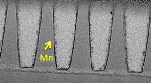
 One way to shrink the nanosized wires (cross sections shown here)
that interconnect electronic circuit components is to replace the
“thick” tantalum nitride-like film used today to encapsulate the copper
core (left) with a thinner manganese silicate film made via ALD. (From a previous blog post)
One way to shrink the nanosized wires (cross sections shown here)
that interconnect electronic circuit components is to replace the
“thick” tantalum nitride-like film used today to encapsulate the copper
core (left) with a thinner manganese silicate film made via ALD. (From a previous blog post)
The ITRS Interconnects Roadmap for barriers and conductors as publishes at the ITRS Summer Meeting (July 2015) has Mn barrier introduction next year which would mean the 10 nm node.
 ITRS Interconnects Roadmap for barriers and conductors (ITRS Summer Meeting July 2015).

The ITRS Interconnects Roadmap for barriers and conductors as publishes at the ITRS Summer Meeting (July 2015) has Mn barrier introduction next year which would mean the 10 nm node.

No comments:
Post a Comment