


%20(1).png)
Check it out - this is like the coolest thing I have ever seen so far - the two leading ALD High-k products (DRAM & High performance CMOS) merged into one ultra high performance graphics chip by AMD. TechInsights has investigated the AMD Fury X cards in their lab and published it in a series of articles in EE Times:
Accordingly, SK Hynix announced its high bandwidth memory (HBM) product in early 2014, claiming it to be the world’s first 8Gb module made using 2Gb, 20nm node, DDR4 SDRAM. Now the HBM modules has shown up in product - AMD’s Radeon 390X Fury X graphics card.
According to TechInsight : "Hynix disclosed a via middle process for their HBM in two papers (Electronics Components & Technology Conference 2013 and VLSI Tech. Digest 2014). The TSV openings are formed after the tungsten contacts to the gates and source/drain regions are made, using a Bosch TSV etch. An oxide liner is then deposited along the via sidewalls, lined with a Ta-based barrier and Cu seed layers, and filled with electroplated Cu. A thermal anneal process is used as a Cu stress relief. A CMP and etch process is used to thin the backsides of the DRAM wafer and expose the Cu TSVs. The backsides of the DRAM wafers are then passivated with oxide, followed by the formation of the backside micro bumps."
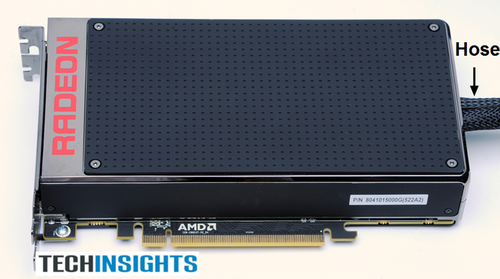
AMD Radeon Fury X (Source: TechInsights)
Some facts from the reports:
- The GPU die has four Hynix HBM memory modules arranged around its perimeter.
- Both the GPU and the HBM modules are flip-chip bumped to a UMC fabbed interposer.
- The interposer is, in turn, bumped to a laminate substrate.
- The GPU itself is a massive measuring in at 23mm by 27mm large, and is believed to be fabricated using TSMC’s 28nm HKMG process.
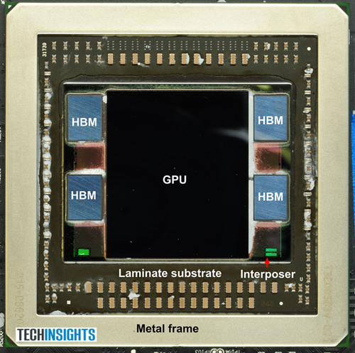
"The GPU die is seen in the center of the module with four Hynix HBM memory modules arranged around its perimeter. Both the GPU and the HBM modules are flip-chip bumped to a UMC fabbed interposer. This interposer is, in turn, bumped to a laminate substrate. The GPU is massive measuring in at 23mm by 27mm large, and is believed to be fabricated using TSMC’s 28nm HKMG process." (EE Times, TechInsight)
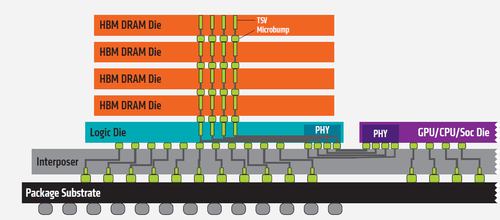
Schematic cross section of HBM module. (Source: AMD HBM brochure, TechInsights)
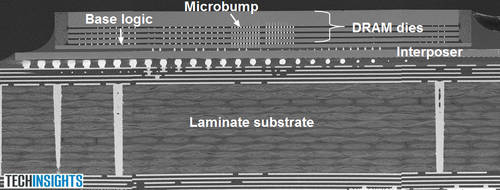
Hynix HBM memory (Source: Package Analysis of the SK-Hynix HBM, TechInsights)
No comments:
Post a Comment