


%20(1).png)
An exciting day today in the middle of Swedish vacation times as we made the first experience with Atomic Layer Etching (ALE) at Lund Nano Lab.
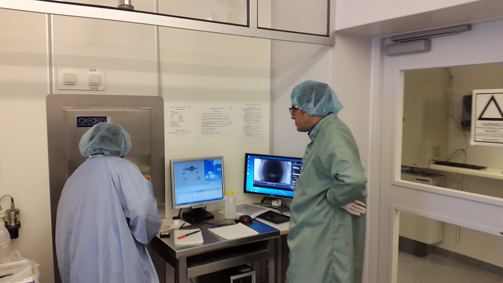
Reza Jafari Jam instructing us and learning all the tricks on etching with the Oxford PlasmalabSystem 100.
We use a Oxford Instrument PlasmalabSystem 100 and the rather well studied Ar-plasma- Purge-Cl2-Purge sequence to etch silicon form the device layer of a 300mm FD-SOI wafer that we diced up in 10x10 mm coupons

Our Master student on ALE Sabbir Khan adjusting the first recipe that Dmitry Suyantin wrote before going on a well deserved vacation

The first plasma cycle - you can almost sense the saturation here ...

Unloading the first sample after 10 ALE cycles - looks pretty much like we have removed some Ångströms per cycle here - how many we will have to see when the elipsometer model for the stack is put to test.

Pristine 10x10 mm SOI coupon samples next to the etched one - elipsometer tells us we removed 2-3 Å but the fit is really bad so we need to get that reconfirmed later.
Stay tuned for more updates and yes we will move to etching III/V nanowires as soon as we can say that we master etching silicon layer by layer.
No comments:
Post a Comment