Thursday, July 31, 2014

Nanofabrication on bumpy or multilevel surfaces using ALD presented by Aalto University

Nanofabrication on bumpy or multilevel surfaces is often a problem; even for the most accurate state-of-the-art methods. Now, reporting in Nanotechnology, researchers at Aalto University in Finland have established a rapid fabrication process that may provide a solution. They utilize atomic layer deposition (ALD) of ion-sensitive resist for the very conformal coating of non-planar sample surfaces. The key feature is the exposure of patterns by focussed ion beam (FIB), which has a large depth of focus in comparison to e-beam or UV lithographies.
 
 
The application of ALD and FIB effectively solves the problems with resist deposition and exposure. The difficulties associated with non-uniform etching speed are addressed by solely utilizing dry etching for both the resist development and release etching steps.


Revolutionary microshutter technology by NASA improved ALD

NASA technologists have hurdled a number of significant technological challenges in their quest to improve an already revolutionary observing technology originally created for the James Webb Space Telescope.


The team, led by Principal Investigator Harvey Moseley, a scientist at NASA’s Goddard Space Flight Center in Greenbelt, Maryland, has demonstrated that electrostatically actuated microshutter arrays — that is, those activated by applying an specific voltage — are as functional as the current technology’s magnetically activated arrays. This advance makes them a highly attractive capability for potential Explorer-class missions designed to perform multi-object observations.
“We have identified real applications — three scientists want to use our microshutter arrays and the commercial sector has expressed interest,” said Mary Li, a Goddard engineer who is working with Moseley and other team members to fully develop this already groundbreaking observing technology. “The electrostatic concept has been fully demonstrated and our focus now is on making these devices highly reliable.”

[...]

Through experimentation, the team used atomic layer deposition, a state-of-the-art fabrication technology, to fully insulate the tiny space between the electrodes to eliminate potential electrical crosstalk that could interfere with the arrays’ operation.

Full story as reported by NASA here.

Wednesday, July 30, 2014

MIT present self-assembly of ALD functionalised carbon nanotubes

A team of researchers at MIT has presented a new way to make microstructured surfaces - A method can produce strong, lightweight materials with specific surface properties. by employing ALD coatings. The team has created a new way of manufacturing microstructured surfaces that have novel three-dimensional textures. These surfaces, made by self-assembly of carbon nanotubes, could exhibit a variety of useful properties — including controllable mechanical stiffness and strength, or the ability to repel water in a certain direction.

“We have demonstrated that mechanical forces can be used to direct nanostructures to form complex three-dimensional microstructures, and that we can independently control … the mechanical properties of the microstructures,” says A. John Hart, the Mitsui Career Development Associate Professor of Mechanical Engineering at MIT and senior author of a paper describing the new technique in the journal Nature Communications.

The technique works by inducing carbon nanotubes to bend as they grow. The mechanism is analogous to the bending of a bimetallic strip, used as the control in old thermostats, as it warms: One material expands faster than another bonded to it. But in this new process, the material bends as it is produced by a chemical reaction.
 
 
Close-up microscope images of carbon nanotube forms and illustrations of the patterns that produce them. At left, a simple curved form, and at right, complex curved propeller shapes, that can be produced by this carbon nanotube growth method. (MIT News)


The process begins by printing two patterns onto a substrate: One is a catalyst of carbon nanotubes; the second material modifies the growth rate of the nanotubes. By offsetting the two patterns, the researchers showed that the nanotubes bend into predictable shapes as they extend.

“We can specify these simple two-dimensional instructions, and cause the nanotubes to form complex shapes in three dimensions,” says Hart. Where nanotubes growing at different rates are adjacent, “they push and pull on each other,” producing more complex forms, Hart explains. “It’s a new principle of using mechanics to control the growth of a nanostructured material,” he says.

Few high-throughput manufacturing processes can achieve such flexibility in creating three-dimensional structures, Hart says. This technique, he adds, is attractive because it can be used to create large expanses of the structures simultaneously; the shape of each structure can be specified by designing the starting pattern. Hart says the technique could also enable control of other properties, such as electrical and thermal conductivity and chemical reactivity, by attaching various coatings to the carbon nanotubes after they grow.

“If you coat the structures after the growth process, you can exquisitely modify their properties,” says Hart. For example, coating the nanotubes with ceramic, using a method called atomic layer deposition, allows the mechanical properties of the structures to be controlled. “When a thick coating is deposited, we have a surface with exceptional stiffness, strength, and toughness relative to [its] density,” Hart explains. “When a thin coating is deposited, the structures are very flexible and resilient.”

This approach may also enable “high-fidelity replication of the intricate structures found on the skins of certain plants and animals,” Hart says, and could make it possible to mass-produce surfaces with specialized characteristics, such as the water-repellent and adhesive ability of some insects. “We’re interested in controlling these fundamental properties using scalable manufacturing techniques,” Hart says.

Hart says the surfaces have the durability of carbon nanotubes, which could allow them to survive in harsh environments, and could be connected to electronics and function as sensors of mechanical or chemical signals.

Kevin Turner, an associate professor of mechanical engineering and applied mechanics at the University of Pennsylvania who was not involved in this research, says this approach “is quite novel because it allows for the engineering of complex 3-D microstructures [composed] of carbon nanotubes. Traditional microfabrication approaches, such as patterning and etching, generally only allow for the fabrication of simple 3-D structures that are essentially extruded 2-D patterns.”

Turner adds, “A particularly exciting aspect of this work is that the structures are composed of carbon nanotubes, which have desirable mechanical, thermal, and electrical properties.”

Along with Hart, the research team included Michael de Volder of Cambridge University; Sei Jin Park, a visiting doctoral student from the University of Michigan; and Sameh Tawfick, a former postdoc at MIT who is now at the University of Illinois at Urbana-Champaign. The work was supported by the European Research Council, the Defense Advanced Research Projects Agency, and the Air Force Office of Scientific Research.
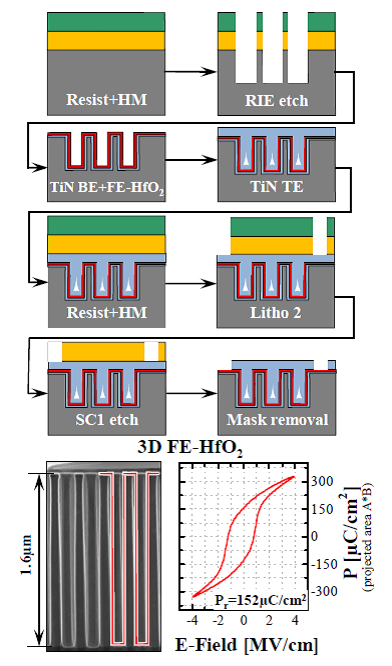
Tuesday, July 29, 2014

VIDEO : An overview on Atomic Layer Etching (ALEt) from Stanford

VIDEO : An overview on Atomic Layer Etching (ALEt)  created for Stanford Nanomanufacturing Class July 2014. Thanks Annina at ALDPulse.com for sharing this!
 
 
Screendump - explaining self aligned double pattering (SAPD) and cration of silicon fins for leading edge FinFETs.


Video on ALEt as published on Youtube.com

Wednesday, July 23, 2014

ECS JSS Special issue on Atomic Layer Etch (ALEt) and Atomic Layer Clean (ALC)

As announced by JSS : Atomic Layer Etch (ALEt) and Atomic Layer Clean (ALC) are emerging as enabling technologies for sub 10nm technology nodes. At these scales performance will be extremely sensitive to process variation. Novel technologies will be required to control variation without increasing complexity if successful introduction of ALEt and ALC into manufacturing schemes is to be achieved. At even more aggressive nodes where novel 2D materials are being considered, the need for zero damage and quasi-infinite selectivity to underlying films or substrates becomes increasingly important.
                          
Atomic layer processes are the most promising path to deliver the precision needed at this scale. However, many areas of ALEt and ALC are in need of improved fundamental understanding and process development. This focus issue will cover state-of-the-art efforts that address a variety of approaches to ALE and ALC. Specific topics of interest include but are not limited to:
  • Surface reaction chemistry and its impact on selectivity
  • Plasma ion energy distribution and control methods
  • Novel plasma sources and potential application to ALEt & ALC
  • Innovative approaches to atomic layer material removal
  • Novel device applications of ALEt & ALC
  • Process chamber design considerations
  • Advanced delivery of chemicals to processing chambers
  • Metrology and control of ALEt & ALC
  • Device performance impact
  • Synthesis of new chemistries for ALEt & ALC application
  • Damage free surface defect removal
  • Process and discharge modeling


Submission Deadline: Dec. 17, 2014

Please submit manuscripts at http://ecsjournals.msubmit.net
Please be sure to specify your submission is for the JSS Focus Issue on
Atomic Layer Etching and Cleaning


Guest Editors:
Dennis Hess
dennis.hess@chbe.gatech.edu
Stefan De Gendt
stefan.degendt@imec.be
Craig Huffman
craig.huffman@sematech.org
Jean-Francois de Marneffe
jean-francois.demarneffe@imec.be
Makoto Sekine
sekine@plasma.engg.nagoya-u.ac.jp

Tuesday, July 22, 2014

Riber signs distribution agreement with CVD & ALD firm AnnealSys

As reported by Semiconductor Today: Riber S.A. of Bezons, France, which manufactures molecular beam epitaxy (MBE) systems as well as evaporation sources and effusion cells, has signed a distribution agreement with AnnealSys SAS of Montpellier, France, which specializes in vapour-phase chemical deposition processes.

The Annealsys MC050 is a 2-inch multi process system (DLI-CVD, DLI-ALD, MOCVD, RTP and RTCVD) offering the widest capabilities for development of new materials (source AnnealSys.com).
 

AnnealSys designs and produces rapid thermal annealing (RTA) furnaces and chemical vapour deposition (CVD) and atomic layer deposition (ALD) systems, which make it possible to deposit complex materials for a wide range of applications, from semiconductors to solar cells, LEDs and microsystems.

AnnealSys’ equipment is aimed primarily at research laboratories and universities, while also meeting the needs of industrial operators for producing small batches. Founded in 2004, the firm has built up unique CVD and ALD expertise, particularly for the integration of direct liquid injection vaporizers, making it possible to implement a wide variety of chemical precursors and to develop processes for growing new materials.

Initially, the partnership between Riber and AnnealSys will focus on CVD and ALD products and the American and Asian regions.

With this commercial agreement, AnnealSys is aiming to accelerate its sales growth internationally by capitalizing on Riber’s sales capabilities and reputation in the research community.

Riber says the agreement represents an opportunity for it to continue moving forward with its technical diversification into other thin-film deposition techniques. The firm says that the commercial partnership will strengthen the range of equipment and services that it offers. The development is also in line with the diversification strategy presented to shareholders at the latest general meeting.
 

Monday, July 21, 2014

'Nano-pixels' promise thin, flexible high-res displays by phase-change films

University of Oxford reports - A new discovery will make it possible to create pixels just a few hundred nanometres across that could pave the way for extremely high-resolution and low-energy thin, flexible displays for applications such as 'smart' glasses, synthetic retinas, and foldable screens.


Still images drawn with the technology: at around 70 micrometres across each image is smaller than the width of a human hair. (Source, University of Oxford)
 
A team led by Oxford University scientists explored the link between the electrical and optical properties of phase change materials (materials that can change from an amorphous to a crystalline state). They found that by sandwiching a seven nanometre thick layer of a phase change material (GST) between two layers of a transparent electrode they could use a tiny current to 'draw' images within the sandwich 'stack'.

Initially still images were created using an atomic force microscope but the team went on to demonstrate that such tiny 'stacks' can be turned into prototype pixel-like devices. These 'nano-pixels' – just 300 by 300 nanometres in size – can be electrically switched 'on and off' at will, creating the coloured dots that would form the building blocks of an extremely high-resolution display technology.
 

Schematic representation of the thin-film material stack comprising ITO/GST/ITO.

Continue reading:  http://www.ox.ac.uk/news/2014-07-10-nano-pixels-promise-thin-flexible-high-res-displays# and a report of the research has been published in this week's Nature.

Also EE Times has more on this story here.

Sunday, July 13, 2014

Ferroelectric deep trench capacitors based on Al:HfO2 for 3D nonvolatile memory applications

P. Polakowski, S. Riedel, W. Weinreich, M. Rudolf, J. Sundqvist, K. Seidel, J. Muller
Memory Workshop (IMW), 2014 IEEE 6th International
Date of Conference: 18-21 May 2014 Page(s): 1 - 4 Print ISBN: 978-1-4799-3594-9 Conference Location : Taipei, Taiwan DOI:10.1109/IMW.2014.6849367
 
Aiming for future nonvolatile memory applications the fabrication and electrical characterization of 3-dimensional trench capacitors based on ferroelectric HfO2 is reported. It will be shown that the ferroelectric properties of Al-doped HfO2 ultrathin films are preserved when integrated into 3-dimensional geometries. The Al:HfO2 thin films were deposited by ALD and electrical data were collected on trench capacitor arrays with a trench count up to 100k. Stable ferroelectric switching behavior was observed for all trench arrays fabricated and only minimal remanent polarization loss with increasing 3-dimensional area gain was observed. In addition these arrays were found to withstand 2∗109 endurance cycles at saturated hysteresis loops. With these report the 3D capability of ferroelectric HfO2 is confirmed and for the first time a feasible solution for the vertical integration of ferroelectric 1T/1C as well as 1T memories is presented.
 

Process flow scheme for the fabricated ferroelectric deep trench capacitors with high aspect ratio of 13:1 and the accordingly measured hysteresis loop of a 3D deep trench capacitor


IBM Zürich solves 40+ Year Old Challenge for Phase Change Materials

IBM Research reports in their News Blog on a breakthrough made in understanding and development of phase change memory cells by IBM Research in Zürich. "... for more than 40 years scientists have never measured the temperature dependence of crystal growth, due to the difficulties associated with the measurements which are taken at both a nanometer length and a nanosecond time scale. That was until earlier this year when, for the first time, IBM scientists in Zurich were able to take the measurements, which is today being reported in the peer-review journal Nature Communications."
 
 
The Binnig and Rohrer Nanotechnology Center is a unique facility for exploratory research. It is not a production or a pilot line with fixed processes or wafer sizes. Rather, it is a state-of-the-art exploratory cleanroom fabrication facility combined with "noise-free" labs shielded against external vibrations, acoustic noise, electromagnetic fields and temperature fluctuations.
 
Please see the abstract to the publication below and check out the blog more details including also an interview with the resreachers at The Binnig and Rohrer Nanotechnology Center in Zürich.
 
  
Abu Sebastian, Manuel Le Gallo und Daniel Krebs (Bild: IBM Research)

Abu Sebastian, Manuel Le Gallo, & Daniel Krebs,
Nature Communications Volume: 5, Article number: 4314 DOI:doi:10.1038/ncomms5314, 07 July 2014

In spite of the prominent role played by phase change materials in information technology, a detailed understanding of the central property of such materials, namely the phase change mechanism, is still lacking mostly because of difficulties associated with experimental measurements. Here, we measure the crystal growth velocity of a phase change material at both the nanometre length and the nanosecond timescale using phase-change memory cells. The material is studied in the technologically relevant melt-quenched phase and directly in the environment in which the phase change material is going to be used in the application. We present a consistent description of the temperature dependence of the crystal growth velocity in the glass and the super-cooled liquid up to the melting temperature.
 
 
The cross-sectional tunneling  electron microscopy (TEM) image of  a mushroom-type PCM cell  is shown in this photo.
 

Saturday, July 12, 2014

Self assembly of 15,000 semiconductor chips per hour

The Next Big Future Blog reports on a A first automated reel-to-reel fluidic self-assembly process for macroelectronic applications. The system enables high speed assembly of semiconductor dies (15,000 chips per hour using a 2.5 cm wide web) over large area substrates. The optimization of the system (hour 99% assembly yield) is based on identification, calculation, and optimization of the relevant forces. As an application the production of a solid state lighting panel is discussed involving a novel approach to apply a conductive layer through lamination.

A First Implementation of an Automated Reel-to-Reel Fluidic Self-Assembly Machine 
Se-Chul Park , Jun Fang , Shantonu Biswas , Mahsa Mozafari , Thomas Stauden , and Heiko O. Jacobs
Adv. Mater. 2014, DOI: 10.1002/adma.201401573 (Free down load)

In this communication, we report on recent progress towards a fi rst implementation of a self-assembly machine that is based on surface-tension-directed-self-assembly. The reported assembly process is no longer a discontinuous smallbatch hand-operated process but resembles an automated machine like process involving a conveyer belt and a reel-to-reel (RTR) type assembly approach with automated agitation. As a comparison, the assembly rate of conventional chip level pick-and-place machines depends on the cost of the system and number of assembly heads that are used. For example, a highend FCM 10000 (Muehlbauer AG) fl ip chip assembly system can assemble approximately 8000 chips per hour achieving a placement accuracy of 30 μm. 

Our current design achieves 15 k chips per hour using a 2.5 cm wide assembly region which is only a factor of 2 better than one of the faster pick-and-place machines; scaling to 150 k chips per hour, however, would be possible using a 25 cm wide web, which would be a factor of 20 faster. 


In principle, scaling to any throughput should be possible considering the parallel nature of self-assembly. In terms of placement accuracy our precision increase with a reduction of chip and solder bump size. Generally, it exceeds the 30 μm limits for the components that have been used. Under optimized operational conditions, we achieved an assembly yield of 99.8% using the self-assembly process. As an application the assembly machine is applied to the realization of area lighting panels incorporating distributed inorganic light emitting diodes (LEDs).


Friday, July 11, 2014

IBM is investing $3 billion to push the limits of chip technology to 7 nm and beyond

Nanowerk News reports: IBM today announced it is investing $3 billion over the next 5 years in two broad research and early stage development programs to push the limits of chip technology needed to meet the emerging demands of cloud computing and Big Data systems. These investments will push IBM's semiconductor innovations from today's breakthroughs into the advanced technology leadership required for the future.


IBM infoographic

Peeling back the layers of thin film structure and chemistry

Nanowerk News reports: Perovskites — any material with the same structure as calcium titanium oxide (CaTiO3) —continue to entice materials scientists with their ferroelectricity, ferromagnetism, catalytic activity, and oxygen-ion conductivity. In recent years, scientists realized that they could vastly improve the properties of perovskites by assembling them into thin films. The problem was that no one understood why thin films beat out bulk materials.Researchers gained new insight into thin-film superiority by probing the structure of perovskites at the X-ray Science Division 33-ID-D,E x-ray beamline at the U.S. Department of Energy's Advanced Photon Source (APS), Argonne National Laboratory. They used a groundbreaking approach to tease apart the thin-film structure and chemistry layer-by-layer

Read more: Peeling back the layers of thin film structure and chemistry http://www.nanowerk.com/nanotechnology-news/newsid=36506.php#ixzz37BBtO4pz 


                                              Graphical abstract: Revealing the atomic structure and strontium distribution in nanometer-thick La0.8Sr0.2CoO3−δ grown on (001)-oriented SrTiO3


Zhenxing Feng, Yizhak Yacoby, Wesley T. Hong, Hua Zhou, Michael D. Biegalski, Hans M. Christen and Yang Shao-Horn

Surface segregation in metal oxides can greatly influence the oxygen transport and surface oxygen exchange kinetics critical to the performance of solid-state devices such as oxygen permeation membranes and solid oxide fuel/electrolytic cell electrodes. Unfortunately detecting elemental distributions at the atomic scale near the surface remains challenging, which hampers the understanding of underpinning mechanisms and control of surface segregation for the design of high-performance materials. Using the coherent Bragg rod analysis (COBRA) method, we report the first direct 3D atomic imaging of a 4 nm-thick “La0.8Sr0.2CoO3–δ”/SrTiO3epitaxial film. Of significance, energy differential COBRA revealed pronounced Sr segregation (La1−xSrxCoO3−δ, x 0.4) in the four unit cells from the top surface while complete Sr depletion was detected in the five unit cells from the “La0.8Sr0.2CoO3−δ”/SrTiO3 interface. The drastic strontium compositional changes in the film were associated with large changes in the atomic positions of apical oxygen sites in the perovskite structure. Such Sr segregation tendencies toward the surface were also found in nominal “La0.6Sr0.4CoO3−δ” thin films, which can greatly enhance the surface oxygen exchange properties of oxides. The results presented here show that COBRA and the differential COBRA methods can be used to investigate a variety of electrochemically active systems providing atomic scale structural and chemical information that can help understand the physical and chemical properties of these systems and serve as a basis for comparison with DFT calculations.


Tuesday, July 8, 2014

VIDEO from Lam Research - Engineering at the Atomic Scale ALD & ALE

Cool video from the Lam Reaearch blog - Building Chips a Few Atoms at a Time


Snap shot from the animated video below (youtube.com)

"Atomic layer deposition (ALD) and atomic layer etch (ALE) use cycles of multi-step processes to deposit or remove a few atomic layers at a time, providing chipmakers with the process control needed for next-generation device manufacturing. To see how these technologies work, check out our latest video"

HAM-LET is releasing its new Ultra Fast (UF) Diaphragm Valve for ALD

HAM-LET is releasing its new Ultra Fast (UF) Diaphragm Valve for Atomic Layer Deposition and fast switching applications, at Semicon West in San Francisco, booth no. 1539, from 8-10 July.

"Our UF's unique flow adjustment mechanism, patent pending no. US 61/910,79, allows for exceptional flow tuning during operation," said Eran Pintel, VP Marketing and Sales at HAM-LET.


"Another advantage of our UF diaphragm valve is its outstanding durability and low maintenance, as it offers over 100 million life cycles. The UF series meets the demand for high-precision diaphragm valves that can perform accurately and repeatedly over an extremely large number of cycles, required by ALD applications," said Pintel.

The optional extended bonnet and cooling fin provide a superb solution when precise and repeatable performance in high-temperature applications is required. The UF series offers superior sealing performance and remarkable durability in hazardous environments, under severe demands of ultra fast actuation at high purity applications.

HAM-LET will showcase a live demonstration of the UF series at Semicon West 2014, booth no. 1539.

About HAM-LET Group

Founded in 1950, HAM-LET Group specializes in the design, development production and marketing of high quality instrumentation valves and fittings in a wide variety of materials for high pressure, high temperature and vacuum applications. An accent on quality combined with ongoing research and development has given the company an international reputation for excellence. As a result, HAM-LET Group today is the fastest growing company in this industry. We are Totally Committed to our customers providing highest quality products and best of breed service. Our products are used around the world in a wide range of industries, including Energy, Oil & Gas, Ground Turbines, Chemical and Petrochemical, CNG/NGV, Semiconductor, Analytical and others.

Visit us at: http://www.ham-let.com

Imec Achieve Record for n-PERT Solar Cell with Spatial ALD from SoLayTec

As reported today : Nano-electronics research center Imec, reported today an n-type PERT crystalline silicon (Si) solar cell fabricated on a large area wafer (15.6cm x 15.6 cm) reaching a top conversion efficiency of 21.5%(calibrated at ISE CalLab), claiming that this is the highest efficiency achieved for this type of solar cell on an industrial large area wafer size.

This result will accelerate the adoption of n-type PERT (Passivated Emitter, Rear Totally diffused) solar cells in the industry as it clearly shows the potential for improved conversion efficiencies for next generation standard two side contacted crystalline silicon solar cells. Additionally imec researchers showed recently that n-type PERT solar cells of imec, having a rear emitter, are not affected by reliability risks originating from a front Ni/Cu plated metallization.

The cell reaching this 21.5% conversion efficiency had an open circuit voltage (Voc) of 677mV, a short circuit current (Jsc) of 39.1 mA/cm2, and 81.3% fill factor, and features a rear blanket p+ emitter obtained by boron diffusion. Reliable front metal contacts on an n+ front-surface-field are formed by means of Ni/Cu/Ag plating (3 bus bars grid) using an industrial plating tool from Meco, while the rear local contacts to the p+ emitter were obtained by laser ablation of the rear passivation stack and subsequent physical-vapor-deposition of aluminum. The rear passivation stack includes a thin (<10 nm) Atomic-Layer-Deposited (ALD) Al2O3 layer, deposited with the spatial ALD technique InPassion Lab from SoLayTec.

The adoption of ALD Al2O3 based-passivation for the p+ emitter resulted in an average improvement in cell efficiency of about 0.3% absolute with respect to passivation by wet oxidation. This illustrates the excellent capabilities of ALD for passivation layers in next generation cell concepts like PERC and n-type PERT.

These results have been achieved in the framework of the imec’s industrial affiliation program on advanced silicon solar cells, dedicated to developing high performance and low cost Si PV-technologies. In this program, imec works closely together with industrial and academic partners along the solar cell value chain. Via participation and contribution to this program, these partners support Imec’s developments and obtain early access to new technology solutions in this way accelerating their own product development.


Lam's New Products Deliver Critical Capability for Building 3D NAND Memory Devices

As reported today by Lam Research Corp. : Lam Research Corp. today unveiled its latest thin film deposition and plasma etch products for 3D NAND fabrication. As memory customers begin ramping production of these new devices, greater process control is needed for cost-effective manufacturing. Lam's new systems address this need for three of the most critical steps in forming 3D NAND memory cells: stack deposition (VECTOR® Q Strata(tm)), vertical channel etching (2300® Flex(tm) F Series), and tungsten wordline deposition (ALTUS® Max ICEFill(tm)).


The 3D NAND memory structures now moving to production involve numerous pairs of stacked films. Process variability on both the horizontal and vertical planes must be minimized for critical steps so that each memory cell in the final device delivers similar performance. Otherwise, variation in one step can be transferred and multiplied in subsequent steps, compounding errors and leading to poor device performance and low product yield. With 40 or more pairs of films in the stack, carefully managing even slight process fluctuations is essential. Lam's new products address these stringent control requirements.

As memory customers begin ramping production of these new devices, greater process control is needed for cost-effective manufacturing. Lam's new systems address this need for three of the most critical steps in forming 3D NAND memory cells: stack deposition (VECTOR® Q Strata™), vertical channel etching (2300® Flex™ F Series), and tungsten wordline deposition (ALTUS® Max ICEFill™).


The new VECTOR Q Strata PECVD (plasma enhanced chemical vapor deposition) system is used for depositing multilayer film stacks. For this critical 3D NAND process step, the system can perform both oxide/nitride (ONON) and oxide/polysilicon (OPOP) film stack deposition. To deposit the ultra-smooth, uniform films required to avoid compounding errors, the system's matched chambers deliver superior defectivity, film stress, and wafer bow performance. In addition, the VECTOR Q Strata also provides industry-leading productivity with the highest throughput per square meter of fab area available today. As the number of layers in these stacks continues to grow, high productivity is increasingly important for cost-effective production.

Once the stack of paired films is deposited, Lam's 2300 Flex F Series dielectric etch product is used to create a vertical channel through the stack. The new system can etch through high aspect ratio structures with minimal distortion or sidewall damage, while also tightly controlling etch profile uniformity across the wafer. This capability is critical since even small deviations can cause channel dimensions to differ from cell to cell, resulting in device performance variation. A proprietary high ion energy source with modulation of energies enables these results.

The latest in Lam's market-leading tungsten deposition product line, the ALTUS Max ICEFill system controls variability by providing void-free fill of the geometrically complex 3D NAND wordlines. Using a proprietary filling technique, the new system creates the tungsten wordlines with an inside-out atomic layer deposition (ALD) process. The ICEFill process completely fills the lateral (horizontal) lines without any voids, while at the same time minimizing deposition in the vertical channel area. As a result, both electrical performance and yield are enhanced.

"By focusing on collaboration at Lam Research, we are innovating faster and more effectively to deliver the enabling capabilities our customers need," said Rick Gottscho, executive vice president of Global Products. "With the support and expertise of our customers and research partners, Lam now offers three products -- VECTOR Q Strata, 2300 Flex F Series, and ALTUS Max ICEFill -- that are playing critical roles in the development and production ramp of 3D NAND memory devices."

Sunday, July 6, 2014

Picosun introduces novel ALD metallization solutions

Picosun Oy, presents a range of novel metallization processes for electronics industry. The trend towards more and more compact and miniaturized electronics has forced the manufacturers to invent new methods for packing, stacking, and connecting the active components. Instead of the more traditional horizontal geometry, so-called three-dimensional integrated circuits (IC) and modules in which the components are stacked vertically on top of each other enable denser and more integrated device architecture. This enables continued scaling of technology nodes, faster and more powerful devices, and saves the valuable physical space inside constrained environments such as smartphones and other personal mobile equipment, thus realizing even more versatile and multifunctional end products. 

Picosun’s now developed metallization processes enable several critical applications of the electronics industry such as diffusion barriers, adhesion and seed layers for interconnects, capacitor electrodes for memories, gate metals for logic devices, and TSV (Through-Silicon-Via) structures for 3D packaging. 
 
 
Applications Director at Picosun Wei-Min Li, Ph.D.

“We are pleased to announce these novel processes, developed in collaboration between Picosun and our customers. During the past 20 years of ALD development I’ve come to known the immense industrial relevancy of these processes. These metallization processes will be a yet new essential asset for Picosun as a leading solution provider for today’s and tomorrow’s IC industries,” states Dr. Wei-Min Li, Applications Director of Picosun and the CEO of Picosun Asia, after his invited speech at the AVS ALD 2014 conference in Kyoto, Japan in June.

Picosun’s highest level ALD thin film technology enables the industrial leap into the future by novel, cutting-edge coating solutions, with four decades of continuous, groundbreaking expertise in the field. Today, PICOSUN™ ALD systems are in daily production use in numerous major industries around the world. Picosun is based in Finland, with subsidiaries in USA, China, and Singapore, and a world-wide sales and support network.

Oxford Instruments Seminar at IOP in Beijing 24-25th September 2014

Starting with half day plenary sessions on 2D materials with guest plenary speaker Dr Aravind Vijayaraghavan from the National Graphene Institute in Manchester, UK, and on Quantum Information Processing with guest plenary speaker Prof David Cory from the Institute for Quantum Computing, University of Waterloo, Canada, Oxford Instruments’ seminar at the IOP in Beijing from 24-25th September promises to discuss cutting edge nanotechnology solutions for multiple applications.

 
Two parallel sessions will focus on thin film processing, & materials characterisation, surface science and cryogenic environments and a wide range of topics will be covered within each technical area. These sessions will include guest international and Chinese speakers from renowned research institutions, speakers from the host institute, and technical experts from Oxford Instruments. This will also present an excellent opportunity for networking between all participants.
Confirmed speakers include the following, but more will be announced soon:
  • Dr. Aravind Vijayaraghavan, National Graphene Institute, Manchester, UK
  • Prof David Cory, Institute for Quantum Computing, University of Waterloo, Canada
  • Prof Guoxing Miao, Institute for Quantum Computing, University of Waterloo, Canada
  • Prof Erwin Kessels, Tue Eindhoven, Netherlands
  • Prof. HE Ke, Tsinghua University, Institute of Physics, CAS, China
  • Dr. WANG Xiaodong, Institute of Semiconductors, CAS, China
  • Prof. ZENG Yi, Institute of Semiconductor, CAS, China
  • Prof Robert Klie, University of Illinois Chicago, USA
  • Prof. Xinran WANG, Nanjing University, China
  • Prof. Zhihai CHENG, National Centre for Nanoscience and Technology, China
  • Prof. Yeliang WANG, Institute of Physics, CAS, China
The thin film processing sessions will review latest etch and deposition technological advances, including: ALD, Magnetron Sputtering, ICP PECVD, Nanoscale Etch, MEMS, MBE and more.
Materials characterisation, Surface Science and Cryogenic Environment sessions will cover multiple topics and technologies including: Ultra high vacuum SPM, Cryo free low temperature solutions, XPS/ESCA, an introduction to atomic force microscopy (AFM) and applications such as nanomechanics, In-situ heating and tensile characterisation using EBSD, Measuring Layer thicknesses and compositions using EDS, Nanomanipulation and fabrication within the SEM / FIB.
The host of last year’s Nanotechnology Tools seminar in India, Prof. Rudra Pratap, Chairperson at the Centre for Nano Science and Engineering, Indian Institute of Science, IISC Bangalore commented, “This seminar has been extremely well organised with competent speakers covering a variety of processes and tools for nanofabrication. It is great to have practitioners of the art give talks and provide tips and solutions based on their experience, something that cannot be found in text books.”
“This workshop is a great opportunity for a wide range of scientists in research and manufacturing to discover practical aspects of many new and established processes, technologies and applications, directly from renowned scientists and a leading manufacturer with over 50 years in the industry”, comments Mark Sefton, Sector Head of Oxford Instruments NanoSolutions, “Delegates appreciate the informal workshop atmosphere of these events, encouraging delegates to participate through open discussion and sharing their questions and experiences.”
This seminar is free of charge but prior booking is essential. To register and for more information, visit www.oxford-instruments.cn/NanoWorldChina

Digital Specialty Chemicals HVM production of UHP PDMAT for ALD-TaN

As reported by Digital Specialty Chemicals in a Solid State Technology Blog - An Improved methods of purification have been used to produce microcrystalline pale yellow PDMAT with purity of >99.99995%
 
 
Improved methods of purification have been used to produce microcrystalline pale yellow PDMAT with purity of >99.99995% (determined by trace metals and other spectroscopic methods) with extremely low chloride (<10ppm), low oxygen and total trace metals. (Picture from Solid State Technology Blog)

HVM production and challenges of UHP PDMAT for ALD-TaN

For sub-22nm device generations, device manufacturers are likely to adopt PDMAT precursor for ALD-TaN barrier films for copper interconnect structures.

BY LEIJUN HAO, RAVI K. LAXMAN and SCOTT A. LANEMAN, Digital Specialty Chemicals, Toronto, Ontario, Canada.

At sub-micron device technology, copper is the interconnect metal of choice because of low resistivity, 1.7μΩ-cm, high current densities and excellent thermal conductivity. These characteristics of copper are increasingly important for supporting sub-22nm lines with high device density and speed. Deposition of copper lines can be achieved by a variety of techniques. A standard method generally involves physical vapor deposition (PVD) and electrochemical deposition (ECD). Because copper diffuses into silicon, silicon dioxide, and other low k dielectric materials, which can “poison” the device, Ta/TaN films are used as copper diffusion barriers. Copper integration schemes at sub-22nm use low-k dielectric PVD Ta/TaN barrier/ PVD copper seed/ ECD-Cu material stack.
 
Continue reading here.

JUSUNG Provides Etcher and TSD-CVD Deposition Equipment to CNSE

JUSUNG Provides Etcher and Single Type TSD-CVD Semiconductor Deposition Equipment to CNSE /SUNYIT

In accordance with Governor Andrew M. Cuomo’s commitment to maintaining New York State’s leadership in nanotechnology, the newly merged SUNY College of Nanoscale Science and Engineering (CNSE) / SUNY Institute of Technology (SUNYIT) today announced a strategic partnership agreement with JUSUNG Engineering Co., Ltd. which includes delivery of state-of-the-art equipment for use in production processes of nanoscale computer chips and the location of technical staff from Korea to the Albany Nanotech campus.
 

The $10M partnership, supported by 25 earchers and engineers in Korea and New York, focuses on improving manufacturing efficiency, which is a primary objective in semiconductor manufacturing. The JUSUNG etcher (Model name: Genaon Plus) represents a first-of-its-kind design that includes a core process tool to etch novel material metal layers. The cutting-edge tool enables significantly improved semiconductor chip efficiency that will set the standard for future production processes. In addition, JUSUNG employees stationed at the Albany Nanotech Complex will collaborate with researchers from the newly merged CNSE/SUNYIT and its global corporate partners to develop innovative etching and encapsulation techniques critical for advanced technology nodes.

“The addition of JUSUNG Engineering to our team of global semiconductor leaders and specifically to our processing equipment center is further testament to the technology powerhouse that Governor Cuomo continues to build in New York State,” said Dr. Michael Liehr, Executive Vice President of Innovation and Technology of the newly merged CNSE/SUNYIT. “JUSUNG is world renowned for its work in the semiconductor industry. Their contribution of technical expertise and cutting-edge tools further strengthens the newly merged CNSE/SUNYIT’s world-class capabilities, and we anticipate an exciting and mutually beneficial partnership.”

“Our collaboration with the newly merged CNSE/SUNYIT will have significant impact on semiconductor players around the world,” said JUSUNG CEO, Hwang Chul-joo. “The JUSUNG tool being delivered to CNSE is the first in the world that can provide a complete solution of etch and deposition of new metal materials for next-generation devices. Combined with the vast collection best in class tools and practices already in use at the Albany NanoTech campus, we will drive innovation in the global semiconductor industry while strengthening the next-generation semiconductor equipment market.”

The etcher and single type TSD-CVD to be supplied together is semiconductor deposition equipment that enables simultaneous space and time split while allowing for applicability to various processes including nitridation, oxidation, doping and metal electrode deposition functions on top of traditional Chemical Vapor Deposition (CVD) and Atomic Layer Deposition (ALD). Advantages include the absence of polymer residue after etching is complete; over 200 hours MTBC (Mean Time Between Cleaning); and absence of surface plasma damage.

The JUSUNG Genaon Plus is scheduled for arrival to the Albany NanoTech campus June 29, 2014.

Source: http://www.sunycnse.com/
 
Jusung has previoously supplied a Genaon Plus to CROCUS for MRAM stack ecting as reported here.