Monday, March 31, 2014

Altatech has recieved an order for a CVD system to University of Washington

As reported today in a press release from Altatech, a subsidiary of Soitec, has received an order from the University of Washington in Seattle for an AltaCVD(TM) chemical vapor deposition (CVD) system whose unique combination of capabilities allows users to develop new process materials with high added value. The Altatech's CVD system will be installed at the university's Washington Nanofabrication Facility (WNF), where it will be used by both internal and external researchers in fabricating a broad range of semiconductor-based devices including leading-edge CMOS transistors, MEMS, ICs built with the latest in through-silicon-via (TSV) technology, advanced LEDs and solar cells.

Key features of an Altatech CVD Chamber :


  • Standalone chamber or cluster tool capability with industry standard vacuum handling platform
  • Up to three chambers on one platform (150-200 mm or 200-300 mm)
  • Low chamber volume for compatibility with ALD
  • Proprietary gas-distribution system design with dual channel showerhead for enhanced process performance and repeatability
  • Pulsed injection and vaporization of up to three liquid or diluted solid precursors, with fast activation valves < 20 ms
  • Non-contact and high-residence time vaporization for efficient and residue-free vapor formation
  • Up to 12 reactive gases (200-300 mm system)
  • Uniform substrate heating (< 1 %) up to 650 °C through the use of a ceramic resistive heater
  • 13.56 MHz RF generator for plasma-enhanced deposition
  • 350-450 kHz RF generator for ion-bombardment control
  • Automated liquid and gas delivery systems
  • Proprietary PLC control software and user interface

 
Dr. Michael Khbeis, acting director of the WNF, claims, "The AltaCVD system provides a unique capability that enables researchers to deposit conformal metal films for TSV applications as well as metal oxides and nitrides for high-k dielectrics and piezoelectric materials. The higher deposition rate enabled by pulsed CVD makes ALD (atomic layer deposition) films a tractable solution for scale-up paths toward high-volume manufacturing for our researchers and industrial clients. This ensures a viable pathway from academia to real economic impact in our region."
 
The University of Washington - Washington Nanofabrication Facility (WNF) is a national user facility that is a part of the National Nanotechnology Infrastructure Network (NNIN). Located on the University of Washington, Seattle campus, WNF is a full-service micro- and nanotechnology user facility and is the largest public access fabrication center in the Pacific Northwest, with 15,000 square feet of laboratories, cleanrooms, and user spaces focused on enabling basic and applied research, advanced research and development, and prototype production.

Check out the video below to learn more about WNF.


Picosun and Bosch Team up in ALD

 As reported in a Picosun press release today: Picosun Oy, the manufacturer of leading quality Atomic Layer Deposition (ALD) equipment, delivers advanced ALD technology to Bosch's Corporate Sector Research and Advance Engineering for development of novel ALD processes for new products and applications.


The now announced collaboration between Picosun and Bosch Corporate Research signifies the crucial role of ALD in today's high tech forefront. With its nearly 300,000 employees and 46.4 billion euros of sales (2013), more than 360 subsidiaries and presence in around 150 countries, the Bosch Group is one of the leading global actors in fields such as automotive technology, industrial products, and building products.


"We are very pleased to provide our unmatched ALD expertise to Bosch. Picosun and Bosch already share a history of collaboration. The current delivery of Picosun's ALD technology to Bosch's Corporate Sector Research and Advance Engineering only solidifies this further. At the moment, ALD is breaking through throughout the modern industrial field. The implementation of our ALD know-how in one of the world's most multidisciplinary and diverse industrial giants, along with our other deliveries to several prominent global production customers, truly tells how central method ALD is becoming in today's manufacturing industries," states Juhana Kostamo, Managing Director of Picosun.

Picosun's leading ALD thin film technology enables the industrial leap into the future by novel, cutting-edge coating solutions, with four decades of continuous, groundbreaking expertise in the field. Today, PICOSUN™ ALD systems are in daily production use in numerous prominent industries around the globe. Picosun is based in Finland, with subsidiaries in USA and Singapore, and a world-wide sales and support network.

Sunday, March 30, 2014

Texas Instrument and University of Texas reports a new route to HfO2 ALD on Graphene

ALD HfO2 dielectric has since the introduction of Intels 45 nm technology become the material of choise for most modern scaled trasistor technologies. As reported yesterday SIMIT in Shanghai reports HfO2 growth directly on graphene by ALD  using a H2O/TEMAHf ALD process. Now Texas Instruments and University of Texas Dallas, Department of Materials Science and Engineering reports an alternative rout how to grow ALD HfO2 on the inert graphene surface. In a recent publication in Applied Surface Science, the researchers use reactive E-beam evaporation to create an HfO2 seed ayer on graphene for ALD HfO2 growth. ALD of HfO2 was performed using a Cambridge Nanotech Inc., Savannah 100 ALD reactor (TDMAHf and H2O). Please find the abstract below:

Picture from Wikipedia
 

Scaling of HfO2 dielectric on CVD graphene

S. McDonnell, A. Azcatl, G. Mordi, C. Floresca, A. Pirkle, L. Colombo, J. Kim, M. Kim, R.M. Wallace

Applied Surface Scienece, Vol. 294, 1 March 2014, Pages 95–99
 
The deposition of ultra-thin metal oxides on graphene is challenging due to the inert nature of the sp2 bonded graphene lattice. The feasibility of e-beam deposition of hafnium and hafnium oxide layers as seeds for further growth by atomic layer deposition on graphene CVD graphene is presented here. It is shown that metallic hafnium deposited in an ultra high vacuum environment readily reacts with graphene, forming a metal-carbide, rendering it unsuitable as a seed layer for the deposition of gate oxide materials. The deposition of HfO2 by reactive e-beam under an O2 partial pressure on the other hand eliminates the reaction with the underlying graphene. The uniformity of the e-beam HfO2 seed layers is found to control the uniformity of the subsequent films deposited by atomic layer deposition. Contrary to previous studies on graphite and exfoliated graphene substrates it is found that the uniformity and thickness scalability of atomic layer deposited thin films is limited on CVD graphene, most likely due to transfer induced residues on the graphene surface.

Friday, March 28, 2014

SIMIT in Shanghai reports HfO2 growth directly on graphene by ALD

According to a fresh publication HfO2 can be grown directly on Graphene using a H2O/TEMAHf ALD process. Nanowerk.com reports from the team led by Xinhong Cheng at the Shanghai Institute of Microsystem and Information Technology (part of the Chinese Academy of Sciences), turned to a compound with a very unusual name: Tetrakis(ethylmethylamino)hafnium, or TEMAH. At 80 degrees Celsius (176 degrees Fahrenheit), TEMAH is a gas from which hafnium oxide (HfO2), a proven high-k dielectric can be derived. Unfortunately, getting the HfO2 to stick to graphene wasn't easy. "Using a traditional ALD techniques, we blew TEMAH into the deposition chamber with the hope that the HfO2 produced would be absorbed by the graphene substrate; but it would not stick," says Li Zheng, lead author on the JVSTA paper. "So, we pre-treated the substrate with water because we knew it would be absorbed onto the graphene and likely act as a nucleation [growth initiation] site. And that's what we found. TEMAH is attracted to the absorbed water, allowing a HfO2 layer to grow directly - and tightly - on the graphene surface."


Read more: Need your dielectric to stick to graphene? Just add water http://www.nanowerk.com/nanotechnology_news/newsid=34990.php#ixzz2xILrE6lH
Here is the abstract and link to the paper in JVSTA:

HfO2 dielectric film growth directly on graphene by H2O-based atomic layer deposition


J. Vac. Sci. Technol. A 32, 01A103 (2014); http://dx.doi.org/10.1116/1.4828361

"Due to its exceptionally high carrier mobility, International Technology Roadmap for Semiconductors considers graphene to be among the candidate materials for postsilicon electronics. In order to realize graphene-based devices, thin and uniform-coverage high-κ dielectrics without any pinholes on top of graphene is required. There are no dangling bonds on defect-free graphene surface; it is difficult to grow uniform-coverage high-κ dielectrics on graphene directly by atom layer deposition. Meanwhile, degradation of defects in graphene/high-κ structure is necessary for the optimization of high-κ dielectrics fabrication technology. Here the authors report on a H2O-based atom layer deposition method used for HfO2 growth, where physically adsorbed H2O molecules on graphene surface act as oxidant, and self-limit react with metal precursors to form HfO2 film onto graphene directly. Raman spectra reveal H2O-based atom layer deposition method will not introduce defects into graphene. The surface root mean square of HfO2 films is down to 0.9 nm and the capacitance of HfO2 films on graphene is up to 2.7 μF/cm2, which indicate high quality and compactness of HfO2 films. "

Wednesday, March 26, 2014

ALD saving the sunshine for night: solar fuels from artificial photosynthesis

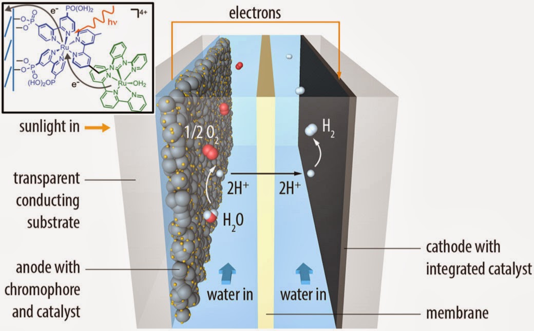
As reported by Thomas Meyer and Ralph House "Saving the sunshine for night: solar fuels from artificial photosynthesis", direct visible light water splitting in a dye-sensitized photoelectrosynthesis cell makes hydrogen for energy storage. Key findings using a stable catalyst is reported by binding on the surface of conducting nano ITO electrodes, they first bind the catalyst to the surface and then stabilize it by ALD of a TiO2 overlayer to prevent hydrolysis.

Dye-sensitized photoelectrosynthesis cell (DSPEC) for water splitting. The inset illustrates the surface-bound chromophore-catalyst assembly (shown as orange dots on the spherical nanoparticles in the core/shell film). H2O: Water. O2: Oxygen. H2: Hydrogen. H+: Hydrogen cation. (Graphic by Yan Liang, L2Molecule.com, as reported in the SPIE news blog)


Read all about it here or check out the original work in these refrences:

T. J. Meyer, J. M. Papanikolas, C. M. Heyer, Solar fuels and next generation photovoltaics: the UNC-CH Energy Frontier Research Center, Cat. Lett. 141(1), p. 1-7, 2011. doi:10.1007/s10562-010-0495-9
 
R. House, L. Alibabaei, C. Bonino, P. Hoertz, J. Trainham, T. J. Meyer, Let the molecules do the work, PV Magazine 03/2013, p. 87-89, 2013.
 
A. K. Vannucci, L. Alibabaei, M. D. Losego, J. J. Concepcion, B. Kalanyan, G. N. Parsons, T. J. Meyer, Crossing the divide between homogeneous and heterogeneous catalysis in water oxidation, Proc. Nat'l Acad. Sci. USA 110(52), p. 20918, 2013. doi:10.1073/Pnas.1319832110
 
L. Alibabaei, M. K. Brennaman, M. R. Norris, B. Kalanyan, W. J. Song, M. D. Losego, J. J. Concepcion, R. A. Binstead, G. N. Parsons, T. J. Meyer, Solar water splitting in a molecular photoelectrochemical cell, Proc. Nat'l Acad. Sci. USA 110(50), p. 20008, 2013. doi:10.1073/Pnas.1319628110

Cambridge Nanotech introducing the Gen 2 of ALD Tools - Savannah & Fiji

As reported today by ALDpulse.com and information on the Ultratech web, Ultratech - Cambridge Nanotech introducing the Gen 2 of ALD Tools - Savannah & Fiji. Check out the fresh looking white design and the Video below for more technical detals.


"Savannah has become the preferred system for university researchers worldwide engaged in ALD and looking for an affordable yet robust platform. We have delivered hundreds of these systems in the past decade."

White pannels instead of polished stailess steal as before. What will Picosun come up with now? Kulta? :-)

New designed gas box
 
 
"Our Fiji series is a modular, high-vacuum advanced thin films ALD system that accommodates a wide range of deposition modes using a flexible architecture and multiple configurations of chambers, precursors and plasma gases.
 
The result is a next-generation ALD system capable of performing thermal and plasma-enhanced deposition."
 
 
New more ergonomic loading of wafers


Tuesday, March 25, 2014

ALD defined by using only the ten hundred most used words

A funny Tweet came along today from Angel Yanguas-Gil : #ald defined using the up-goer five editor: http://t.co/e6L2hItJ. The challenge is Can you explain a hard idea using only the ten hundred most used words?

i grow stuff layer by layer using tiny things that fly through the air and that break down when they touch the stuff I am growing. As they break they form a layer until they don't break anymore. But then I use a kind of air that changes my stuff and lets me start all over again and add a second layer. By repeating this many times, I can get to grow thicker stuff. I grow my stuff inside a sort of can that keeps me from breathing the things i use because they could kill me or make me sick. The stuff that I grow can be used to make computers or get power from the sun.
 
Please do chek out the web page of Angel Yanguas-Gil - it contains amongst other things an equation for ALD:


Monday, March 24, 2014

Good news for ALD "Triple patterning seems like it maybe too expensive to be worth it."

28nm is the last process node that does not require double patterning. At 20nm and below, at least some layers require double patterning, according to Paul McLellan at SemiWiki. Furthermore, he says that SADP/SIT is needed for 10nm for a few layers and then double patterning will be used above that. "Triple patterning seems like it maybe too expensive to be worth it." The same goes for EUV "either there is a miracle in improvement of the power of the light source (and some other problems are solved). Or 10nm slips out several years."

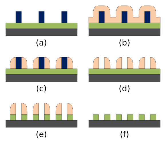
So why is this good news for ALD fanatics? SADP means a good opportunity for conformal ALD processes!  Many cool options are out there, such as ow temperature PEALD or catalytic ALD processes for example. Most commonly SiO2 or Si3N4 is used but assuming selctivity is given you could also use other materials. Check out the last picture below for the process flow for SAPD

Paul McLellan explains the terminology for the future patterning options:
  • double patterning is called LELE (as in Litho-etch-litho-etch or DPT)
  • triple patterning called LELELE (as in Litho-etch-litho-etch-litho-etch or TPT)
  • self-aligned double patterning (SADP) also sometimes called sidewall image transfer (SIT)
  • EUV, 14nm wavelength instead of 193nm, so we can go back to single exposure

 
"Examples of metal routing configuration in design and with double (DPT) and triple patterning technology (TPT), showing the potentially large benefit for pattern density of triple patterning for 1D features. The different colors of the polygon in the decomposed layouts represent the different mask target layouts (two masks for DPT, three masks for TPT)." [Source SPIE/Synopsys Inc.]
 
 
Process flow for multiple patterning process: self-aligned (spacer) double pattering a) features after the photolithographic patterning, b) conformal Si3N4 deposition, c) Spacer production by anisotropic etching, d) removing the resist mask, e) anisotropic etching of the underlying layer (eg poly-Si), f) Final hard mask for the removal of the spacer material with denser lines [Source Wikipedia]


Saturday, March 22, 2014

Meglow hollow cathode plasma source for PEALD reactors reducing oxygen contamination

According to a recent press release: "Meaglow Ltd. (Privately Held) announces a breakthrough in semiconductor production. As computer chips become smaller and smaller, advanced production techniques, such as Atomic Layer Deposition (ALD) have become more important for depositing thin layers of material. Unfortunately the ALD of some materials has been prone to contamination from the plasma sources used. Meaglow Ltd has developed a hollow cathode plasma source which has reduced oxygen contamination by orders of magnitude, allowing the reproducible deposition of semiconductor materials with improved quality."
 
 
"The breakthrough has been shown in a recent publication of oxygen reduction figures for the hollow cathode plasma source supplied last year to the group of Professor Necmi Biyikli, of the Institute of Materials Science and Nanotechnology, at Bilkent University in Turkey. The plasma source was used to upgrade their existing Atomic Layer Deposition (ALD) system by replacing an inductively coupled plasma source. The publication in the Journal of Materials Chemistry C (J. Mater. Chem. C 2 (2014) 2123) shows a reduction in oxygen content of orders of magnitude compared to previous results. There is also a marked improvement in material quality. These results render the older inductively coupled plasma sources obsolete for many applications."
 
Information from the web pageof MEAglow: The hollow cathode plasma source has been designed to allow for a quick  on/off process without major power oscillation. The plasma source also  does not have the oxygen contamination problems that plague many  inductively coupled and microwave plasma sources - due to interaction  between the plasma species and ceramic introduction windows.  Capacitively coupled plasma sources are another plasma source that do  not generally have oxygen contamination problems, however these sources  only have electron densities of 109 to 1010 cm3, in the lower less active region of our hollow cathode source we have measured an electron density of 9x1011 cm3, and a higher density is expected closer to the RF electrode. Another  advantage of this type of plasma source is that it can be scaled by  simply increasing the number of hollow cathode holes.
 
[Source Meaglow.com]
 
 
System Application: Meaglow system, Molecular Beam Epitaxy (MBE), Low Pressure Metalorganic Chemical Vapour Deposition (LPMOCVD), Atomic Layer Deposition (ALD).
 
 
Example of an installation at the Bilkent University ALD System converted for use with a Meaglow Hollow Cathode Plasma Source. Looks like a Cambridge Nanotech Fiji system (?) [Source Meaglow.com]
 
Here is a PDF loaded with Infomration: http://www.meaglow.com/Hollow_cathode.pdf

Samsung: A modified double patterning using ALD allows for continued scaling of DRAM for 10nm class technology

Samsung reports that they are  now mass producing industry’s most advanced 4Gb DDR3, using 20 nanometer process technology:

"Samsung has pushed the envelope of DRAM scaling, while utilizing currently available immersion ArF lithography, in its roll-out of the industry’s most advanced 20-nanometer (nm) 4-gigabit (Gb) DDR3 DRAM."


"With DRAM memory, where each cell consists of a capacitor and a transistor linked to one another, scaling is more difficult than with NAND Flash memory in which a cell only needs a transistor. To continue scaling for more advanced DRAM, Samsung refined its design and manufacturing technologies and came up with a modified double patterning and atomic layer deposition."

"Samsung’s modified double patterning technology marks a new milestone, by enabling 20nm DDR3 production using current photolithography equipment and establishing the core technology for the next generation of 10nm-class DRAM production. Samsung also successfully created ultrathin dielectric layers of cell capacitors with an unprecedented uniformity, which has resulted in higher cell performance."

Here is a folow up blog post from the Samsung Blog: So…About Samsung Mass Producing the Most Advanced 20nm DDR3 DRAM explaining why the dielectric layers (high-k) in the DRAM capacitor memory cell need to be a ‘ultrathin dielectric layer’ for the 20nm DDR3 DRAM compared to the 25 nm cell.

"Why are the 20nm DDR3 DRAM’s dielectric layers ultrathin rather than ultra-thick? Because the thicker the dielectric layers are, the fewer electrical charges are stored in the cell’s transistors; there is simply less room for them. Then how is it that Samsung 20nm DDR3 DRAM’s ultrathin layers are effective?

The material used in the 20nm DDR3 DRAM is measured in Angstrom (Å), a unit of length equal to 10−10 m, basically the size of an atom. The ultrathin dielectric layers of Samsung are composed of atomic materials, aka atomic layer deposition. This is why the amount of electric charges stored in the capacitor of the 20nm DDR DRAM doesn’t change much, in a significantly scale downed cell. Overall, the quality of the each cell of Samsung’s 20nm DDR DRAM is superior to the preceding 25nm DDR3 DRAM. Consequently, 20nm DDR3 DRAM’s superior cells enable high-speed operation, which is the most important characteristic of a DRAM, and low power consumption. Making the dielectric layers of the 20nm capacitor much denser and thinner than the 25nm capacitor was one of the keys to the successful development and now mass producing Samsung’s new 20nm 4G DDR3."

From a Chipworks report abstract that can be bought here, we can see a cross section of the stack capacitor array Samsung is using at 26 nm (see below). For 20 nm I have not been able to find any free available information yet.


The Samsung K4B4G0846C-BCK0 is a 4Gb DDR3 SDRAM manufactured at 26 nm, based on the half minimum pitch ("20nm generation"). The technology features capacitor-over-bitline DRAM cell arrays.

 
Wikipedia on Multiple Patterning: Multiple patterning is a class of technologies for manufacturing integrated circuits (ICs), developed for photplithography to enhance the feature density. The simplest case of multiple patterning is double patterning, where a conventional lithography process is enhanced to produce double the expected number of features. The resolution of a photoresist pattern begins to blur at around 45 nm half-pitch. For the semi conductor industry, therefore, double patterning was introduced for the 32 nm half-pitch node and below, mainly using state-of-the-art 193 nm immersion lithography tools.
 
 
A basic example of a double patterning techniques using Spacer mask: first pattern; deposition by e.g. SiO2 ALD or PEALD; spacer formation by etching; first pattern removal; etching with spacer mask;  final pattern [Source Wikipedia]
 

There are many types of double patterning and when used in combination it iscalled  multiple patterning. Those are:
  • Dual-tone photoresist
  • Dual-Tone Development
  • Self-aligned spacer
  • Double/Multiple exposure
  • Double Expose, Double Etch (mesas)
  • Double Expose, Double Etch (trenches)
  • Directed self-assembly (DSA)
Please see Wikipedia on more information on each type.


Jusung signed a Space Divided Plasma (SDP) system equipment supply contract with SK Hynix


According to a press release from www.businesskorea.co.kr "Jusung Engineering announced on March 20 that it signed a Space Divided Plasma (SDP) system equipment supply contract with SK Hynix. The purpose of this new technology is to respond to next-generation semiconductor device manufacturing processes. The contract makes the first case in which the system is applied to mass production lines."
 
"The SDP system constitutes a part of the atomic layer deposition (ALD) process, which is a key of semiconductor production, and has novel features such as nitridation, oxidation, doping, and film treatment as well as insulating film deposition, conductive film deposition and high k film deposition. Jusung’s equipment is characterized by being capable of overcoming the damage that plasma and high temperatures can do to semiconductor devices while forming the best film quality even at a low temperature. This can contribute to the development and manufacturing of advanced semiconductor devices and easier repair and maintenance of the equipment itself. The SDP system supplied to SK Hynix at this time is a metal film deposition apparatus in particular. It is low resistance and can reduce the electrode resistance value by at least 50 percent compared to existing ones."


The Jusung Cyclone chambers has a 5 wafer rotating heater stage and can operate in Spatial ALD as well as pulsed CVD mode enhancing the troughput considerably for many 3D and thicker film ALD applications. Some examples are High-k, silicon oxide for double patterning and metal electrodes such as TiN. That is why this technology has had success in DRAM industry (Qimonda [R.I.P.], Winbond, SK Hynix, ...) More information from Jusung web on the Jusung Cyclone+ plattform can be found here.

Friday, March 7, 2014

The Xi`an Jiatong University in China purchased a PEALD system from SENTECH in Germany


As reported in a press release: SENTECH Instruments has developed the advanced PTSA (planar triple spiral antenna) inductively coupled plasma source which provides the core plasma technology used in the ICP plasma etcher for low damage and high rate etching and which is used in the ICPECVD low temperature deposition systems. Only recently SENTECH Instruments expanded its ICPECVD processing by ALD and plasma enhanced ALD systems to be able to deposit highly conformal and dense thin metal oxide and metal layers.

The Xi`an Jiatong University in China purchased one of SENTECH`s innovative Atomic Layer Deposition (ALD) systems. The ALD system is equipped with a SENTECH in situ laser ellipsometer and represents a unique tool to monitor and develop new ALD processes. The SENTECH in situ laser ellipsometer used in advanced real time growth process monitoring offers excellent results especially as both tools are made by SENTECH Instruments.

The in situ ellipsometer integrated into the ALD system in Xi'an enables its users to measure film thickness and refraction index of deposited layers during processing with high time resolution. The ALD system was configured for thermal processing and plasma enhanced processing which can be incorporated in recipes without manual interference. Both processes were demonstrated by depositing aluminium oxide (Al2O3).

The contact person at Xi`an Jiatong University is Mrs Ji Xing, technical assistant at the Centre of Nanomaterial for Renewable Energy. She will supervise all experiments and research activities related to the ALD system in the future. After installation and in depth technical training and introduction to processing by SENTECH technical service Mrs Xing was able to operate the ALD and the ellipsometer perfectly by herself.

Quoting Mrs. Xing:

"We are more than satisfied with the smooth professional work of the SENTECH technical service and SENTECH has met all of our expectations concerning the ALD system and its ellipsometer.

The excellent performance of all processes motivated Xi'an University to order additional processes for their new ALD system and SENTECH is glad to provide application support and we are looking forward to further cooperation!"

SoLayTec's Ultra Fast Spatial ALD and motion of wafers by the double floating principle

As reported earlier, Levitech has sipped Spatial ALD equipment to an Asian customer. Levitech is in strong competition with another Dutch Spatial ALD equipment manufacturer, SoLayTec based in Eindhoven. SoLayTec offers a modular concept, either the InPassion LAB tool for optimizing the cell design or an InPassion ALD tool for customers that are already integrating ALD into their production. One advantage is that both products are based on identical core process modules. This makes it easy to ramp-up from low to high volume production.


The user is flexible in choosing a certain recipe, thus adjusting process parameters like layer thickness, precursor flow and deposition temperature  The InPassion ALD consists of 4, 6 or 8 deposition units and has a throughput up to 4500 wph. For maximizing uptime, the tool continues production during a failure of one deposition unit.

 
(a) In spatial ALD the TMA and H2O steps are separated in space by an inert gas (in this case N2). (b) In the deposition unit the wafer oscillates underneath the spatial ALD injector head. (c) The InPassion ALD features two main conveyors  that feeds various ALD units at either side of the conveyor.
 
See more at: http://www.solaytec.com or check out the promotion video below available on Youtube.


Sunday, March 2, 2014

Video from NASA Goddard´s Detector Technology Lab and use of ALD to manufacture QWIPs

 
A video report from Detector Development Lab at NASA Goddard showing the use of ALD amongst other techniques to manufacture QWIPs - Quantum Well Infrared Photodectors. The QWIP detector on Landsat 8 is just one example of many missions supported by the DDL. They have built and packaged detectors to cover wavelengths from X-ray to microwave, in support of missions such as ASTRO-H, SWIFT, HAWC, Suzaku, and JWST.


Video transcript by NASA: As part of NASA's Earth Observing Fleet Landsat has been monitoring the planet's health for over 40 years. With stunning images in multiple wavelengths, Landsat provides valuable data to farmers, scientist, city planners, as well as the public. And behind these images lies QWIP, the Quantum Well Infrared Photodector, which is processed here in the Detector Development Lab at NASA Goddard. Similar to the sensor in your digital camera or cell phone, the QWIP detector is designed to be more sensitive and to detect specific wavelengths. Let me show you how these high-end detectors are created. The spectrum of light contains many wavelengths of which the colors of visible light are a small portion. We have built and packaged detectors to cover wavelengths from Microwave to X-ray The basic goal of a detector is to absorb the energy from a region of these wavelengths of light and turn it into an electrical signal. The first step for us is to take the wavelength, resolution, and sensitivity requirements of the mission and turn that into a detector design using CAD software. The layout is sliced into individual layers or masks that will be combined during fabrication to create the final detector device.
 
Welcome to the Detector Development Lab. This is a unique, Class 100 clean room where we have the agility and technology to develop first-of-a-kind detectors as well as the experience and the process control to turn those into flight qualified products. All of the specialized equipment in this lab is used for 1 of 3 general purposes - Lithography, Etching, and Deposition. Together these 3 processes make up our basic toolset. The first basic process is called Lithography. Don't adjust your picture, the yellow lights provide protection for photoresist, a photosensitive polymer that is used to define the detector geometries to as small as 1 micron. The first step in lithography is to apply photoresist to the substrate. This is done by spinning on a liquid suspension of the polymer in the spin-coater. The coated wafer is taken to the photo-mask aligner, where the chrome-on-quartz mask that was created by the design and layout is placed in extremely close proximity to the substrate and aligned to existing patterns with in a micron of accuracy. A UV light source exposes the photoresist through the mask, transferring the pattern into the photoresist. Finally the substrate is developed, rinsing away the exposed areas of the photoresist.
 
The next step is to use this protective mask and etch to remove material from the exposed areas of the substrate. We have a wide variety of methods for removing materials including wet chemical etchants, reactive plasmas, and ion sputtering. In one of the most fascination examples, the Deep-Reactive-Ion Etcher uses short etching and passivation cycles in a high-power ICP chamber to etch silicon 100's of microns deep with 100:1 aspect ratios. After etching, the photoresist mask is stripped off in a solvent and the substrate is ready for deposition of the next layer of material.
 
 
A Goddard cleanroom process engineer placing a gallium arsenide wafer into the loadlock of a BENEQ TFS 200 ALD process reactor. [screendump 04:05 min from video below]  

Deposition is the third basic process in our toolset and it covers a wide range of specific processes and materials. During deposition, a thin film of material is added back to the surface of the detector's substrate. Materials run the gamut from insulating dielectrics to metal-nitrides, to pure metals and even superconductors. Here in the Atomic-Layer-Deposition system, single atomic layers of materials can be built up one-by-one for precise control of thickness and uniformity. Once the deposition is complete the substrate goes back to lithography to pattern the new layer of material. In building up the designed detector we start with a substrate such as silicon or gallium arsenide wafers.
 
Next, numerous iteration of these 3 basic process steps are applied to the substrate in order to build up the materials and geometry needed to detect the energy of interest such as IR, define the pixels and allow electrical read-out, while meeting all the scientific requirements for the mission. Here is a gallium arsenide wafer with 16 QWIP arrays that has completed fabrication.
 
The substrate is taken to our packaging lab where it is diced into individual dies. The die are screened, then meticulously cleaned and indium-bump bonded directly to a specialized Read-Out Integrated Circuit, which converts the raw electrons generated in each detector pixel to a signal that can be interfaced to the instrument's computers. Finally, the detector and ROIC are bonded to the necessary fixtures and PC boards and the detector subsystem is ready for integration with the rest of the scientific instrument.
 
The QWIP detector on Landsat 8 is just one example of many missions supported by the DDL. We have built and packaged detectors to cover wavelengths from X-ray to microwave, in support of missions such as ASTRO-H, SWIFT, HAWC, Suzaku, and JWST. Each detector was specifically designed to meet the science and mission requirements, developed, fabricated, packaged, tested, and delivered for integration. These unique capabilities at Goddard have helped NASA to stay on the cutting edge of instrument development and scientific discovery. SFX


Another NASA Lab using ALD is NASA/JPL's Microdevices Lab (MDL). According to their equipment list they are operating two ALD systems:  
 
  • Oxford Plasmalab 80 OpAL Atomic Layer Deposition (ALD) System with Radical Enhanced Upgrade
  • Beneq TFS-200 Atomic Layer Deposition (ALD) System
  • Levitech BV sells a Levitrack® ALD system to one of Taiwan’s largest solar cell makers and receives repeat order for second ALD system


    According to a press realse today Levitech BV "announced that one of Taiwan’s largest solar cell manufacturers transferred a Levitrack Atomic Layer Deposition (ALD) system to manufacturing, and placed an order for a second Levitrack system to be shipped in the second quarter."


    “The Levitrack has a proven record in high volume manufacturing and our customer was satisfied with the excellent performance. They decided to order a second system for their expansion for the production of high-efficiency crystalline solar cells. This system will be used for PERC cells - with efficiencies exceeding 20% - , as well as multi-crystalline and n-type products”, said Jaap Beijersbergen, CEO of Levitech.

    “This client chose our Levitrack ALD system based on its significant productivity, cost-of-ownership and process advantages over competitive PECVD and ALD systems for aluminum oxide (Al2O3) applications, Beijersbergen concluded.

    The Levitrack’s unique spatial ALD process and high throughput result in a superior cost-of-ownership of the overall passivation process flow and helps any client to address current and future technology needs.


    Here are some insights from the Levitech web and a YouTube movie (below) into how their Spatial ALD Technology works:

     
    1) The Levitrack™ ALD system is based on the new concept of precursor separation in space, as opposed to time, in combination with the unique floating wafer and conductive heating technology used in the Levitor RTP products. Substrates are floating in a linear gas track, and are heated to the required process temperature (below 300°C) within a matter of seconds. [screendump from youtube movie below]

    2) At process temperature, the substrates float through a series of ALD deposition cells. Each cell consists of 2 precursors, which are separated in space by a Nitrogen purge (acting as inert gas curtains).A sequence of precursor 1, Nitrogen purge, precursor 2, and again, Nitrogen purge will result in the deposition of 1 monolayer. The number of active ALD deposition cells depends on the required layer thickness. [screendump from youtube movie below]


    Saturday, March 1, 2014

    French ALD Equipment supplier Encapsulix has shipped a deposition system to a leading OLED lighting supplier in Europe

    The french ALD Equipment supplier Encapsulix based in Aix-en-Provence has announced that a Gen-2.5 deposition system has been shipped to a "leading OLED lighting supplier in Europe".Encapsulix announced tin October 2013 hat they received such an order and this should then be the shippment - congratulations!
     
    "Encapsulix announced today the sale of an Infinity(tm) 500 manufacturing equipment to a leading OLED lighting manufacturer for Atomic Layer Deposition Encapsulation.
     
    The Infinitytm 500 has been developed utilizing Encapsulix’s patented & proprietary Atomic Layer Deposition technology. The Infinitytm 500 product family deposits barrier and encapsulation films on substrates up to 500mm x 400mm and is the work horse for Gen2 OLED applications. The order received from a leading OLED lighting manufacturer is scheduled to be delivered end of 2013. The system provides the best ultrabarrier performance and cost of ownership for the manufacturing of OLED devices. The Infinitytm 1000 for Gen5 and 5.5 will be introduced in 2014 along with the Infinity tm Flex500 and 1000 for flexible organic substrates and rolls."
     
    According to the information on the webpage the inovation in Encapsulix ALD technology lays in an assembly of modular precursor dosers and gas injectors that behave as a monolithic “unit”
     
     
    Picture from a patent : Gas injection device with uniform gas velocity US 20130019978 A1
    • Assemble application-specific systems based on common technology bricks
    • Factor of 5-100 throughput increase through massive parallel deployment
    • Commonality in hardware, Process between R&D, Prototype, Manufacturing

    Atomic Layer Deposition engineers met in San Diego during SEMATECH’s Q1 Manufacturing Week 17-20th Feb

    As reported earlier here on the ALD News Blog, Atomic Layer Deposition engineers met in San Diego during SEMATECH’s Q1 Manufacturing Week to benchmark ASM, TEL, HKE, AMAT and JUSUNG equipment productivity and to share some best known methods from the HVM Fabs. Samsung, tsmc, Intel, GLOBALFOUNDRIES, IBM, UMC, Winbond, HP and Freescale engineers all participated. The topics of key interest are:

    1) Cost of precursor and dry-precursor usage – taring the weight of dry precursors is not fail safe and therefore not HVM friendly

    2) Cost savings were identified of $800K per tool per year

    3) Some OEM equipment still not being HVM friendly even after 10 years of ALD in manufacturing (HVM hardening & readiness is low compared to other equipment types)

    4) FDC approaches and data collection frequencies (looking at 10Hz for metal ALD right now but potentially requiring 100Hz moving forward)

    5) Trap installation, Helium de-gassers and special fore-line consideration


    Boyd Finlay project manager from Manufacturing Technology at SEMATECH in Albany together with ALD Equipment Engineers and Experts from the top Leading Edge Fabs. 

     
    Atomic Layer Deposition engineers from Samsung, tsmc, Intel, GLOBALFOUNDRIES, IBM, UMC, Winbond, HP and Freescale engineers all participated in the meeting.

    GlobalFoundries and Fraunhofer IIS to collaborate on EUROPRACTICE, Europe’s MPW wafer shuttle program

    Press release
    GLOBALFOUNDRIES and Fraunhofer Institute for Integrated Circuits IIS today announced the extension of their long-term collaboration, focusing on 40nm and 28nm processes. GLOBALFOUNDRIES will also join the European Multi Product Wafer (MPW) Program EUROPRACTICE.


    Through the collaboration GLOBALFOUNDRIES will offer its leading-edge foundry capabilities to Fraunhofer IIS as an aggregator, and Fraunhofer will enable the academic network in Europe to get access to GLOBALFOUNDRIES’ process technologies and Process Design Kits (PDK) via EUROPRACTICE.

    “As one of the largest foundries worldwide and the largest wafer manufacturer in Europe we are proud to enter this prestigious program,” said Karl Lange, GLOBALFOUNDRIES Vice President of Sales for Europe. “With Fraunhofer as channel partner, combined with our broad technology portfolio and process know-how, we will add significant value to EUROPRACTICE.”
     

    “The offer of GLOBALFOUNDRIES technologies down to 28nm to Europe’s universities and research institutes is an important step for EUROPRACTICE and will stimulate education and research in IC design,” said Josef Sauerer, Head of the Integrated Circuits and Systems Department at Fraunhofer IIS. “Also, our contract research with industries will benefit from GLOBALFOUNDRIES’ advanced technology portfolio”

    Fraunhofer IIS and GLOBALFOUNDRIES started their collaboration in 2004 with the successful launch of 180nm and later 55nm programs. The extended collaboration will introduce technology nodes down to 28nm in the European Wafer Shuttle Program, helping European academia and research institutes to get access and support for CAD tools and ASIC prototyping at reduced costs.