Thursday, February 27, 2014

A 3D Printer That Can Build A House way faster than a Fab can Build a CMOS Processor

Researchers Are Making A 3D Printer That Can Build A House In 24 Hours

At The University of Southern California, Professor Behrokh Khoshnevis has built a colossal 3D printer that can build a house in 24 hours.


Khoshnevis’s robot comes equipped with a nozzle that spews out concrete and can build a home based on a set computer pattern. Read the story here.
 

World´s oldest High-k analyzed by Atom Probe!

The World´s oldest mineral analyzed by Atom Probe - a Zircon based High-k! No wonder the DRAM guys finally converged at a ZrO2 based high-k and are stuck in that material since then on. Detailed anylysis by atom probe revield clusters of Yttrium and Lead. Check out the paper by Valley et al of the University of Wisconsin-Madison from the University of Wisconsin-Madison below.
 
 
The nearly 4.4 billion year old zircon, showing examples of clusters of mapped atoms (Picture from ars technica).
 
 
John W. Valley, Aaron J. Cavosie, Takayuki Ushikubo, David A. Reinhard, Daniel F. Lawrence, David J. Larson, Peter H. Clifton, Thomas F. Kelly, Simon A. Wilde, Desmond E. Moser, Michael J. Spicuzza

Nature Geoscience 2014 DOI:doi:10.1038/ngeo2075 Published online 23 February 2014
 
Abstract:
 
The only physical evidence from the earliest phases of Earth’s evolution comes from zircons, ancient mineral grains that can be dated using the U–Th–Pb geochronometer. Oxygen isotope ratios from such zircons have been used to infer when the hydrosphere and conditions habitable to life were established. Chemical homogenization of Earth’s crust and the existence of a magma ocean have not been dated directly, but must have occurred earlier. However, the accuracy of the U–Pb zircon ages can plausibly be biased by poorly understood processes of intracrystalline Pb mobility. Here we use atom-probe tomography to identify and map individual atoms in the oldest concordant grain from Earth, a 4.4-Gyr-old Hadean zircon with a high-temperature overgrowth that formed about 1 Gyr after the mineral’s core. Isolated nanoclusters, measuring about 10 nm and spaced 10–50 nm apart, are enriched in incompatible elements including radiogenic Pb with unusually high 207Pb/206Pb ratios. We demonstrate that the length scales of these clusters make U–Pb age biasing impossible, and that they formed during the later reheating event. Our tomography data thereby confirm that any mixing event of the silicate Earth must have occurred before 4.4 Gyr ago, consistent with magma ocean formation by an early moon-forming impact about 4.5 Gyr ago.

Wednesday, February 26, 2014

Air Products Executive Calls for Collaboration to Maintain Pace of Innovation in Semiconductor Industry

Materials Suppliers and OEMs Need to Work Together to Develop Next Generation Materials

Press Release: True collaboration between material suppliers, OEMs and semiconductor manufacturers is necessary to develop solutions needed to maintain the pace of innovation in the global semiconductor industry. That was the message from Ed Shober, vice president Advanced Materials and Delivery Systems for Air Products (NYSE: APD) who recently spoke at SEMICON Korea's Executive Forum.


For years, materials have played a critical role in the scaling of IC devices. Looking ahead, as device geometries continue to shrink, materials will play an increasingly more critical role in semiconductor manufacturer's success. The move to 3-D structures such as FinFETS and Vertical NAND have created additional material processing steps that require chemical mechanical planarization (CMP), etching and atomic layer deposition to coat and fill structures.
 
"This increasing need for new materials is taxing all of us along the development supply chain," said Shober. "New materials are needed, they must be integrated and the result must not impact cost per wafer, not increase capital cost, not impact yield but must enable high throughput."
 
Materials suppliers have generally assumed the lion's share of the development costs of new materials. These include discovery, applications testing, scaling to manufacture, packaging and analytical, safe and reliable shipping and support at the customer's site. All without the promise of a market and with the risk of materials being quickly commoditized.
 
"We as material suppliers, because of the importance materials are playing in scaling, have reached a critical fork in the road," said Shober. "We can continue down the road we know which will most likely not result in a suitable return on investment or we can choose the road that many have spoken about yet not many have chosen—strategic partnerships. True collaboration can address the problems at hand and develop solutions which enable everyone to share in the success."
 
Device scaling has enabled affordability and far-reaching technologies that has improved countless lives. To continue to make these improvements possible, the pace of innovation must be maintained.
"This requires genuine and close collaboration with a shared vision, so all members of the team know what is required, when it is needed and the economics for the same," noted Shober.

Encapsulation solutions from Dresden presented at ICCG 10

Encapsulation solutions from Dresden presented at ICCG 10
 
As reported in a press release: "The industrial product development focuses more and more on flexible electronics. Thus the technology of organic electroluminescence is on the verge of being launched onto the market. Therefore, high-quality functional films are required in reasonable quantities for the industrial manufacturing of flexible electronic devices. Flexible solar cells based on inorganic or organic semiconductors and flexible organic light-emitting diodes (OLED) provide new possibilities for the integration of photovoltaic or intelligent lighting in buildings and commodity items. Even flexible displays or innovative packaging concepts for pharmaceutical and cosmetic products are on their way to commercialization. All mentioned products have one thing in common: The active layers have to be protected from humidity and oxygen in order to guarantee a reliable functionality over the product lifetime.
 
Currently, the encapsulation technologies for these flexible electronic devices are mostly still in the research or pilot stage. The cluster FLEET – a Fraunhofer initiative - combines the competences of three Fraunhofer Institutions (FEP, IWS and COMEDD), one institute of the Technical University Dresden (IAPP) and one medium-sized company (SEMPA Systems) in this area of expertise. The intention of the cluster is the fast further development of encapsulation technologies to make them ready for the industrial and serial production, by an intensive cooperation along the value chain concentrated at one location."
 
Cluster FLEET will presents its expertise at ICCG 10 (The International Conference on Coatings on Glass and Plastics - Advanced Coatings for Large-Area or High-Volume Products) from 22nd until 26th June 2014, in Dresden.
 
 
You can save more than 25% with the early bird fee and register until March 3, 2014 for the event.
 
Furthermore there are a lot of sponsoring opportunities. Book your exhibition space here for presenting your services and products to  an excellent community of experts. Fraunhofer COMEDD will also offer a company tour on Friday, June 27, 2014. You can register for it also at the organizer of the conference.
 
For all information regarding sponsorship, preliminary program as well as the registration form, please take a look at the homepage: http://www.iccg10.de/


Industrial Robotics Boost Picosun's Production ALD Systems

Press Release: Picosun Oy, the leading Atomic Layer Deposition (ALD) equipment manufacturer, has expanded its selection of high volume manufacturing solutions by launching a patented, fully automatic sample handling system based on industrial robotics.

The customer proven robot loading system is ideal for Picosun's large scale batch ALD reactors such as the PICOSUN™ P-300B and PICOSUN™ P-1000 models. An especially efficient production rate can be achieved by clustering several P-300B batch ALD tools together and synchronizing the sample loading and unloading of the individual tools with the robot.
 
Sample handling with an industrial robot is particularly suitable when processing large amounts of 3D objects such as automotive components and other mechanical engineering products, coins, OLED displays, powders, and articles for decorative coatings. Typically these are items which, when packed in large batches, require a sturdy and fast loading system capable of smooth handling of heavy loads, especially considering the high production throughput requirements for many industries. Batch pre-heating and/or post-deposition high temperature may also render manual handling impossible.
 
Naturally, also large batches of silicon wafers or glass sheets can be easily manipulated with a robot.
In addition to industrial robotic systems, the sample handling options available for PICOSUN™ ALD tools now include a linear loader, vacuum load lock, central vacuum robot sample handling unit (for vacuum cluster configurations), pneumatic chamber lift (for manual operation), and loading through an inert atmosphere glove box.
 

"We are pleased to expand our already unrivalled selection of sample loading options with industrial robotics. The possibility to integrate fully automatic robot operation with our large scale production ALD tools enables us to technologically breakthrough to completely new high volume manufacturing application areas previously unknown to ALD," states Mr. Timo Malinen, Chief Operating Officer of Picosun.
 
Picosun's leading ALD thin film technology enables an industrial leap into the future by novel, cutting-edge coating solutions, with four decades of innovative and pioneering expertise in the field. Today, PICOSUN™ ALD systems are in daily production use in numerous prominent industries around the globe. Picosun is based in Finland, with subsidiaries in USA and Singapore, and a world-wide sales and support network.


Tuesday, February 25, 2014

Journal of Vacuum Science & Technology A Special Issue on Atomic Layer Deposition for AVS ALD 2014

AVS-ALD 2014 in Kyoto har reported that Journal of Vacuum Science & Technology A is soliciting research articles for publication in a Special January/February 2015 Issue on Atomic Layer Deposition.


This special issue is planned in collaboration with the 14th International Conference on Atomic Layer Deposition (ALD 2014) to be held in Kyoto, Japan during June 15-18, 2014. The Special Issue will be dedicated to the science and technology of atomic layer controlled deposition of thin films. While a significant fraction of the articles are expected to be based on material presented at ALD 2014, research articles that are on ALD but were not presented at this conference are also welcome: the special issue will be open to all articles on the science and technology of ALD.

Check te conference program for more information here.
 
Invited Speakers (Confirmed)

Prof. Jiyoung Kim, Univ. Texas at Dallas, USA, “Ozone Based ALD”
Dr. Scott Clendenning, Intel, USA, “New chemical routes into ALD materials and their applications”
Dr. Toshihide Nabatame, NIMS, Japan, “Characterization of several Higher-k films fabricated by Th- and PE-ALD process”
Prof. Yongfeng Mei, Fudan Univ., China, “Atomic layer deposition as a new tool for interdisciplinary research”

Monday, February 24, 2014

Webinar Taking Nano to the next level. Speakers from LBNL and Seagate!

Webinar "Taking Nano to the next level" on 26th March 2014 Presented by keynote industry speakers. Hosted by the IOP on Wed 26th March at 5pm (GMT), 9am Pacific Time.
 

This webinar is free of charge, and will run for 1 hour including time for questions and answers at the end. A focus on recent nanoscale etch and atomic layer deposition (ALD) advances from research to
manufacturing applications, from industry leading speakers: 

Talk 1: ALD and nanoscale etch processing techniques and results from recent work carried out at Lawrence Berkeley National Laboratory (LBNL), USA

Speaker: Deirdre Olynick, Staff Scientist, LBNL, CA, USA

Talk 2: Data storage, an expanding market application that has benefited from advanced ALD and nanoscale etch techniques

Speaker: Kim Lee, Seagate, CA, USA

Worldwide Smart Coatings Markets forecast 2013-2020

A new report on how "Smart Coatings" will evolve the years to come. No mentioning of ALD in the Index, but it must be in there and rest assured that ALD will expand in many of these Smart Coating technologie. Many times not as stand alone but in a combo with CVD and PVD. I think that the recent years strong focus on especially PEALD and Spatial ALD Technologies paves the way. Thanks Wendy at Colnatec for sharing this one!


Summary of the report:       
Smart coatings change in response to external stimuli and are finding a fast growing number of applications in several industries including construction, automotive, medical, consumer electronic goods and the military.  NanoMarkets believes that these materials present a strong business case because of their unique functionality and their ability to be highly customized.  We think smart coatings will do especially well in medical, military and other applications, where quality and performance, rather than price, shape purchasing decisions.  Consumer markets where the customer is willing to pay a premium for functionality such as scratch resistance or enhanced energy efficiency will also be important.
 
NanoMarkets commenced coverage of smart coatings in 2011.  As such it has a solid understanding of the dynamics of the smart coatings business and it brings this experience to this report.  The report covers all the major markets for smart coatings including energy, automotive, medical, electronics, textiles and military.   And it includes an assessment of the product/marketing strategies of key firms supplying smart coatings, as well as eight-year forecasts by applications sector and by type of coating.  These forecasts are both in volume and in value terms.
 
This report also assesses the latest technical developments in the smart coatings space; smart coatings are becoming smarter and more biological, for example Based on the latest R&D and university research, we also examines future directions for smart coatings including important developments in manufacturing.  We believe that this report will provide guidance to coatings and other specialty chemical firms, as well as firms making production equipment, and others planning to make investments of all kinds in smart materials.


Sunday, February 23, 2014

The Hafnium FET - Your kids will love this video!

Dad, what do you do at work? The answer is finally here - The Hafnium FET - Your kids will love this video!


Saturday, February 22, 2014

Interview with Beneq's technical sales director ALD-based OLED encapsulation technology

Interview with Beneq's technical sales director ALD-based OLED encapsulation technology:

"- ALD is the only truly conformal and pinhole-free thin-film encapsulation technology. Due to the pinhole-free nature of ALD films, ultra-thin layers (i.e. 10’s of nm's) of inorganic material (e.g. Al2O3) is sufficient for OLED encapsulation. Ultra-thin layers are also compatible with future needs for flexibility. Conformality is advantageous e.g. in elimination of side-diffusion, the OLED device can extend to the very edge of the device and still be reliably encapsulated. Finally, the ALD material costs are very low, and overall cost-of-ownership is very competitive.


- ALD is uniquely well suited for flexible OLEDs, due to the ultra-thin layers which are compatible with the future flexibility requirements. I would go as far as to say that ALD will enable future flexible OLED products."

- Beneq's director of Technical sales, Mikko Söderlund
 
Complete Interview with some interesting insights into the ALD OLED business and also comments with respect to Synos/Veeco Fast-ALD(TM) technology.
 
 
For more information on all kind of OLED Technology this site has a lot to offer on flexible OLED and all othe topics as well: http://news.oled-display.net

 
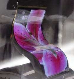
The film stack building up an OLED on a flexible substrate such as flexibel glass, plastic or a metal foil (schematic above from OLED-Display.net).
 
According to Erich Strasser at OLED-Display.net there are the development and market entry stages:
  • very thin > 0.25mm, light, unbreakable
  • Bendable, ready for production (Galaxy Round, LG-Flex)
  • Rollable, completely flexible –> ready 2016
  • Printable, displays like a paper –> ready 2018-2020


MEMS and NEMS Processing Advances one day workshop presented by Oxford Instruments Plasma Technology and IEMN

MEMS and NEMS Processing Advances one day workshop presented by Oxford Instruments Plasma Technology and IEMN.
 
This workshop is open to all those people working in industry and academia, with an interest in recent progress in research and development, plus future trends in the fabrication and application of micro & nano structures and devices.


An interactive, one day technical seminar focused on practical applications, techniques and advances.

This technical workshop is being hosted in conjunction with the Institute of Electronics Micro-electronics and Nanotechnology (IEMN) in Lille. It is a one day event aimed at all those scientists working in research and manufacturing with an interest in MEMS and NEMS, and is designed to keep participants abreast of the latest technologies and trends in these hot industry research topics.

Talks will include topics such as:
  • MEMS – how to make the nanoworld smaller
  • Nanoscale etch
  • MEMS research applications and results - IEMN
  • Looking towards the next generation of MEMS devices – a leading research organisation
  • ALD for MEMS – Eindhoven University
  • ALD research and results – Guest speaker
More information can be found here.
 
The workshop is free of charge however advance booking is essential. Register your place here.

Beneq-Glaston TFC2000™ for continuous production of TCO-glass

The Beneq-Glaston TFC2000™ is an off-line system designed for continuous production of TCO-coated glass for the solar industry. It represents a unique and seamless combination of the world-leading glass and annealing know-how of Glaston and Beneq nAERO® thin film TCO-coating.
 
Cost efficiency
  • high deposition efficiency – higher coating growth rate than competing technology
  • precursor yield 20% or better – save on materials
  • fast and easy entry to TCO solar glass
High quality
  • durable pyrolytic hard coating – high resistance against wear and tear
  • adjustable level of haze – enables TCO-coatings for different types of solar cells


The TFC2000 is designed for continuous production of TCO-coated glass for the solar industry. It represents a unique and seamless combination of the world-leading glass and annealing know-how of Glaston and Beneq nAERO® thin film TCO-coating.

Nanoscale pillars could radically improve conversion of heat to electricity, say CU-Boulder researchers

February 20, 2014 • Natural Sciences, Engineering, Energy • Discovery & Innovation University of Colorado Boulder scientists have found a creative way to radically improve thermoelectric materials, a finding that could one day lead to the development of improved solar panels, more energy-efficient cooling equipment, and even the creation of new devices that could turn the vast amounts of heat wasted at power plants into more electricity. The technique—building an array of tiny pillars on top of a sheet of thermoelectric material—represents an entirely new way of attacking a century-old problem, said Mahmoud Hussein, an assistant professor of aerospace engineering sciences who pioneered the discovery. The thermoelectric effect, first discovered in the 1800s, refers to the ability to generate an electric current from a temperature difference between one side of a material and the other. Conversely, applying an electric voltage to a thermoelectric material can cause one side of the material to heat up while the other stays cool, or, alternatively, one side to cool down while the other stays hot. - See more at: http://www.colorado.edu/news/releases/2014/02/20/nanoscale-pillars-could-radically-improve-conversion-heat-electricity-say#sthash.QSAijsdJ.dpuf
 
In a paper published in the journal Physical Review Letters, Hussein and Bruce Davis demonstrate a Nanophonic Metamaterial: 
 
Phys. Rev. Lett. 112, 055505 – Published 7 February 2014
Bruce L. Davis and Mahmoud I. Hussein

Abstract

We present the concept of a locally resonant nanophononic metamaterial for thermoelectric energy conversion. Our configuration, which is based on a silicon thin film with a periodic array of pillars erected on one or two of the free surfaces, qualitatively alters the base thin-film phonon spectrum due to a hybridization mechanism between the pillar local resonances and the underlying atomic lattice dispersion. Using an experimentally fitted lattice-dynamics-based model, we conservatively predict the metamaterial thermal conductivity to be as low as 50% of the corresponding uniform thin-film value despite the fact that the pillars add more phonon modes to the spectrum.
 
Comparison of the phonon dispersion and thermal conductivity of a pillared silicon thin film with a corresponding uniform thin film. The dispersion curves are colored to represent the modal contribution to the cumulative thermal conductivity, normalized with respect to the highest modal contribution in either configuration. The full spectrum is shown in (a) and the 0≤ω≤2.5  THz portion is shown in (b). Phonon DOS and the thermal conductivity, in both differential and cumulative forms, are also shown. The gray regions represent the difference in quantity of interest between the two configurations. The introduction of the pillar in the unit cell causes striking changes to all these quantities. [from online abstract: Phys. Rev. Lett. 112, 055505 – Published 7 February 2014]
 

Altatech (Soitec) to install new ALD/CVD system at Helmholtz-Zentrum Berlin


"Soitec’s Altatech subsidiary partners with Helmholtz-Zentrum Berlin and installs new CVD system

Altatech Semiconductor S.A. of Montbonnot, near Grenoble, France (a subsidiary of Soitec since January 2012) and Helmholtz-Zentrum Berlin für Materialien und Energie (HZB, a member of the Helmholtz Association of German Research Centres) have launched a collaborative partnership for R&D on materials for next-generation high-efficiency solar cells, including new classes of materials and innovative device structures for photovoltaic and photocatalysis applications.


The AltaCVD system will be used at EMIL to deposit amorphous silicon (alloys), transparent conductive oxides and ultra-thin dielectrics used in fabricating next-generation solar energy devices. The new EMIL building is adjacent to the third-generation storage ring BESSY II, and the cluster tool will be directly connected to an X-ray analytical end-station that accesses a dedicated beam line from BESSY II. Altatech and HZB will conduct atomic-layer deposition (ALD), plasma-enhanced chemical vapor deposition (PECVD) and physical vapor deposition (PVD) on substrates ranging from small research samples up to fully industry-compatible 6-inch wafers and use EMIL’s analytical capabilities to analyze material and interface properties in between successive processing steps. "
 
Further details in this press release:
 http://www.semiconductor-today.com/news_items/2014/FEB/ALTATECH_200214.shtml

Press release  from Helmholtz-Zentrum Berlin:
 http://www.helmholtz-berlin.de/pubbin/news_seite?nid=13925&sprache=en&typoid=49880

A cluster tool for the research on new classes of materials and device structures for photovoltaic and photocatalysis applications. (Source: Altatech)


Friday, February 21, 2014

HfO2 still going strong for Post-Silicon Channel Materials

According to a recent article HfO2 still going strong for Post-Silicon Channel Materials!
 
"Once device-grade channel materials are achieved, formation of a high quality gate dielectric is the next step. Here, recent results offer reason for optimism. As previously discussed, an initial Al2O3 deposition does not appear to be needed to passivate the InGaAs interface. While a clean surface is essential for successful gate oxide deposition, and atomic layer deposition appears to be an enabling technology for surface preparation, D. Hassan Zadeh and coworkers also obtained good results with La2O3 dielectrics. This material, along with HfO2, offers much a higher dielectric constant than Al2O3, improving ultimate scalability of alternative channel devices."
 
 
Read all about it on "New Challenges For Post-Silicon Channel Materials", by Katherine Derbyshire, Semiconductor Engineering: http://semiengineering.com/next-steps-for-post-silicon-channel-materials/

As reported by CompoundSemiconductor, Engineers from MIT are claiming to have fabricated the first tunnel FET with a double quantum well InGaAs/GaAsSb structure. This work has been published in: IEEE Electron Dev. Lett. 34 1503 (2013). MIT demonstrate employing HfO2 high-k on an InGaAs channel.


Engineers from MIT have fabricated a double quantum well FET (a). Cross-sectional tunnelling electron microscopy provides images of the tunnelling junction and gate stack in the gated region (b), and the edge of the InGaAs air bridge (c). A top view of the air-bridge, after suspension, is provided by a scanning tunnelling microscope (d) [as reported by CompondSemiconductor.net].

The Virtual Project on the History of ALD (VPHA) are looking for more contributors

"In the Virtual Project on the History of ALD (VPHA), we are still looking for more contributors (now we are with 35). Expertise of ALD on carbon or on porous materials would be especially useful. Also people are needed who know Russian language, and also some German speakers. Despite these "special requests", everyone, who knows a bit about ALD and speaks "only" English can contribute meaningfully. In return for volunteering, a position is offered as an author of the ALD history presentations to come, at Baltic ALD in May in Helsinki and at the AVS-ALD meeting in June in Kyoto."
 
Riikka Puurunen (Dr.), Senior Scientist, VTT Technical Research Centre of Finland
Jonas Sundqvist (Dr.), Group Leader High-k Devices, Fraunhofer IPMS-CNT, Germany
Annina Titoff, editor-in-chief, www.aldpulse.com
 
BALD 2014, Helsinki : http://www.aldcoe.fi/bald2014/
AVS-ALD 2014, Kyoto : http://www.ald2014.org/             

Thursday, February 20, 2014

Veeco ship first Prototype System for FAST-ALD™ for OLED to Samsung

According to the 4Q/2013 results press release  Veeco book first Prototype System for FAST-ALD™
 
"while not included in reported fourth quarter bookings, we received a purchase order from the world leader in mobile OLED displays for a next generation Fast Array Scanning Atomic Layer Deposition (FAST-ALD™) prototype system."


Recent information has become availabel that the system is heading to Samsung "Veeco sold a FAST-ALD flexible OLED encapsulation prototype system to Samsung". Who else could it bee since Samsung has 95% of that market? It is also in lign with previous reports on Synos Technology working with Samsung for Flexible OLED encapsulation.


Check out the cool animated video below to understan more about FAST-ALD a.k.a. Spatial ALD. Further reading on this technology you can find on the Veeco page for FAST-ALD : http://www.veeco.com/promos/fast-ald.aspx, where the key benefits are listed as:
 
  • Ultra-fast ALD process with continuous substrate scan Large substrate scalability without losing process throughput
  • Excellent uniformity with closed loop linear reactor design
  • Low CoO with high efficient gas-solid reaction process
  • Simultaneous In-line multi-process capability
 

Other companies that are developing or producing Spatial ALD Equipmet:

Wednesday, February 19, 2014

6th Leti Workshop on Innovative Memory Technologies


For the 6th time, Leti is hosting a workshop on innovative memory technologies at MINATEC on Tuesday, June 24, 2014, Grenoble, France. The workshop will explore the latest achievements in semiconductor memory technologies. Topics will range from short-term to long-term memory solutions, including:
 
·        Flash memories for embedded or stand-alone applications.
·        Resistive memory technologies such as phase-change memories, conductive bridging memories, oxide–based memories and magnetic memories.
·        Innovative ideas covering non-volatile logics and bio-inspired architectures.


The workshop will feature presentations given by both industrial and academic researchers. Invited contributions will be presented by leaders in the global memory industry.

To know more about previous editions of the workshop, please visit:

2012 edition:
http://leti.congres-scientifique.com/workshopmemories2012/index.php?onglet=5


2013 edition:
http://www.leti-innovationdays.com/index.php?langue=en&onglet=10


Tuesday, February 18, 2014

Samsung 3D-VNAND Promo Video and scaling in 3D

Samsung has been mass-producing 3D NAND modules since August last year according to this source. Here is a most informative news on Samsung 3D-VNAND technology from iTers News discussing limits to 2D scaling beyond 10 nm and "3D scaling".


Here is a interesting presentation from Applied Materials on 3D NAND "Winning in 3D NAND" explaining quite some details on process requirements for going from 2D to 3D technology.
 

"Advantage of 3D NAND is that it doesn’t require leading-edge lithography…the burden will shift from lithography to deposition and etch."  Ritu Shrivastava, VP Technology, SanDisk, May 2013 (SemiMD) [Picture is a screenshot from Applied Materials presentation linked above]

ALD4PV Workshop at Eindhoven University of Technology (Eindhoven, The Netherlands) - March 20th, 2014

The workshop will highlight the relevance and potential of ALD for crystalline silicon solar cells, copper indium gallium selenide (CIGS) solar cells, dye-sensitized solar cells (DSC) and other emerging solar cell concepts. Furthermore, the upscaling of the ALD technology for the PV industry will be discussed.


 The program includes invited presentations by Dr. Alex Martinson (Argonne National Laboratory, US), Dr. Tobias Törndahl (Uppsala University, SE), Dr. Joachim John (IMEC, BE) and Dr. Ernst Granneman (Levitech, NL) as well as several contributed presentations.

More details on the workshop, program and registration can be found at :

ALD - Quantum discovery, analysis, and optimization of reactive precursors. Webinar February 20th, 2014

 
Dr. Mathew D. Halls, Director of Materials Science, will present "Quantum discovery, analysis, and optimization of reactive precursors for thin-film deposition with the Materials Science Suite" on Thursday, February 20. Dr. Halls will provide an overview of the Materials Science Suite applied to reactive precursors and demonstrate the use of high-throughput quantum chemistry to more reliably identify candidate organometallic precursors based on chemical reaction energetics for model surface reaction pathways.
 
 
Quantum discovery, analysis, and optimization of reactive precursors for thin-film deposition with the Materials Science Suite
Dr. Mathew D. Halls
Senior Director, Materials Science
First-principles simulation has become a reliable tool for the prediction of structures, chemical mechanisms, and reaction energetics for the fundamental steps in processes such as Atom Layer Deposition (ALD). In addition to reaction energies and structural information, quantum-based simulation can also be used to compute vibrational spectra, enabling the conclusive assignment of gas-phase precursor and surface adsorbate-related bands. Such predictive capability raises the possibility for computational discovery and design of new reactive precursors with enhanced properties. Computational structure enumeration of precursor libraries and the automated quantum mechanical analysis of reaction energies opens a new mode of computational discovery for reactive systems.

In this presentation, Dr. Halls provides an overview of the Schrödinger Materials Science Suite applied to reactive precursors and demonstrates the use of high-throughput quantum chemistry to more reliably identify candidate organometallic precursors based on chemical reaction energetics for model surface reaction pathways.
 
 
Webinar February 20th, 2014 15:00 CET
Registration: Here
 

Monday, February 17, 2014

HZDR in Germany is printing sub-50 nm nearly-discrete magnetic patterns using chemical disorder induced ferromagnetism

HZDR in Germany is printing nearly-discrete magnetic patterns using chemical disorder induced ferromagnetism. Materials in which the magnetic behavior can be tuned via ion-induced phase transitions may allow the fabrication of novel spin-transport and memory devices using existing lateral patterning tools.


Original publication:
 
Printing Nearly-Discrete Magnetic Patterns Using Chemical Disorder Induced Ferromagnetism
Rantej Bali et al
Nano Lett., 2014, 14 (2), pp 435–441
 
 
Abstract:
 
Ferromagnetism in certain alloys consisting of magnetic and nonmagnetic species can be activated by the presence of chemical disorder. This phenomenon is linked to an increase in the number of nearest-neighbor magnetic atoms and local variations in the electronic band structure due to the existence of disorder sites. An approach to induce disorder is through exposure of the chemically ordered alloy to energetic ions; collision cascades formed by the ions knock atoms from their ordered sites and the concomitant vacancies are filled randomly via thermal diffusion of atoms at room temperature. The ordered structure thereby undergoes a transition into a metastable solid solution. Here we demonstrate the patterning of highly resolved magnetic structures by taking advantage of the large increase in the saturation magnetization of Fe60Al40 alloy triggered by subtle atomic displacements. The sigmoidal characteristic and sensitive dependence of the induced magnetization on the atomic displacements manifests a sub-50 nm patterning resolution. Patterning of magnetic regions in the form of stripes separated by 40 nm wide spacers was performed, wherein the magnet/spacer/magnet structure exhibits reprogrammable parallel (↑/spacer/↑) and antiparallel (↑/spacer/↓) magnetization configurations in zero field. Materials in which the magnetic behavior can be tuned via ion-induced phase transitions may allow the fabrication of novel spin-transport and memory devices using existing lateral patterning tools.
 
[Based on original German News, Ionenstrahlen ebnen den Weg zu neuen Ventilen für die Spintronik and Rossendorfer arbeiten an Ventilen für Spintronik-Chips]

Video from the manufacturing line at Plastic Logic's Dresden facility

Recently a video was released from Plastic Logic from the manufacturing factory in Dresden - If you´re in to Fab Automation you will like this one!
 
Plastic Logic is a spin-off company from Cambridge University's Cavendish Laboratory and specialises in polymer transistors and plastic electronics. The company was founded in 2000 by Professor Sir Richard Friend, Professor Henning Sirringhaus and Stuart Evans. The company develops and manufactures color and monochrome plastic flexible displays in various sizes based on an organic thin film transistor (OTFT) technology. The headquarters of Plastic Logic is in Cambridge, United Kingdom. [Wikipedia, 2014-02-17]
 
Plastic Logic runs a commercial, high-volume organic electronics factory manufacturing plastic displays in Dresden, Germany. Check out the Video below!

Saturday, February 15, 2014

Using Oxford Instriments OpAl TiN ALD to create high strength low weight Nano Meta Materials

Fabrication and deformation of three-dimensional hollow ceramic nanostructures
Dongchan Jang, Lucas R. Meza, Frank Greer, Julia R. GreerNature Materials, 12 (2013) 893–898, DOI:doi:10.1038/nmat3738
 
 
Image Thumbnail


Above: Skeletal natural biological materials versus TiN nanolattices.

In the analysis of complex, hierarchical structural meta-materials, it is critical to understand the mechanical behavior at each level of hierarchy in order to understand the bulk material response. We report the fabrication and mechanical deformation of hierarchical hollow tube lattice structures with features ranging from 10 nm to 100 μm, hereby referred to as nanolattices. Titanium nitride (TiN) nanolattices were fabricated using a combination of two-photon lithography, direct laser writing, and atomic layer deposition. The structure was composed of a series of tessellated regular octahedra attached at their vertices. In situ uniaxial compression experiments performed in combination with finite element analysis on individual unit cells revealed that the TiN was able to withstand tensile stresses of 1.75 GPa under monotonic loading and of up to 1.7 GPa under cyclic loading without failure. During the compression of the unit cell, the beams bifurcated via lateral-torsional buckling, which gave rise to a hyperelastic behavior in the load–displacement data. During the compression of the full nanolattice, the structure collapsed catastrophically at a high strength and modulus that agreed well with classical cellular solid scaling laws given the low relative density of 1.36 %. We discuss the compressive behavior and mechanical analysis of the unit cell of these hollow TiN nanolattices in the context of finite element analysis in combination with classical buckling laws, and the behavior of the full structure in the context of classical scaling laws of cellular solids coupled with enhanced nanoscale material properties.

 
Screendump from the video below, showing the fabrication method of the 3D architected nano meta materials described in the Nature publication above.


Video from Solve for X - Julia Greer - 3D Architechted Nano Metamaterials at World Economic Forum.


According to the information I have the ALD TiN process was performed in an OpAL Atomic Layer Deposition System from Oxford Instruments

The Julia Greer Group at Caltech: http://www.jrgreer.caltech.edu/home.php

Idea and inspiration for this post taken from the Next Big Future Blog.

Tuesday, February 11, 2014

Pacemaker powered by piezoelectric energy harvesting technology


University of Arizona reports on "Tiny power generators developed by the University of Arizona and the University of Illinois could eliminate the need for batteries in medical devices.

The miniature devices consist of piezoelectric nanoribbons sandwiched between two thin layers that serve as electrodes, one made of titanium and platinum and the other made of chromium and gold. Piezoelectric elements are crystals that generate an electrical current when deformed under mechanical pressure and are used in many applications, such as disposable lighters and mini speakers."


The mechanical energy harvester, which is flexible enough to conform to the surface of an organ such as the heart, converts the organ's motion into electricity. (Photo: Univ. of Illinois/UA)An energy harverster for an implanted medical device could still though need an energy storage, e.g., for comunicating with the outside world thru wireless communication were more power is need under short period of time.

Check out our extremely thin (2 to 10 µm) on chip 3D capacitor technology at Fraunhofer CNT that has exactly this type application in mind!

 
SEM a) cross section of a trench array with AR 13:1 filled with MIM stack and b) top down micrograph of Si trench array after silicon etch. Current technology is 1:20 and gives 220nF/mm2 with a goal for 1000nF/mm2 in the near future.

Sunday, February 9, 2014

ARM is evaluating CeRAM technology for embedded NVM

ARM is evaluating CeRAM - correlated electron random access memory - technology for embedded NVM according to a recent statment from Symetrix:

"ARM is evaluating CeRAM technology as part of its strategy in embedded nonvolatile memory offerings and their discussions with Symetrix started over three months ago. Symetrix will provide its technology and the results from Symetrix programs ongoing at the University of Texas (Dallas) and the University of Colorado (Colorado Springs) to chip foundries engaged by ARM. Other chip companies are also working with Symetrix under similar terms."


EE Times also reported on this and CeRAM technology here: CeRAM Memory Gets ARM's Attention:

"CeRAM is based on a transition metal oxide, in this case nickel oxide (NiO). The premise is that, by cleaning up NiO through a suitable doping technique, it is possible to obtain electrically conducting NiO that can make very rapid, reversible, nonvolatile bulk transitions between its electrically insulating and conducting states. In the past, these transitions were possible only at a high pressure and temperature, but they now can be achieved at room temperature with low switching voltages and currents. Key to the operation is a reversible metal-to-insulator transition (MIT) that has its roots in the work of Sir Nevill Mott and John Hubbard. "

Here is a descriptive presentation from Symetrix that goes into detail on CeRAM and compares it to the more mainbstream ReRAM technology. In short:

1) CeRAM vs. Filament Technologies (ReRAM) according to Symetrix
• Control of material properties and proper device architecture are fundamental to this new paradigm. Evidence? No filament formation. (No electroforming)
• The CeRAM resistor is designed to exploit materials properties, surface properties, switching mechanism (endurance) and memory mechanism (retention).
• Optimizing CeRAM is a different science than building the perfect filament.


Unlike ReRAM, CeRAM is resistive memory which uses the same transition metal oxide (TMO), such as NiO, but strands are not used and electroplating. Instead CeRAM-memory quantum correlation effects observed positions of electrons, where it got its name. In the structure of the active region is allocated CeRAM TMO, which separates the two conductive layers TMO, whereas in the transition metal oxide ReRAM occupies entire domain between the metal layers.
2) CeRAM STATUS according to Symetrix:
THEORY: Confirmed with empirical results DONE
MATERIALS: Doping any TMO with any extrinsic ligand PATENTED
PROCESS: Create and isolate thin (5 nm) active region by simple spin-on or ALD PATENT FILED
ARCHITECTURE: Array only (no pass gate) PATENTED
3-D (STACKING) With only silicon friendly materials IN PROCESS
FPGA Architecture PATENT FILED

Further References on CeRAM:

Patents:
16 Patents by Symetrix (as assignee) on "correlated electron memory" as returned from Google Patent search.

Publications on CeRAM:

“A non-filamentary model for unipolar switching transition metal oxide resistance random access memories”, Kan-Hao Xue, Carlos Paz De Araujo, Jolanta Celinska, and Christopher McWilliams, J. Appl. Phys. 109, 091602 (2011)

“Material and process optimization of correlated electron random access memories”, Jolanta Celinska, Christopher McWilliams, Carlos Paz De Araujo, and Kan-Hao Xue, J. Appl. Phys. 109, 091603 (2011)

“Device characterization of correlated electron random access memories”, Christopher McWilliams, Jolanta Celinska, Carlos Araujo, and Kan-Hao Xue, J. Appl. Phys. 109, 091608 (2011)

“Operating Current Reduction in Nickel Oxide Correlated Electron Random Access Memories (CeRAMs) through Controlled fabrication Processes”, Jolanta Celinska, Christopher McWilliams, Carlos Paz De Araujo, and Kan-Hao Xue, Integrated Ferroelectrics, 124, 105-111 (2011)

“Re-Programmable Antifuse FPGA Utilizing Resistive CERAM Elements”, Christopher McWilliams, Carlos Paz De Araujo, Jolanta Celinska, and Kan-Hao Xue, Integrated Ferroelectrics, 124, 97-104 (2011)

Thursday, February 6, 2014

PVD Free processes used for future emerging memory technologies

This week at the Fraunhofer IPMS-CNT Industry Day, Malgorzata Jurczak, Director Emerging Memory Devices - IMEC, stated that "PVD-free processes (ALD/CVD) are needed for Emerging Memory" To visualize this in the case of 3D NAND there is a recent blog post (SemiMD.com) on the topic - and yes obviously PVD and also not CVD can´t be an option for these highly scaled 3D architectures. Below is a brief snapshot [complete story here]

"The current iteration of NAND flash technology, 2D – or planar – NAND, is reaching its limits. In August 2013, South Korean consumer electronics brand Samsung announced the launch of its 3D NAND storage technology, in the form of a 24-layer, 128 GB chip. In 2014, memory chipmakers Micron and also SK Hynix will follow suit, heralding the arrival of a much-anticipated and debated technology during various industry conferences in recent years. Other companies, including Sandisk, are all working on 3D NAND flash technology." as reported by
Sara Ver-Bruggen, contributing editor at Semiconductor Manufacturing and Design.

“Everything in 3D is a significant challenge. With vertical scaling the challenges include etching high aspect ratio holes, with the aspect ratio doubling with each doubling of layers. These holes must have absolutely parallel walls or scaling and device operation may be compromised. If the layers are thinned then the atomic-layer deposition (ALD) of the layers must be able to apply a constant thickness layer across the entire wafer, which is also true of the layers that are deposited on the walls of the hole,” according to Handy. [Jim Handy from Objective Analysis, who is writing aboute NAND and 3D NAND in the Memory Guy Blog]

 
3D NAND manufacturing considerations and challenges - Staircase etching requires very precise contact landing and the ALD process has to be applied with a constant thickness in 3D across the whole 300mm wafer. Obviously PVD or CVD is not an option at all. These staircase contacts could have an 60:1 aspect ratio.
Chuck Dennison, Senior Director Process Integration, from Micron, explained for 3DNAND “There is a lot planarization, you are etching very high aspect ratio contacts where you need to be very controlled, in terms of how you define your control and CD uniformity. Then there are a lot of additional modules requiring ALD deposition. So we think that there is a lot of opportunity to utilize our DRAM expertise.”

Wednesday, February 5, 2014

KIT demonstrates lightweight ALD coated material that mimics the structure of bone


"High-strength cellular ceramic composites with 3D microarchitecture" Bauer et al., Karlsruhe Nano Micro Facility, Karlsruhe Institute of Technology, D-76131 Karlsruhe, Germany LINK (10.1073/pnas.1315147111, including supporting free avaialble material, videos and pictures)
 
Uniaxial compression test of a polymeric truss structure (right). Failure due to local buckling of diagonal struts under compressive load is followed by large plastic deformations and fracture. Before the collapse, bending of single struts due to processing-related predeformation (shrinking effects) also is observed. Uniaxial compression test of a polymeric truss structure (left) coated with 10 nm of [ALD] Al2O3. Local buckling of individual vertical compression bars leads to the immediate collapse of the whole structure. Only a little plastic deformation can be observed.

Abstract:
To enhance the strength-to-weight ratio of a material, one may try to either improve the strength or lower the density, or both. The lightest solid materials have a density in the range of 1,000 kg/m3; only cellular materials, such as technical foams, can reach considerably lower values. However, compared with corresponding bulk materials, their specific strength generally is significantly lower. Cellular topologies may be divided into bending- and stretching-dominated ones. Technical foams are structured randomly and behave in a bending-dominated way, which is less weight efficient, with respect to strength, than stretching-dominated behavior, such as in regular braced frameworks. Cancellous bone and other natural cellular solids have an optimized architecture. Their basic material is structured hierarchically and consists of nanometer-size elements, providing a benefit from size effects in the material strength. Designing cellular materials with a specific microarchitecture would allow one to exploit the structural advantages of stretching-dominated constructions as well as size-dependent strengthening effects. In this paper, we demonstrate that such materials may be fabricated. Applying 3D laser lithography, we produced and characterized micro-truss and -shell structures made from alumina–polymer composite. Size-dependent strengthening of alumina shells has been observed, particularly when applied with a characteristic thickness below 100 nm. The presented artificial cellular materials reach compressive strengths up to 280 MPa with densities well below 1,000 kg/m3.
 

Monday, February 3, 2014

There´s hope for a Good Hair Day for a BALD Engineer!

Good hair day: New technique grows tiny 'hairy' materials at the microscale

"(Nanowerk News) Scientists at the U.S. Department of Energy's Argonne National Laboratory attacked a tangled problem by developing a new technique to grow tiny “hairy” materials that assemble themselves at the microscale"

Actually there is more than hope, there is a also a hair vax to go with the micro hair - and yes it is made by ALD!

"In one experiment the researchers used a process called atomic layer deposition that deposits a molecule-thick layer of material over the entire hairy structure, like a fresh blanket of snow, to add a layer of semiconductor material. Semiconductors are essential ingredients in many technologies, such as solar cells and electronics"


Argonne materials scientists announced a new technique to grow these little forests at the microscale (the scale shows 100 micrometers, which is about the diameter of a single human hair). (Image by Alexey Snezhko and Igor Aronson)

Read more: Good hair day: New technique grows tiny 'hairy' materials at the microscale
For all Moomin fans the resembelence with the electrified Hatifnats is stunning :-)


Sunday, February 2, 2014

SENTECH Plasma Process Technology Seminar 2014 Feb. 27th

Sentech (www.sentech.de) announces that "In good tradition SENTECH is glad to announce its annual Plasma Seminar which takes place on Thursday, February 27th, 2014 at SENTECH Instruments GmbH, Schwarzschildstraße 2, Berlin Adlershof.

 
As the global interest in Nanotechnology is growing, we want to get our participants introduced to new topics in fields of deposition and etching combined with recent examples. Invited speakers will focus on topics such as the deposition through ALD and PE-ALD, the etching of micro- and nanostructures in Si, the manufacturing of graphene films and the deposition of passivation and encapsulation films through IC PECVD and ALD. The whole Seminar Program can be downloaded here: Programme_SENTECH Plasma Seminar . If you want to participate please send this Registration for SENTECH`s Plasma Process Technology Seminar to: sales@sentech.de
 
After the seminar there will be a presentation of the SENTECH application laboratories and its production facilities. The whole material of this seminar will be provided for all participants.
For further information don`t hesitate to contact us or call: +49 89 8979607-0"

IBIS predict that cost/gate is now increasing and thus is no longer an economic driver to move to the next node


At a Semi Industry Strategy Symp (ISS) Int Business Strategies (IBS) presented a forecast for the semiconductor industry until 2020. i-Micronews reports on this event here.

"IBIS predict that cost/gate is now increasing and thus is no longer an economic driver (for same wafer size) to move to the next node."


Interesting graph that shows that 28nm is the cheapest node ever (per gate) and will probably stay so unless 450mm wafers will make a difference. As we all know 450mm has been delayed again, meaning 28nm will probably be the dominating node for a long time to come.

The IBIS report concludes:

"IBIS further predicts that:
- 28nm will have long lifetime ( Probability 80% )
- 20nm yields will improve, and will be high volume technology node in 2015 and 2016 (Probability 50%)
- 16/14nm will provide low cost gates and support high bandwidth interfaces in SoC environment (Probability 20% in 2016 and 50% in 2017)
- 10nm will likely be postponed, cost per gate will be prohibitive and unclear as to demand other than high speed processors and FPGAs (Probability 90%)."

According to IC Insights’ ranking of the leading IC foundries, "... the top 13 foundries in the figure represented 91% of total foundry sales in 2013. For comparison, the leading 13 foundries accounted for 84% of total foundry marketshare in 2009, the year before Samsung dramatically ramped up its IC foundry production for Apple."


Saturday, February 1, 2014

BENEQ nSILVER coating for special edition coins in honor of Tove Jansson - creator of The Moomins

ALDpulse.com reports that Mint of Finland will mint a special issue of 100 numbered Tove Jansson coins with a nominal value of EUR 20. The special edition coins will be given anti-tarnish nSILVER ALD coating developed by the Finnish company Beneq (www.beneq.com).
 
 
The Tove Jansson collector coin will be issued on 7 February. It will be available on the Mint of Finland online shop and from distributors.
Jansson is best known as the author of the Moomin books for children. The first such book, The Moomins and the Great Flood, appeared in 1945, though it was the next two books, Comet in Moominland and Finn Family Moomintroll, published in 1946 and 1948 respectively, that brought her fame. Tove Jansson was selected one time previously as the main motif in the 2004 minting of a Finnish commemorative coin, the €10 Tove Jansson and Finnish Children's Culture commemorative coin. [Wikipedia]


ALD:ed Tove Jansson €20 coin from Mint of Finland. The coins have been coated with nSILVER(R) from BENEQ to protect them from oxidation.

More information on the BENEQ nSILVER coating you can find here and below you can watch a Video on development of silver saving technology by University of Maryland using a BENEQ TSF 500 Batch ALD reactor.