


%20(1).png)
Vanderbilt University reported - How to create nanowires only three atoms wide with an electron beam -
"Junhao Lin, a Vanderbilt University Ph.D. student and visiting scientist at Oak Ridge National Laboratory (ORNL), has found a way to use a finely focused beam of electrons to create some of the smallest wires ever made. The flexible metallic wires are only three atoms wide: One thousandth the width of the microscopic wires used to connect the transistors in today’s integrated circuits."
“This will likely stimulate a huge research interest in monolayer circuit design,” Lin said. “Because this technique uses electron irradiation, it can in principle be applicable to any kind of electron-based instrument, such as electron-beam lithography.”
One of the intriguing properties of monolayer circuitry is its toughness and flexibility. It is too early to predict what kinds of applications it will produce, but “If you let your imagination go, you can envision tablets and television displays that are as thin as a sheet of paper that you can roll up and stuff in your pocket or purse,” Pantelides commented.
In addition, Lin envisions that the new technique could make it possible to create three-dimensional circuits by stacking monolayers “like Lego blocks” and using electron beams to fabricate the wires that connect the stacked layers.
Full report from Vanderbilt University can be found here and please check out the video and the publication below for more insights!
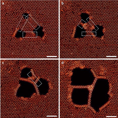
Series of still scanning electron micrographs (a to d) show how the electron beam is used to create nanowires. (Junhao Lin / Vanderbilt)
Junhao Lin, a Vanderbilt University Ph.D. student and visiting scientist at Oak Ridge National Laboratory (ORNL), has found a way to use a finely focused beam of electrons to create flexible metallic wires that are only three atoms wide: One thousandth the width of the microscopic wires used to connect the transistors in today's integrated circuits and some of the smallest wires ever made. The discovery gives a boost to efforts aimed at creating electrical circuits on monolayered materials, raising the possibility of flexible, paper-thin tablets and television displays. [youtube.com]
Atomic mechanism of the semiconducting-to-metallic phase transition in single-layered MoS2
Yung-Chang Lin, Dumitru O. Dumcenco, Ying-Sheng Huang & Kazu Suenaga
Nature Nanotechnology (2014) doi:10.1038/nnano.2014.64 Published online 20 April 2014
Abstract:
Phase transitions can be used to alter the properties of a material without adding any additional atoms and are therefore of significant technological value. In a solid, phase transitions involve collective atomic displacements, but such atomic processes have so far only been investigated using macroscopic approaches. Here, we show that in situ scanning transmission electron microscopy can be used to follow the structural transformation between semiconducting (2H) and metallic (1T) phases in single-layered MoS2, with atomic resolution. The 2H/1T phase transition involves gliding atomic planes of sulphur and/or molybdenum and requires an intermediate phase (α-phase) as a precursor. The migration of two kinds of boundaries (β- and γ-boundaries) is also found to be responsible for the growth of the second phase. Furthermore, we show that areas of the 1T phase can be controllably grown in a layer of the 2H phase using an electron beam.
No comments:
Post a Comment