


%20(1).png)
According to a recent article HfO2 still going strong for Post-Silicon Channel Materials!
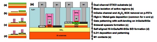
"Once device-grade channel materials are achieved, formation of a high quality gate dielectric is the next step. Here, recent results offer reason for optimism. As previously discussed, an initial Al2O3 deposition does not appear to be needed to passivate the InGaAs interface. While a clean surface is essential for successful gate oxide deposition, and atomic layer deposition appears to be an enabling technology for surface preparation, D. Hassan Zadeh and coworkers also obtained good results with La2O3 dielectrics. This material, along with HfO2, offers much a higher dielectric constant than Al2O3, improving ultimate scalability of alternative channel devices."
Read all about it on "New Challenges For Post-Silicon Channel Materials", by Katherine Derbyshire, Semiconductor Engineering: http://semiengineering.com/next-steps-for-post-silicon-channel-materials/
As reported by CompoundSemiconductor, Engineers from MIT are claiming to have fabricated the first tunnel FET with a double quantum well InGaAs/GaAsSb structure. This work has been published in: IEEE Electron Dev. Lett. 34 1503 (2013). MIT demonstrate employing HfO2 high-k on an InGaAs channel.

As reported by CompoundSemiconductor, Engineers from MIT are claiming to have fabricated the first tunnel FET with a double quantum well InGaAs/GaAsSb structure. This work has been published in: IEEE Electron Dev. Lett. 34 1503 (2013). MIT demonstrate employing HfO2 high-k on an InGaAs channel.

Engineers from MIT have fabricated a double quantum well FET (a). Cross-sectional tunnelling electron microscopy provides images of the tunnelling junction and gate stack in the gated region (b), and the edge of the InGaAs air bridge (c). A top view of the air-bridge, after suspension, is provided by a scanning tunnelling microscope (d) [as reported by CompondSemiconductor.net].
No comments:
Post a Comment